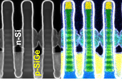
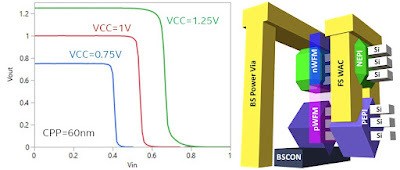
Intel researchers developed a 3D monolithic CFET device* with 3 n-FET nanoribbons atop 3 p-FET nanoribbons, separated by 30 nm gap. This industry-first device enabled the creation of functional inverters at a 60 nm gate pitch. Notably, it incorporated vertically stacked dual-Source/Drain epitaxy, dual metal work function gate stacks, and backside power delivery with direct device contacts. They also introduced a nanoribbon "depopulation" method for varying n-MOS/p-MOS device numbers. This research advances the understanding of CFET scalability for logic and SRAM applications and highlights key process enablers. The paper will be presented at the upcoming IEDM conference in San Francisco.
Comment: The stacked CMOS inverter at a 60 nm gate pitch represents an advancement in semiconductor design, allowing for denser circuits. The 60 nm distance between gates indicates a highly miniaturized design. Power vias provide vertical power connections to different layers, while direct backside device contacts enhance efficiency and heat dissipation. This development offers a glimpse into the future electronic devices being more compact, efficient, and high-performing than deploying "planar" designs in one layer like the FinFETs and GAA-FETs of today.
ALD plays a key role in manufacturing 3D monolithic CFET devices by assisting in crafting the architecture and providing atomically precise and even thin film layers at small scales. ALD ensures even coverage, which is important for 3D designs, especially on vertical areas and inside deep gaps. It's used to put down important materials in transistor gate stacks (High-k/Metal Gates or HKMG), as well as barrier and seed layers. ALD also helps in doping (SSD - solid state doping), which changes how semiconductors behave, and in creating spacers, important for separating and defining parts of transistors. In brief, ALD helps improve the CFET design and its overall performance.
* A 3D monolithic CFET device combines three-dimensional stacking and the Complementary Field-Effect Transistor (CFET) design within a single semiconductor structure. This approach vertically integrates both n-type and p-type transistors on the same substrate, promoting tighter integration and reduced interconnect delays. By leveraging the complementary operation of CFET and the benefits of 3D stacking, the device aims to enhance performance, miniaturization, and efficiency in semiconductor technology.


%20(1).png)


No comments:
Post a Comment