


%20(1).png)
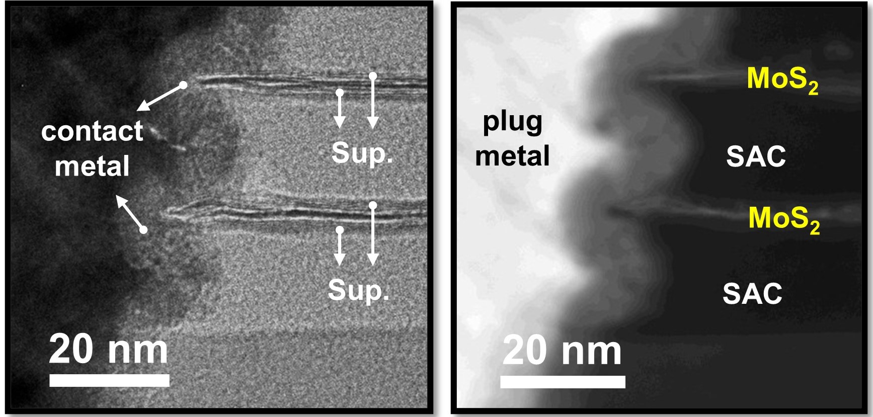
A TSMC-led research team, in collaboration with National Yang Ming Chiao Tung University and National Applied Research Laboratories, has unveiled promising results for using ultra-thin transition metal dichalcogenides (TMDs), specifically MoS2, as the channel material in NMOS nanosheets. Their innovative approach deviates from the conventional method of thinning Si channels. The team's devices exhibited impressive performance metrics: a positive threshold voltage (VTH) of ~1.0 V, a high on-current of ~370 µA/µm at VDS = 1 V, a large on/off ratio of 1E8, and a low contact resistance ranging between 0.37-0.58 kΩ-µm. These outcomes were primarily attributed to the introduction of a novel C-shaped wrap-around contact, which enhances contact area, and an optimized gate stack. While the devices demonstrated satisfactory mechanical stability, a challenge remains in addressing defect creation within the MoS2 channels. This groundbreaking study, titled "Monolayer-MoS2 Stacked Nanosheet Channel with C-type Metal Contact" by Y-Y Chung et al., is a pivotal step forward in nanosheet scaling using TMDs.
ALD is a the technique for the precise and uniform synthesis of MoS₂, especially for semiconductor applications on large-scale wafers. The choice of precursors plays a crucial role in achieving optimal deposition characteristics. Mo (CO) 6 and H2S have been identified as the primary precursors for depositing molybdenum and sulfur components, respectively. These precursors have demonstrated the capacity for self-limiting growth behavior within a specific ALD temperature window, leading to uniform MoS₂ layers. Notably, this process has been successfully scaled up to achieve highly uniform film growth on large 300 mm SiO2/Si wafers, marking its potential for industry-level manufacturing. The ability to maintain uniformity and thickness control on such wafers emphasizes the potential of ALD in integrating MoS₂ into next-generation electronic devices and further underscores the significance of selecting appropriate precursors for optimal deposition outcomes. Other precursors have been investigated. MoCl₅ and MoF₆ serve as alternative molybdenum sources. For the sulfur component, H₂S is commonly paired with molybdenum precursors, but (CH₃)₂S has also been explored. The choice of these precursors directly impacts the properties of the resulting MoS₂ film in the ALD process and therefore precursor development for 2D MoS2 is a hot field of ongoing research.
While deposition methods are abundant, etching processes are comparatively scarce. Recent research by Elton Graugnard et al also introduces a thermal Atomic Layer Etching (ALE) technique for MoS2, leveraging MoF6 for fluorination, alternated with H2O exposures, to etch both crystalline and amorphous MoS2 films. This process has been characterized using various analytical techniques like QCM, FTIR, and QMS. The etching is temperature-dependent, with a significant increase in mass change per cycle as temperature rises. The mechanism involves two-stage oxidation of Mo, producing volatile byproducts. The resultant etch rates were established for different films, and post-etch annealing rendered crystalline MoS2 films. The thermal MoS2 ALE introduces a promising low-temperature method for embedding MoS2 films in large-scale device manufacturing.

Chem. Mater. 2023, 35, 3, 927-936
Sources:
Best Ways To Recover Funds From Crypto and Bitcoin Scam - by Alpha Recovery Experts
ReplyDeleteAlthough recovering stolen cryptocurrency can be difficult, experts like Alpha Recovery Experts can assist you in getting your lost Bitcoin back. The team begins the cryptocurrency scam recovery process by looking into the story of events and the scheme’s timetable in order to guarantee a successful outcome for the recovery of lost assets. They then track down your virtual assets and examine the data that is at his disposal. Consult Alpha Recovery Experts if you wish to get your misplaced Bitcoin back.
Get in touch with them through,
E-mail (Alpharecoveryexpert@consultant.com)
Visit (Alpharecoveryexperts. com
Great post, well structured. It’s interesting how simple browser games can still offer engaging experiences. You can explore Geo dash. The game includes colorful stages, smooth mechanics, and clever obstacle patterns. Each level provides a different challenge, keeping the gameplay fresh while rewarding better timing and control.
ReplyDelete