Showing posts with label Graphene. Show all posts

Tuesday, December 3, 2024

Adisyn Acquires 2D Generation: Pioneering Low-Temperature Graphene for Next-Gen Semiconductors

Israeli-based 2D Generation (2DG), which specializes in graphene-based solutions for semiconductors, has been acquired by ASX-listed Adisyn (ASX:AI1), a provider of tech services for SMEs in the Australian defense sector that has expanded its focus to the semiconductor industry through this acquisition.

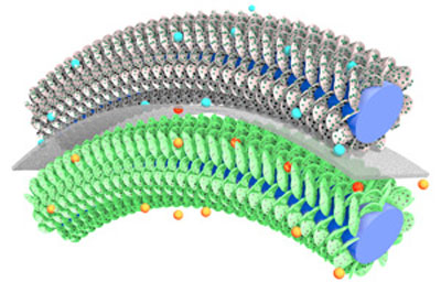
Israeli-based 2D Generation (2DG), a pioneer in graphene-based solutions for semiconductors, has been acquired by ASX-listed Adisyn (ASX:AI1), an Australian defense tech services provider now expanding into the semiconductor industry. Adisyn, a founder of the Connecting Chips European Union Joint Undertaking alongside NVIDIA, Valeo, and Applied Materials, gains access to 2DG’s patented low-temperature graphene production technology. Unlike traditional methods requiring temperatures of around 1,000°C—unsuitable for delicate semiconductor chips—2DG’s process uses Atomic Layer Deposition (ALD) to grow graphene below 300°C, ensuring compatibility with chip manufacturing. This breakthrough addresses a critical industry challenge: as transistors shrink, heat generation in interconnects limits performance and reliability. Graphene’s superior conductivity and heat resistance make it a transformative material for interconnects, potentially unlocking faster, more efficient chips. 2DG’s CEO Arye Kohavi emphasizes the technology's importance for overcoming bottlenecks in chip design, with discussions already underway with industry giants like TSMC and Nvidia. As 2DG scales its ALD capabilities, it aims to integrate graphene into next-generation chips, potentially revolutionizing applications from EVs to AI systems and positioning the company as a key player in the semiconductor sector.


Adisyn Ltd (ASX: AI1) has announced the acquisition of a state-of-the-art Atomic Layer Deposition (ALD) machine from Beneq, a leader in deposition technology, to advance its subsidiary 2D Generation Ltd’s innovative semiconductor solutions. The ALD system will enable precise, ultra-thin graphene layering on semiconductor interconnects, addressing critical bottlenecks in chip manufacturing and paving the way for transformative advancements in high-performance computing, including generative AI, data centers, and defense applications. Scheduled for installation within the next 5-6 months, this equipment represents a crucial step in scaling production of graphene-coated interconnects to enhance speed, energy efficiency, and scalability in semiconductor technology.


Recently, 2D Generation has also partnered with M&T Semiconductor, a leading specialty semiconductor advisory firm founded by industry veterans Dr. Itzhak Edrei and Zmira Shterenfeld Lavie, to accelerate the development and commercialization of its groundbreaking graphene technology. This collaboration aims to secure strategic partnerships with semiconductor fabricators, fabless chipmakers, and equipment vendors while prioritizing licensing opportunities and potential buyouts. M&T brings decades of expertise from Tower Semiconductor, leveraging deep industry connections to advance 2DG’s patented sub-300°C graphene coating process, which addresses critical challenges in interconnect performance and scalability. With this partnership, 2DG is positioned to reshape semiconductor manufacturing and drive next-generation chip innovation.

M&T Semiconductor, founded in 2019, is a specialized advisory firm offering strategic consulting, mergers and acquisitions (M&A) services, and research and development (R&D) expertise in the semiconductor industry. Led by industry veterans Dr. Itzhak Edrei, former President of Tower Semiconductor, and Zmira Shterenfeld Lavie, former General Manager at Tower Semiconductor, M&T leverages over three decades of experience to assist clients in refining objectives, scouting technologies, and implementing processes.Their services encompass strategic consulting, M&A facilitation, technology scouting, and implementation, aiming to deliver tangible outcomes and foster partnerships within the semiconductor sector.


Sources:

2DG secures semiconductor advisor to develop initiatives - Adisyn Ltd (ASX:AI1) - Listcorp.

2DG a part of Adisyn to build new graphene for chip mfg


Saturday, November 16, 2024

Adisyn Ltd Invests in ALD Technology from Beneq Graphene Device Manufacturing

Adisyn Ltd has taken a significant step toward advancing semiconductor technology with its recent investment in an Atomic Layer Deposition (ALD) machine from Beneq. On November 10, 2024, the company announced that its subsidiary, 2D Generation Ltd, ordered the specialized equipment to enhance graphene-coated interconnect technology, a breakthrough innovation in next-generation chip development. This strategic acquisition underscores Adisyn's commitment to driving innovation in critical markets such as defense, data centers, and cybersecurity. Through the collaboration between Adisyn and 2D Generation, alongside Beneq's cutting-edge ALD expertise, the partnership is set to address key challenges in semiconductor manufacturing, paving the way for faster, energy-efficient, and more reliable computing solutions.

Adisyn Ltd has invested in an Atomic Layer Deposition (ALD) machine from Beneq. On November 10, 2024, Adisyn announced that its subsidiary, 2D Generation Ltd, ordered a specialized ALD machine from Beneq to advance their semiconductor technologies, including graphene-coated interconnects. This acquisition aims to accelerate the development of next-generation chip technology, benefiting Adisyn's target markets such as defense applications, data centers, and cybersecurity.

2D Generation Ltd is an Israeli high-tech company specializing in graphene-based solutions for the semiconductor industry. Founded by entrepreneur and innovator Arye Kohavi, the company focuses on overcoming current technological limitations by developing faster, more energy-efficient computer processing solutions. 


A significant advancement by 2D Generation is their patented method for depositing graphene coatings at temperatures below 300 degrees Celsius. This breakthrough enables the next generation of semiconductors to achieve further miniaturization, reduced power consumption, less heat generation, and greater computational power. 


One of 2D Generation Ltd patent applications (US2024301554 AA) outlines a method employing ALD to apply graphene as a diffusion barrier or interfacial layer on non-metallic surfaces, such as dielectric or semiconductor layers. ALD is used to achieve precise, uniform deposition of graphene molecular precursor layers, enabling atomic-level control and ensuring high-quality graphene with minimal defects. The process operates at low temperatures (below 350°C), making it compatible with sensitive semiconductor manufacturing. The graphene is covalently bonded to the substrate using customized precursors containing tethering groups tailored for strong chemical interactions. These precursors, such as aromatic hydrocarbons with functional groups like trichlorosilyl or carboxylic acids, are designed to react with the substrate to form stable graphene layers. Precursor deposition methods include vacuum techniques like sublimation or evaporation, and the process may involve sequential cycles of different precursors to optimize uniformity, fill factor, and defect ratio. This approach addresses critical challenges in semiconductor interconnect scaling by providing a high-conductivity, robust diffusion barrier that prevents metal atom migration, enhances reliability, and supports higher current densities in advanced integrated circuits.

In July 2024, 2D Generation entered into a binding collaboration agreement with Adisyn Ltd, an Australian technology company, to develop high-performance, energy-efficient semiconductor solutions for AI and data centers. This partnership aims to leverage 2D Generation's semiconductor innovations alongside Adisyn's expertise in data center management and cybersecurity. 

Furthering their collaboration, in November 2024, Adisyn Ltd announced a binding agreement to acquire 100% of 2D Generation Ltd's issued share capital. This acquisition is expected to enhance Adisyn's capabilities in developing advanced semiconductor technologies, particularly in defense applications, data centers, and cybersecurity. 

Additionally, 2D Generation is a partner in the European Union's Connecting Chips Joint Undertaking, which includes research and innovation partners such as NVIDIA, IMEC, Valeo, Applied Materials, NXP, and Unity. This initiative focuses on accelerating the development of next-generation semiconductor chips to meet the growing demands of generative AI and other advanced technologies.  

Beneq, founded in 1984 and headquartered in Espoo, Finland, is a global leader in Atomic Layer Deposition (ALD) technology, offering equipment and research services for semiconductor fabrication, batch production, research, and spatial ALD applications. Acquired in 2018 by Qingdao Sifang SRI Intellectual Technology Co. Ltd., Beneq focuses on industrial ALD thin film solutions and transparent displays. Its product portfolio includes automated ALD systems for high-capacity wafer production, batch production tools for diverse substrates, flexible research equipment, and roll-to-roll ALD systems. Beneq also provides coating, R&D, spare parts, and system upgrades, with offices in the US, China, and Japan. Qingdao Sifang SRI Intellectual Technology Co., Ltd., established in 2018 and headquartered in Qingdao, China, specializes in the development and manufacturing of advanced semiconductor process equipment. Supported by significant investments, including a Series B funding round in 2024 involving SAIC Motor Corporation, the company has achieved key milestones, such as developing China's first domestic high-energy ion implanter. 

Sources:

Patbase

www.beneq.com

Presentation - Adisyn Ltd (ASX:AI1) - Listcorp.

New Generation Atomic Layer Deposition Machine Procured | INN


Monday, July 1, 2019

Aixtron launch CVD equipment for production of graphene

[Graphen Flagship News, LINK] From prototypes to products: AIXTRON's new systems enable cost-effective and large-scale production of graphene and related materials by chemical vapour deposition. Today, Graphene Flagship industrial partner AIXTRON showcased two new systems that enable cost-effective graphene production for a myriad of applications – such as consumer electronics, sensors, and photonics.The new devices allow the production of graphene under ambient conditions, and bring the cost of graphene films down by two orders of magnitude. 

The Neutron is a roll-to-roll system capable of depositing large areas of graphene on metal foils under ambient conditions (Photo: EU Graphene Flagship)


Graphene Flagship partner AIXTRON introduced results from two of its systems that enable the large-scale production of graphene through chemical vapour deposition (CVD). The Neutron is a roll-to-roll system capable of depositing large areas of graphene on metal foils under ambient conditions; and the CCS 2D system enables wafer-scale production of graphene on insulating wafers, a breakthrough that will speed up the development of new graphene electronics. To demonstrate the cost-effective nature of the graphene produced, AIXTRON distributed samples at the Industrial Forum.


The innovative Neutron system has a capacity of up to 20,000 square meters of graphene per year; this is around 200 times the production capacity of typical reactors in use today. Alex Jouvray, Programme Manager at AIXTRON and Graphene Flagship Work Package Leader for Production, explains that "Neutron is the product that resulted from of over three years of R&D, which included the demonstration of roll-to-roll graphene growth during the first stages of the Graphene Flagship project." Neutron brings the production of large areas of graphene beyond academic circles and to the factory floor. "The foil that is coated with graphene enters and exits the Neutron system under ambient conditions," explains Jouvray. "Since it doesn't need a vacuum, the Neutron can be easily placed inline at graphene manufacturing plants," he adds. Large-area monolayer graphene produced using this novel technique could lead to applications in transparent conductors, wearable devices, and coatings. "Moreover, it's economical," adds Jouvray. "With Neutron, we are able to bring the cost of a square meter of graphene CVD films down by two orders of magnitude," he explains. "It's a game-changer."

The versatile CCS system targets semiconductor applications. Here, there are stringent contamination requirements; usually, graphene needs to be grown on metallic surfaces and foils, which, being non-flat, are challenging to handle in the semiconductor industry and contain metal contamination that require further cleaning steps before the material can enter a fab. During the first years of the Graphene Flagship project, together with the group of Camilla Coletti at Graphene Flagship partner Istituto Italiano di Tecnologia (IIT), AIXTRON scaled the growth of graphene on insulators to full wafer-scale on its CCS 2D reactor, which can accommodate 2-inch up to 8-inch wafers. The wafers exhibit low contamination levels that meet the requirements of semiconductor fabs directly after growth. Camilla Coletti comments that "such tremendous progress is only possible thanks to the Graphene Flagship project which brings together top scientists from academia and engineers from a world-leading equipment company." The system is also capable of large-scale production of other layered materials, such as boron nitride or transition metal dichalcogenides.

Kari Hjelt, Head of Innovation of the Graphene Flagship believes that "these systems developed by AIXTRON show how our investment into prototypes during the first years of the Graphene Flagship are leading to products that enable mass production of graphene by chemical vapour deposition." He adds, "these discoveries open up thousands of possibilities beyond graphene, the arrival of wafers featuring other layered materials, or even 'sandwich' heterostructures are just around the corner," concludes Hjelt.

Andrea C. Ferrari, Science and Technology Officer of the Graphene Flagship and Chair of its Management Panel added that "the ultimate aim of the Graphene Flagship is to bring graphene and related layered materials from the lab to the factory floor. To take these new materials to the traditional semiconductor fabs, which is key to achieve their widespread application in consumer electronics, photonics and sensors, industrial tools capable of large area, large rate and low-cost manufacturing of graphene and related materials are needed.""With these systems," —adds Ferrari— "Graphene Flagship Partner AIXTRON leads the way fostering the new market opportunities that these new materials open. The ability to produce large scale graphene viably is of particular importance as the Graphene Flagship gears up to launch the first Graphene Foundry. Moreover, these products are a cornerstone in the innovation and technology roadmap of the Graphene Flagship, and shows that we are set to achieve the ambitious goals for our first ten years."

Wednesday, January 3, 2018

Cornell University fabricate cell-sized origami robots by an ALD & graphene nanotechnology

Cornell University reports that one of their researcher teams has made a robot exoskeleton that can rapidly change its shape upon sensing chemical or thermal changes in its environment. And, they claim, these microscale machines – equipped with electronic, photonic and chemical payloads – could become a powerful platform for robotics at the size scale of biological microorganisms. Their work is outlined in “Graphene-based Bimorphs for Micron-sized, Autonomous Origami Machines,” published Jan. 2 in Proceedings of the National Academy of Sciences. Miskin is lead author; other contributors included David Muller, the Samuel B. Eckert Professor of Engineering, and doctoral students Kyle Dorsey, Baris Bircan and Yimo Han. [Graphene-based bimorphs for micron-sized, autonomous origami machines. Marc Z. Miskin et al (2018), PNAS https://doi.org/10.1073/pnas.1712889115 ]

Please check out this interview video for more amazing details - some snapshots are given below in  the form of screen dumps from vimeo [LINK]


The bimorph is built using atomic layer deposition of atomically thin layers (2 nm) of silicon dioxide onto aluminum over a cover slip – then wet-transferring a single atomic layer of graphene on top of the stack. The result is the thinnest bimorph ever made. [Vimeo Screen dump]
 

Processing has been taken place in Cornell University Clean room - Cornell NanoScale Facility for Science and Technology, here showing the ALD reactor and rpocessing of the SiO2 layer (Oxford Instruments, FlexAl) [Vimeo Screen dump]


The researchers can fabricate many different forms of origami shapes ranging from simple tetrahedrons to cubes and helix shaped objects [Vimeo Screen dump]


With this new amazing technology, the Cornell rersearchers are developing robotic ‘exoskeleton’ for electronics with integrated microchips. [Vimeo Screen dump]


Friday, August 11, 2017

A new featherweight, flame-resistant and super-elastic metamaterial from Purdue Uniuversity

Purdue University reports: WEST LAFAYETTE, Ind. — A new featherweight, flame-resistant and super-elastic metamaterial has been shown to combine high strength with electrical conductivity and thermal insulation, suggesting potential applications from buildings to aerospace.


A new composite material combines ultra-lightweight with flame-resistance, super-elasticity and other attributes that could make it ideal for various applications. Here, the material is viewed with a scanning electron microscope, while its flame resistance is put to the test. (Purdue University photo)

[From the abstract, Adv. Mater., DOI: 10.1002/adma.201605506] "A ceramic/graphene metamaterial (GCM) with microstructure-derived superelasticity and structural robustness is achieved by designing hierarchical honeycomb microstructures, which are composited with two brittle constituents (graphene and ceramic) assembled in multi-nanolayer cellular walls. Attributed to the designed microstructure, well-interconnected scaffolds, chemically bonded interface, and coupled strengthening effect between the graphene framework and the nanolayers of the Al2O3 ceramic (NAC), the GCM demonstrates a sequence of multifunctional properties simultaneously that have not been reported for ceramics and ceramics–matrix–composite structures, such as flyweight density, 80% reversible compressibility, high fatigue resistance, high electrical conductivity, and excellent thermal-insulation/flame-retardant performance simultaneously."
 
Findings were detailed in a research paper published on May 29 in the journal Advanced Materials. The paper was a collaboration between Purdue, Lanzhou University and the Harbin Institute of Technology, both in China, and the U.S. Air Force Research Laboratory. A research highlight about the work appeared in the journal Nature Research Materials and is available at https://www.nature.com/articles/natrevmats201744.pdf. A YouTube video (below) about the work is available at https://youtu.be/PVd-eS_KMlU.

The ALD process of the nanolayer Al2O3 ceramic (NAC) were performed in an Utratech Fiji F200 (now Veeco CNT) ALD system at 250 °C using trimethylaluminum (TMA) and H2O.


Sunday, July 2, 2017

New process for 2D MoS2 from Oxford Instruments

Scientists at Plasma Technology have developed a new process to deposit 2D MoS2 layers directly on Graphene, creating atomic layer heterostructures. This graphene-semiconductor film is a functional layer with applications in photodetection and sensing.

Source: Oxford Instruments LINK 

MoS2 grown on Grephene (Oxford Instruments)

Tuesday, June 20, 2017

Light, Superelastic, Electrically Conductive, and Flame-Retardant Graphene / ALD Ceramic Metamaterial

Researcher from Lanzhou University (China) and Purdue University (USA) has developed a new ceramic/graphene wonder metamaterial (GCM) with microstructure-derived superelasticity and structural robustness is achieved by designing hierarchical honeycomb microstructures

The GCM is composited by two brittle constituents (graphene and ceramic) assembled in multi-nanolayer cellular walls. The GCM demonstrates a sequence of multifunctional properties simultaneously that have not been reported for ceramics and ceramics–matrix–composite structures, such as: 
  • flyweight density
  • 80% reversible compressibility
  • high fatigue resistance
  • high electrical conductivity
  • excellent thermal-insulation/flame-retardant performance simultaneously. 


All details can be find in the Advanced Materials publication below. According to the suppoirting information the Al2O3 ceramic depositions were performed in an Utratech Fiji F200 ALD system (pictured above) at 250 C using trimethylaluminum (TMA) and H2O as the aluminum and oxygen source, respectively.


Flyweight, Superelastic, Electrically Conductive, and Flame-Retardant 3D Multi-Nanolayer Graphene/Ceramic Metamaterial
Qiangqiang Zhang et al
Adv. Mater., DOI: 10.1002/adma.201605506

Tuesday, June 13, 2017

Atomic layer deposition for device integration of graphene (Review)

Just published by Prof. Kessels: A brief and easy-to-read synopsis of our new review paper about ALD for device integration of graphene as published in Advanced Materials Interfaces (Atomic Layer Deposition for Graphene Device Integration, 26 May 2017, DOI: 10.1002/admi.201700232).

Atomic Limitts Blog: LINK

Picture from AtomicLimits.com


Friday, March 24, 2017

Uniform ALD Al2O3 on graphene for future logic devices

TU Eindhoven and Philips Innovation Labs have just publishe a very intersteing paper on ALD of Al2O3 on prestine graphene inclusing various post deposition treatments to achive higher mobility. The trick to deposit uniform Al2O3 on graphene is by using reversible hydrogen plasma functionalization prior to ALD Al2O3 using a Oxford Instruments FlexAl PEALD reactor. Please check tha paper in Chemistrry of Materials below for more details.

Uniform Atomic Layer Deposition of Al2O3 on Graphene by Reversible Hydrogen Plasma Functionalization

René H. J. Vervuurt, Bora Karasulu, Marcel A. Verheijen, Wilhelmus (Erwin) M. M. Kessels, and Ageeth A. Bol

Chem. Mater., 2017, 29 (5), pp 2090–2100
DOI: 10.1021/acs.chemmater.6b04368


Thursday, February 9, 2017

One atomic layer has been deposited by ALD on graphene at UNIST

EUREKALERT! reports: ULSAN, South Korea--A new study, affiliated with UNIST has introduced a novel method for fabrication of world's thinnest oxide semiconductor that is just one atom thick. This may open up new possibilities for thin, transparent, and flexible electronic devices, such as ultra-small sensors.


Friday, January 6, 2017

Functional OLEDs on Graphene electrodes by Fraunhofer FEP and Partners

Fraunhofer FEP reports that for the first time it has been shown possible to produce functional OLED electrodes from graphene. Such OLEDs can be integrated into touch displays according to the report.


  • Flexible OLED electrodes from graphene
  • The perfect material: transparent, stable, flexible, conductive
  • Ideal for touch screens, photovoltaic, wearables and much more

Above in a tweet embedded from Fraunhofer FEP an Orange luminous OLED fabricated on a graphene electrode. The process was developed and optimized in the EU-funded project "Gladiator" (12.4 M EUR - Graphene Layers: Production, Characterization and Integration) and you can find mor information here on the Fraunhofer FEP news release. Important partners where the Spanish company Graphena S.A. and British Aixtron supplier of the CVD reactor for Graphene growth.


Aixtron is offering CVD reactors for graphene and CNT growth. The AIXTRON BM systems can operate in both thermal CVD and plasma-enhanced CVD modes. The systems are based on the highly scalable showerhead concept and are available for wafer-sizes from 50mm to 300mm diameter. (aixtron.com pdf flyer)
Spanish company Graphenea S.A., which is responsible for the production of the graphene electrodes, as well as the British Aixtron Ltd., which is responsible for the construction of the production CVD reactors.

Read more at: http://phys.org/news/2017-01-milestone-graphene-production.html#jCp
Spanish company Graphenea S.A., which is responsible for the production of the graphene electrodes, as well as the British Aixtron Ltd., which is responsible for the construction of the production CVD reactors.

Read more at: http://phys.org/news/2017-01-milestone-graphene-production.html#jCp
Spanish company Graphenea S.A., which is responsible for the production of the graphene electrodes, as well as the British Aixtron Ltd.,

Read more at: http://phys.org/news/2017-01-milestone-graphene-production.html#jCp
Spanish company Graphenea S.A., which is responsible for the production of the graphene electrodes, as well as the British Aixtron Ltd.,

Read more at: http://phys.org/news/2017-01-milestone-graphene-production.html#jCp

Monday, September 5, 2016

US and Korean Researchers Making pristine graphene in a microwave oven

Nanotechweb.org reports : Researchers at Rutgers University in the US and UNIST in Korea have succeeded in producing high-quality graphene by simply zapping graphene oxide with microwaves for 1–2 seconds. The new technique produces pristine graphene that has an electron mobility as high as 1500 cm2/V/s when made into field-effect transistors with graphene as the channel material. This is among the highest value ever obtained from reduced graphene oxide materials.
 
 
 Continue reading here.
 

Monday, February 15, 2016

Resilient, customized, and high-performing graphene on top of common glass

Brookhaven National Laboratory reports: Graphene, the two-dimensional powerhouse, packs extreme durability, electrical conductivity, and transparency into a one-atom-thick sheet of carbon. Despite being heralded as a breakthrough "wonder material," graphene has been slow to leap into commercial and industrial products and processes.

Now, scientists have developed a simple and powerful method for creating resilient, customized, and high-performing graphene: layering it on top of common glass. This scalable and inexpensive process helps pave the way for a new class of microelectronic and optoelectronic devices—everything from efficient solar cells to touch screens.


Left: Schematic of a graphene field-effect-transistor used in this study. The device consists of a solar cell containing graphene stacked on top of a high-performance copper indium gallium diselenide (CIGS) semiconductor, which in turn is stacked on an industrial substrate (either soda-lime glass, SLG, or sodium-free borosilicate glass, BSG). The research revealed that the SLG substrate serves as a source of sodium doping, and improved device performance in a way not seen in the sodium-free substrate. Right: A scanning electron micrograph of the device as seen from above, with the white scale bar measuring 10 microns, and a transmission electron micrograph inset of the CIGS/graphene interface where the white scale bar measures 100 nanometers. (from Brookhaven National Laboratory report)
 
The collaboration—led by scientists at the U.S. Department of Energy's (DOE) Brookhaven National Laboratory, Stony Brook University (SBU), and the Colleges of Nanoscale Science and Engineering at SUNY Polytechnic Institute—published their results February 12, 2016, in the journal Scientific Reports.[Free, Open Access]
 
For sure you already spotted teh Al2O3 dielectric on the picture and yes it is deposietd by ALD, as reported in the paper: "Next, a 200 nm top gate-dielectric layer (Al2O3) is blanket deposited on GR/CIGS/Mo/SLG(BSG) or GR/SLG(BSG) substrates via Atomic Layer Deposition at 1 Ǻ/cycle using (Tri Methyl Aluminum) TMA/Water precursor at 250 °C." The detailed process integration can be foudn in the Supporting information (insered below)


 (This work is licensed under a Creative Commons Attribution 4.0 International License)

Saturday, February 13, 2016

ALD HfO2 HKMG FETs on CVD mono layer graphene channels on 200 mm glass wafers by Samsung

Samsung Advanced Institute of Technology and Samsung-SKKU Graphene/2D Center showcases ALD HfO2 high-k transistors on mono layer graphene channels using 200 mm glass wafers. The ALD Process is TEMAHf/H2O running at 200 C and they achieve a CET of ~1.5 nm from an array of top-gated metal-oxide-graphene field-effect transistors.
 
Check out the free to down load Nature Scientific Report below.

 
SAIT (Samsung Advanced Institute of Technology)

Thickness scaling of atomic-layer-deposited HfO2 films and their application to wafer-scale graphene tunnelling transistors. 

Seong-Jun Jeong, Yeahyun Gu, Jinseong Heo, Jaehyun Yang, Chang-Seok Lee, Min-Hyun Lee, Yunseong Lee, Hyoungsub Kim, Seongjun Park & Sungwoo Hwang
Sci. Rep. 6, 20907; doi: 10.1038/srep20907 (2016).


(a) Optical image of the MOG-FET arrays fabricated on a 6″ Si wafer and a schematic illustration showing the structure of the MOG-FET device. (b) Optical microscope image of a fabricated MOG-FET unit device. (c) Cross sectional TEM image showing the HfO2 gate dielectric layer with a thickness of ~5 nm (including the seed layer converted to a HfO2 layer) on monolayered graphene. (d) Statistical distribution of the sheet resistance of a monolayered graphene before and after the ALD of HfO2 with and without an e-beam-evaporated Hf seed layer. Representative electrical characteristics measured from the fabricated MOG-FET devices: (e) gate dielectric leakage current, (f) gate capacitance as a function of the frequency, and (g) transfer curve (ID-VG). (Sci. Rep. 6, 20907; doi: 10.1038/srep20907 (2016)., Creative Commons Attribution 4.0 International License)

The downscaling of the capacitance equivalent oxide thickness (CET) of a gate dielectric film with a high dielectric constant, such as atomic layer deposited (ALD) HfO2, is a fundamental challenge in achieving high-performance graphene-based transistors with a low gate leakage current. Here, we assess the application of various surface modification methods on monolayer graphene sheets grown by chemical vapour deposition to obtain a uniform and pinhole-free ALD HfO2 film with a substantially small CET at a wafer scale. The effects of various surface modifications, such as N-methyl-2-pyrrolidone treatment and introduction of sputtered ZnO and e-beam-evaporated Hf seed layers on monolayer graphene, and the subsequent HfO2 film formation under identical ALD process parameters were systematically evaluated. The nucleation layer provided by the Hf seed layer (which transforms to the HfO2 layer during ALD) resulted in the uniform and conformal deposition of the HfO2 film without damaging the graphene, which is suitable for downscaling the CET. After verifying the feasibility of scaling down the HfO2 thickness to achieve a CET of ~1.5 nm from an array of top-gated metal-oxide-graphene field-effect transistors, we fabricated graphene heterojunction tunnelling transistors with a record-low subthreshold swing value of <60 mV/dec on an 8″ glass wafer.

Friday, December 18, 2015

European researchers reach graphene production breakthrough, under project GRAFOL

Graphene-info reports: Researchers involved in the €10.6 million European research project called GRAFOL have reportedly demonstrated a cost-effective roll-to-roll production tool capable of making large sheets of graphene on an industrial scale. The tool operates at atmospheric pressure and at reduced operating temperature, and is proclaimed by the researchers "the best route to low-cost manufacture".


Graphene-enhanced perovskite PV (Graphene-info)

Wednesday, November 18, 2015

Graphene - ALD bendable Supercaps by Nanyang Technological University and Partners

Nanowerk had an interesting post today on how Nanyang Technological University and Partners in Singapore and China are using graphene and ALD Metal Nitrides to fabricate bendable solid-state asymmetric super capacitors. Check out the processing to achieve the metal nitrides below - not the usual way but via the oxides and solution based chemistry! I assume that graphene is a tricky material to grow metal nitrides on


Illustration of the asymmetric supercapacitor, consisting of vertically aligned graphene nanosheets coated with iron nitride and titanium nitride as the anode and cathode, respectively. (as published in Nanowerk, ©WILEY-VCH Verlag)


"To get the maximum benefit from the graphene surface, the team used a precise method for creating thin-films, a process known as atomic layer deposition, to grow two different materials on vertically aligned graphene nanosheets: titanium nitride for their supercapacitor’s cathode and iron nitride for the anode." 


Tracking back to the original publication in Advanced Materials "All Metal Nitrides Solid-State Asymmetric Supercapacitors" DOI: 10.1002/adma.201501838 there are some more details available in the free to download supporting information from the authors where it is reviled that a BENEQ TFS 200 ALD reactor was used for the cathode and anode. Here´s the link and some details are given below:

A BENEQ TFS 200 that come in many sorts and flavours (www.beneq.com)

Electrode Material Synthesis

Preparation of TiN@GNS Cathode: All chemicals were bought from Sigma Aldrich and used without further purification. Graphene nanosheets (467 m2 g-1) were provided by INCUBATION ALLIANCE, INC. The cathode fabrication process is mainly composed of two steps: TiO2 deposition by atomic layer deposition (ALD) and transferring to nitride through annealing in ammonia (NH3) atmosphere. Before ALD, the GNS substrates were treated with oxygen plasma at 200 W for 10 minutes with an O2 gas flow of 100 sccm, 70 mTorr. In a typical ALD (Beneq TFS 200) process, 120 °C was applied to the GNS substrate with TiCl4 and water as the titanium and oxygen source, respectively. 166 cycles (~ 1.2 Å per cycle) deposition was conducted to obtain 20 nm TiO2 coating during which the reaction chamber was maintained with a steady N2 steam at 300 sccm (cubic centimeter per minute) at 1.0 mbar. The sample of TiO2@GNS was then annealed in NH3 atmosphere at 800 °C for 1 h with a gas flow of 50 sccm and heating rate of 20 °C per minute. The control sample of TiO2@GNS was synthesized with the same ALD process. 

Preparation of Fe2N@GNS Anode: 20 nm ZnO was deposited on GNS (oxygen plasma pretreated) with ALD at 200 °C. The ZnO@GNS sample was then immersed in 0.5 M Fe(NO3)3 solution for 2 h to have a thorough transformation from ZnO to FeOOH as reported by the previous work[1]. The FeOOH@GNS sample was then annealed with the same NH3 atmosphere situation at a lower temperature of 600 °C. The control sample of FeOOH@GNS was fabricated by the same method just without the afterward annealing.

Also Available in the supporting information linked above is a quite impressive results from a bending test odf a charged super capacitor (see figure below)


Capacitance retention of the full device at different bending conditions. "All Metal Nitrides Solid-State Asymmetric Supercapacitors" DOI: 10.1002/adma.201501838 (©WILEY-VCH Verlag).

Tuesday, November 10, 2015

ALD employed in nanographene charge trapping memory with a large memory window

A leading research centre for grapehene devices is Beijing National Laboratory for Condensed Matter Physics and Institute of Physics, Chinese Academy of Science. They have recently published a paper on Nanographene charge trapping memory. Here they use a 15 nm thick Al2O3, deposited by ALD, to act as a tunnelling layer and blocking layer, respectively (see abstract below).


According to the website: The research groups led by Prof. ZHANG Guangyu is recently focusing on graphene nanostructure fabrications and the related electrical transport studies and has:

Schematic of the graphene edge lithography. The process includes selectively ALD of Al2O3/HfO2 on graphene edges, dry etching of the unprotected graphene and KOH etching of the metal oxides.(Image by ZHANG Guangyu et al )

Nanographene charge trapping memory with a large memory window

Jianling Meng, Rong Yang, Jing Zhao, Congli He, Guole Wang, Dongxia Shi and Guangyu Zhang


 Left, AFM images of nanographen films showing a high density of nanographen islands. Right, the stack and structure of the nanographene charge tarpping memory cell (PhysOrg: http://phys.org/news/2015-11-nanographene-memory-miniaturize.html)


(Left) Atomic force microscope image of the nanographene film with a high density of nanographene islands, which provide more charge-trapping sites to increase store capacity. (Right) Structure of the nanographene-based charge trapping memory. Credit: Meng, et al. ©2015 IOP Publishing

Read more at: http://phys.org/news/2015-11-nanographene-memory-miniaturize.html#jCp
Nanographene is a promising alternative to metal nanoparticles or semiconductor nanocrystals for charge trapping memory. In general, a high density of nanographene is required in order to achieve high charge trapping capacity. Here, we demonstrate a strategy of fabrication for a high density of nanographene for charge trapping memory with a large memory window. The fabrication includes two steps: (1) direct growth of continuous nanographene film; and (2) isolation of the as-grown film into high-density nanographene by plasma etching. Compared with directly grown isolated nanographene islands, abundant defects and edges are formed in nanographene under argon or oxygen plasma etching, i.e. more isolated nanographene islands are obtained, which provides more charge trapping sites. As-fabricated nanographene charge trapping memory shows outstanding memory properties with a memory window as wide as ~9 V at a relative low sweep voltage of ±8 V, program/erase speed of ~1 ms and robust endurance of >1000 cycles. The high-density nanographene charge trapping memory provides an outstanding alternative for downscaling technology beyond the current flash memory.

Sunday, October 11, 2015

Wafer-scale single-domain-like graphene by defect-selective ALD of hexagonal ZnO

Korean researchers report defect-selective atomic layer deposition (ALD) for stitching grain boundaries of CVD graphene with ZnO to increase the connectivity between grains. In the present ALD process, ZnO with a hexagonal wurtzite structure was selectively grown mainly on the defect-rich grain boundaries to produce ZnO-stitched CVD graphene with well-connected grains.

Wafer-scale single-domain-like graphene by defect-selective atomic layer deposition of hexagonal ZnO

Kyung Sun Park, Sejoon Kim, Hongbum Kim, Deokhyeon Kwon, Yong-Eun Koo Lee, Sung-Wook Min, Seongil Im, Hyoung Joon Choi, Seulky Lim, Hyunjung Shin, Sang Man Koo and Myung Mo Sung

Nanoscale, 2015, Advance Article, DOI: 10.1039/C5NR05392GAccepted 24 Sep 2015


Large-area graphene films produced by means of chemical vapor deposition (CVD) are polycrystalline and thus contain numerous grain boundaries that can greatly degrade their performance and produce inhomogeneous properties. A better grain boundary engineering in CVD graphene is essential to realize the full potential of graphene in large-scale applications. Here, we report a defect-selective atomic layer deposition (ALD) for stitching grain boundaries of CVD graphene with ZnO so as to increase the connectivity between grains. In the present ALD process, ZnO with a hexagonal wurtzite structure was selectively grown mainly on the defect-rich grain boundaries to produce ZnO-stitched CVD graphene with well-connected grains. For the CVD graphene film after ZnO stitching, the inter-grain mobility is notably improved with only a little change in the free carrier density. We also demonstrate how ZnO-stitched CVD graphene can be successfully integrated into wafer-scale arrays of top-gated field-effect transistors on 4-inch Si and polymer substrates, revealing remarkable device-to-device uniformity.

UK collaboration seeks to develop new ultra-barrier materials based on graphene interlayers & roll to roll ALD

As reported by New Electronics : The Centre of Process Innovation (CPI) has announced that it has joined a UK based collaboration called ‘Gravia’, to develop the next generation of ultra-barrier materials using graphene for the production of flexible transparent plastic electronic based displays for the next generation of smartphones, tablets and wearable electronics.


The graphene market is predicted to be worth more than £800million by 2023 and could transform the manufacturing landscape in the UK.The project, including the University of Cambridge, FlexEnable and the National Physical Laboratory (NPL), expects to deliver a feasible material and process system. It builds upon existing investments by Innovate UK and the EPSRC in this area.


CPI Cleanroom

“The collaboration brings together world class supply chain expertise across the UK to bridge the gap from Graphene research to the manufacturing of commercial flexible display screens,” said James Johnstone, business development manager at CPI. 

“CPI’s role in the project is to use roll-to-roll atomic layer deposition technologies to scale up, test and fabricate the ultra barrier materials.”


Beneq Roll to Roll Atomic Layer Deposition Tool - CPI offers a roll to roll atomic layer deposition (ALD) tool which is capable of handling films up to 600mm wide with thicknesses ranging from 20 – 200 µm and can produce an active coat width of 480mm.

The incorporation of graphene interlayers offers potential for flexible displays. Its gas blocking properties will enable barrier materials that are flexible, transparent, robust, and impervious to many molecules. Gravia will seek to accelerate product development, improving upon current ultra barrier performance and lifetimes by producing consistent barrier materials and processes on large area substrates by utilising specialist growth techniques. The key challenge will be to develop large-area poly-crystalline graphene films which maximise performance whilst mitigating process imperfections.

Saturday, October 3, 2015

Graphene as a front contact for silicon-perovskite tandem solar cells

As reported by HZB : HZB team develops elegant process for coating fragile perovskite layers with graphene for the first time. Subsequent measurements show that the graphene layer is an ideal front contact in several respects.

The perovskite film (black, 200-300 nm) is covered by Spiro.OMeTAD, Graphene with gold contact at one edge, a glass substrate and an amorphous/crystalline silicon solar cell. Credit: F. Lang / HZB

Silicon absorbers primarily convert the red portion of the solar spectrum very effectively into electrical energy, whereas the blue portions are partially lost as heat. To reduce this loss, the silicon cell can be combined with an additional solar cell that primarily converts the blue portions. Teams at HZB have already acquired extensive experience with these kinds of tandem cells. A particularly effective complement to conventional silicon is the hybrid material called perovskite. It has a band gap of 1.6 electron volts with organic as well as inorganic components. However, it is very difficult to provide the perovskite layer with a transparent front contact. While sputter deposition of indium tin oxide (ITO) is common practice for inorganic silicon solar cells, this technique destroys the organic components of a perovskite cell.
 

Graphene as transparent front contact:

Now a group headed by Prof. Norbert Nickel has introduced a new solution. Dr. Marc Gluba and PhD student Felix Lang have developed a process to cover the perovskite layer evenly with graphene. Graphene consists of carbon atoms that have arranged themselves into a two-dimensional honeycomb lattice forming an extremely thin film that is highly conductive and highly transparent.

Fishing for graphene:

As a first step, the scientists promote growth of the graphene onto copper foil from a methane atmosphere at about 1000 degrees Celsius. For the subsequent steps, they stabilise the fragile layer with a polymer that protects the graphene from cracking. In the following step, Felix Lang etches away the copper foil. This enables him to transfer the protected graphene film onto the perovskite. “This is normally carried out in water. The graphene film floats on the surface and is fished out by the solar cell, so to speak. However, in this case this technique does not work, because the performance of the perovskite degrades with moisture. Therefore we had to find another liquid that does not attack perovskite, yet is as similar to water as possible”, explains Gluba.

Ideal front contact:

Subsequent measurements showed that the graphene layer is an ideal front contact in several respects. Thanks to its high transparency, none of the sunlight’s energy is lost in this layer. But the main advantage is that there are no open-circuit voltage losses, that are commonly observed for sputtered ITO layers. This increases the overall conversion efficiency. “This solution is comparatively simple and inexpensive to implement”, says Nickel. “For the first time, we have succeeded in implementing graphene in a perovskite solar cell. This enabled us to build a high-efficiency tandem device.”
 

Perovskite Solar Cells with Large-Area CVD-Graphene for Tandem Solar Cells

Felix Lang, Marc A. Gluba, Steve Albrecht, Jörg Rappich, Lars Korte, Bernd Rech, and Norbert H. Nickel
J. Phys. Chem. Lett., 2015, 6 (14), pp 2745–2750
DOI: 10.1021/acs.jpclett.5b0117