Applied Materials and CEA-Leti have announced a significant expansion of their collaboration, focusing on innovative materials engineering solutions tailored for specialty semiconductor markets. The joint lab, situated at CEA-Leti, is dedicated to propelling semiconductor device development, particularly for Applied Materials' ICAPS (IoT, Communications, Automotive, Power, and Sensors) customers.
This partnership underscores a growing demand in the ICAPS sector, fueled by advancements in industrial automation, IoT, electric vehicles, and green energy initiatives. The joint lab will tackle various materials engineering challenges to facilitate the next generation of ICAPS device innovations. Equipped with Applied Materials' advanced 200mm and 300mm wafer processing systems, the lab leverages CEA-Leti's expertise in new materials evaluation and device validation.
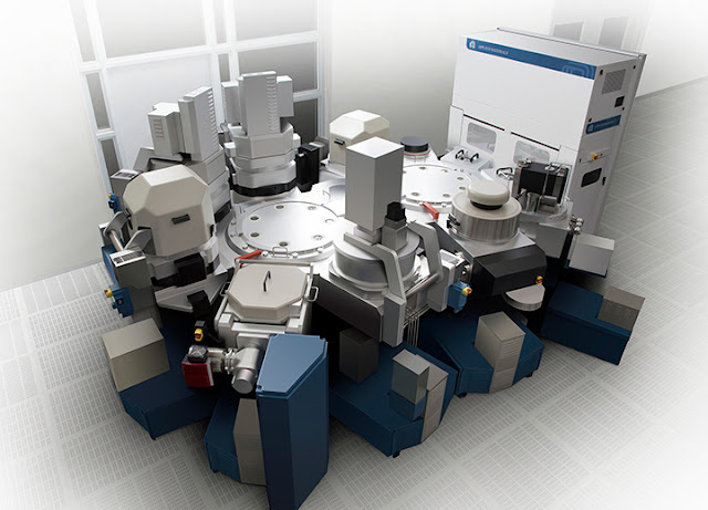
The joint lab features several of Applied Materials’ 200mm and 300mm wafer processing systems, such as this Endura® system, and leverages CEA-Leti’s world-class capabilities for evaluating performance of new materials and device validation.
The collaboration aims to enhance power efficiency, performance, and cost-effectiveness, while also reducing time to market. Aninda Moitra, corporate vice president and general manager of Applied Materials' ICAPS business, emphasizes this initiative as an extension of a decade-long successful partnership, geared towards accelerating innovation in specialty semiconductor technologies.
Sébastian Dauvé, CEO of CEA-Leti, reflects on the decade of collaborative projects leading up to this new joint lab. These projects spanned advanced metrology, memory materials, optical devices, bonding techniques, and chemical-mechanical planarization. The results have consistently delivered high value, setting a solid foundation for this expanded engagement.
The lab not only aims to develop unique technological solutions for Applied Materials' customers but also supports CEA-Leti's internal R&D programs, overcoming current technical challenges. This initiative marks a significant step in the collaboration, promising to bring breakthroughs in specialty semiconductor technology to global markets.


%20(1).png)

The collaboration aims to enhance power efficiency, performance, and cost-effectiveness, while also reducing time to market. Aninda Moitra, corporate vice president and general manager of Applied Materials' ICAPS business, emphasizes this initiative as an extension of a decade-long successful partnership, geared towards accelerating innovation in specialty semiconductor technologies.
ReplyDelete