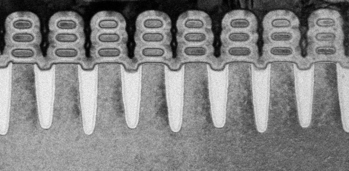
Friday, June 16, 2017

Advanced Materials Special Issue: Materials Platform at Aalto University

Aalto University Reports (LINK):Advanced Electronic Materials, an academic peer-reviewed high-impact materials science journal, has published a special issue dedicated to materials research at Aalto University, in Espoo (near Helsinki), Finland.


Link to special issue: http://onlinelibrary.wiley.com/doi/10.1002/aelm.201770023/full

Some selected papers interestig for the Atomic Layer Community:

Ozone-Based Atomic Layer Deposition of Al2O3 from Dimethylaluminum Chloride and Its Impact on Silicon Surface Passivation - Yameng Bao,* Mikko Laitinen, Timo Sajavaara, and Hele Savin

Band Bending Engineering at Organic/Inorganic Interfaces Using Organic Self-Assembled Monolayers - Oliver T. Hofmann* and Patrick Rinke

Flexible Thermoelectric ZnO-Organic Superlattices on Cotton Textile Substrates by ALD/MLD - Antti J. Karttunen,* Liisa Sarnes, Riikka Townsend, Jussi Mikkonen, and Maarit Karppinen

Enhanced p-Type Transparent Semiconducting Characteristics for ALD-Grown Mg-Substituted CuCrO2 Thin Films - Tripurari S. Tripathi and Maarit Karppinen*


Wednesday, June 14, 2017

LATE POSTER: 20170614 Process development of ALD and CVD of MoOx and MoS2 employing Mo(CO)6

Here is a LATE POSTER, 20170614 for EuroCVD-BalticALD 2017 in Linköping - Process development of ALD and CVD of MoOx and MoS2 employing Mo(CO)6.


VTT Finland method accelerates the development of microelectronics in three dimensions

Press Release: VTT Technical Research Centre of Finland has developed the unique PillarHall test structures to accelerate the market entry of three-dimensional, small, efficient and low-power but high-performance electronic components. This will benefit developers of challenging thin film and related manufacturing processes, and thereby the entire electronics industry value network.

There has been occasional speculation on whether Moore's Law remains valid. Transistors are already being packed into squares so small that their rate of shrinkage is accelerating in three dimensions. For example, the equivalent of 4 billion 72-storied skyscrapers on a dime has enabled the creation of a 256 GB memory chip.

Picture source VTT Finland Media release.

VTT has developed record-high aspect ratios on an extremely challenging scale (10,000:1 and 100 nm) for the 3D test structures on silicon chips and wafers, to meet the requirements of the most challenging applications. Such applications include in addition to semiconductor circuits, also optics, MEMS, sensors, thin film batteries and photovoltaics.

"What makes our chips special is that we have turned the analysis 90 degrees and adopted a lateral rather than the traditional vertical approach, which enables much faster data production and lead times than current methods. For example, cross-sectional analysis of microscopic vertical structures can take weeks, whereas Pillar Hall provides data without delay. Other advantages include accuracy, versatility and compatibility with varying process conditions," says inventor and Senior Scientist Riikka Puurunen (D.Sc. (Tech.)) of VTT.

The PillarHall test structure also introduces a new parameter space into the analysis, which allows more efficient thin-film R&D, adoption of new industrial applications and process control.

PillarHall is being funded under Tekes' Research Commercialisation Programme. This involves developing silicon chips for quantifying thin-film conformality, which is a key value proposition of ALD (Atomic Layer Deposition) technology. ALD has originally been developed in Finland and Finland's key ALD technology players are involved in the Project Advisory Group: ASM, Beneq, Picosun, the University of Helsinki and Okmetic Oy.

VTT is currently working with PillarHall's 3rd-generation prototypes, which have been successfully tested by Finnish partners and a number of research institutes. VTT is now seeking international partners, in particular, as test users to push forward with the testing and commercialisation of the chips.

"The interest shown by industry and the positive experiences of users build confidence in our vision that PillarHall chips and wafers could one day become the conformality standard and be commercially available," says Project Manager Mikko Utriainen (D.Sc. (Tech.).

More information about the project:

http://pillarhall.com

VTT Blog: Moore's law - is it a spring of productivity? https://vttblog.com/2017/05/30/moores-law-is-it-a-spring-of-productivity/

Day 3 (Tuesday) EuroCVD-Baltic ALD 2017 in Linköping, Sweden

Here is a collection of tweets from Day 3 (Tuesday) EuroCVD-Baltic ALD 2017 in Linköping; Sweden.


Atomic Scale Processing Webinar with Oxford Instruments

Last chance to register! FREE webinar tomorrow:
Atomic Scale Processing | 15th June, 3:30pm BST


In this webinar, our experts Dr Ravi Sundaram and Dr Harm Knoops discuss the processing of atomic scale materials and devices including Graphene and 2D materials, atomic layer etching and atomic layer deposition. The webinar will comprise of two talks, with a Q&A session at the end:

• Atomic scale processing: Atomic Layer Deposition & Etching
Dr Harm Knoops

• Processing of atomic scale materials & devices: Graphene & 2D
materials | Dr Ravi Sundaram


Tuesday, June 13, 2017

Atomic layer deposition for device integration of graphene (Review)

Just published by Prof. Kessels: A brief and easy-to-read synopsis of our new review paper about ALD for device integration of graphene as published in Advanced Materials Interfaces (Atomic Layer Deposition for Graphene Device Integration, 26 May 2017, DOI: 10.1002/admi.201700232).

Atomic Limitts Blog: LINK

Picture from AtomicLimits.com


Day 2 (Monday) EuroCVD-Baltic ALD 2017 in Linköping, Sweden

Here is a collection of tweets from Day 2 (Monday) EuroCVD-Baltic ALD 2017 in Linköping; Sweden.

First invited speaker of Martin Magnusson from on aerotaxy.


Monday, June 12, 2017

Atomic Layer Deposition Market Set to Cross USD 5 Billion by 2022 at a CAGR of 31.27%

According to the new report, “Atomic Layer Deposition Market - By Type (Equipment & Materials); By Application (Gate Dielectrics, Gate Electrodes, Metal Interconnects, Diffusion Barriers, Memory Chips, Multilayer Capacitors, OLED Layers, Solar Cells, Fuel Cells, MEMS and Others); By Geography – Forecast (2016-2022)”, published by IndustryARC, the atomic layer deposition market to cross USD 5 Billion by 2022 at a high CAGR.


Atomic Layer Deposition in increasingly being used in manufacturing of electronic products where thickness of the film is absolutely imperative such as; smart phones, printers, data storage devices, displays, different types of small electronic components and many others products. It is mainly responsible for semiconductor fabrication and nanomaterial synthesis. Growing application of thin film coatings is the major driving factor for atomic layer deposition market. Through atomic layer deposition, ultra-thin films can be created in a sequential and self-limiting way depending on the material or product, which needs the layer to be applied on. Atomic layer Deposition process is especially favored because of its ability to control the film thickness in nanometer thickness regime. Atomic layer deposition is a perfect deposition method for applications where the surface area of the base material is very small.

According to a recent study from IndustryARC the global market value of atomic layer deposition was $910 million in 2015. Atomic layer deposition instruments are expensive as compared to conventional techniques such as MOCVD and PVD, consequently the equipment used for atomic layer deposition accounted for more than 60% of the global market revenue share.

Inquiry before Buying Report @ http://www.industryarc.com/inquiry-before-buying.php?id=15340

Day 1 (Sunday) EuroCVD-Baltic ALD 2017 in Linköping; Sweden

Here is a collection of tweets from Day 1 (Sunday) EuroCVD-Baltic ALD 2017 in Linköping; Sweden.


Thursday, June 8, 2017

Solar conversion of CO2 by ALD modified CuO catalyst


Chemistry World reports that Earth abundant materials can be nano-engineered to make best use of increasingly abundant solar power. Now researchers in Switzerland have developed a catalyst, made entirely from earth abundant materials, that allows solar-generated electricity to reduce the environmental pollutant carbon dioxide to the valuable chemical feedstock carbon monoxide.

In the new research, Luo and colleagues used atomic layer deposition – a modified form of chemical vapour deposition allowing deposition of single, continuous atomic layers – to cover copper oxide nanowires with a very thin layer of tin oxide. Please find more detailed information and sources below

Full story:  LINK

Reference:
M Schreier et al, Nat. Energy, 2017, 2, 17087 (DOI: 10.1038/nenergy.2017.87)

Abstract: The solar-driven electrochemical reduction of CO2 to fuels and chemicals provides a promising way for closing the anthropogenic carbon cycle. However, the lack of selective and Earth-abundant catalysts able to achieve the desired transformation reactions in an aqueous matrix presents a substantial impediment as of today. Here we introduce atomic layer deposition of SnO2 on CuO nanowires as a means for changing the wide product distribution of CuO-derived CO2 reduction electrocatalysts to yield predominantly CO. The activity of this catalyst towards oxygen evolution enables us to use it both as the cathode and anode for complete CO2 electrolysis. In the resulting device, the electrodes are separated by a bipolar membrane, allowing each half-reaction to run in its optimal electrolyte environment. Using a GaInP/GaInAs/Ge photovoltaic we achieve the solar-driven splitting of CO2 into CO and oxygen with a bifunctional, sustainable and all Earth-abundant system at an efficiency of 13.4%.

NC State show ALD enhanced zirconia MOFs for protective clothing against chemical weapons

ScienceDaily reports: Since their first use in World War I and most recently by the Assad regime in Syria, chemical weapons with devastating potential have been developed. Therefore scientists have begun exploring the use of zirconium-based metal-organic framework (MOF) powders to degrade and destroy these harmful compounds.
  • Zirconium Asists in neutralizing toxic materials. 
  • MOF powders are unstable and incorporating them onto clothing has proven challenging. 
Therefore Dennis Lee, Gregory N. Parsons et al has investigated growth of MOFs onto fabric at room temperature, which potentially could realize protection by being coated on to uniforms and other protective clothing.


The researchers developed a process were the a fine fabric (nonwoven) commonly used in reusable shopping bags and some clothing is exposed polypropylene, followed by another exposure to a to a mixture consisting of a zirconium-based MOF, a solvent and two binding agents.

Finally, to make sure that the active zirconia MOF-coating spread evenly across the cloth, they treated the fabrics with thin ALD layers of aluminum, titanium or zinc oxide. They tested this combination with dimethyl 4-nitrophenyl phosphate (DMNP), a relatively harmless molecule that has similar reactivity as sarin, soman and other nerve agents.

They found that the MOF-treated cloths deactivated DMNP (a Sarin like compound) in less than 5 minutes, suggesting this process is a viable means to create improved protective clothing.


References:

American Chemical Society. "New fabric coating could thwart chemical weapons, save lives." ScienceDaily. ScienceDaily, 7 June 2017. www.sciencedaily.com/releases/2017/06/170607123930.htm.

Dennis T. Lee, Junjie Zhao, Gregory W. Peterson, Gregory N. Parsons. Catalytic “MOF-Cloth” Formed via Directed Supramolecular Assembly of UiO-66-NH2 Crystals on Atomic Layer Deposition-Coated Textiles for Rapid Degradation of Chemical Warfare Agent Simulants. Chemistry of Materials, 2017; DOI: 10.1021/acs.chemmater.7b00949

Wednesday, June 7, 2017

Another breakthrough in CMOS-compatible ferroelectric memory

Imec, the world-leading research and innovation hub in nanoelectronics and digital technology, announced today at the 2017 Symposia on VLSI Technology and Circuits the world's first demonstration of a vertically stacked ferroelectric Al doped HfO2 device for NAND applications. Using a new material and a novel architecture, imec has created a non-volatile memory concept with attractive characteristics for power consumption, switching speed, scalability and retention. The achievement shows that ferro-electric memory is a highly promising technology at various points in the memory hierarchy, and as a new technology for storage class memory. Imec will further develop the concept in collaboration with the world's leading producers of memory ICs.

Full story : LINK

Monday, June 5, 2017

IBM, Samsung and Globalfoundries shows off the world´s first 5 nm logic chip with GAAFETs

IBM together with Samsung and Globalfoundries shows off the world´s first 5 nm logic chip with horizontal Gate All Around Field Effect Transistors also referred to as GAAFETs. GAAFETs are a evolutionary development out of FInFETS that were fisrt introduced at 22 nm by Intel. It is predicted that 7 nm will be the last FinFET node and that GAAFETs has to be introduced by then.

Source: IBM LINK

 TEM cross section of 5nm GAAFETs by IBM, Samsung and Globalfoundries (Source IBM)

The GAAFETs are manufactued by deposition stacks of epitaxial silicon and silicon germanium (Si/SiGe Epi). Then by using a combination of EUV lithography and reportedly (LINK) Atomic Layer Etching (ALE) trenches are etched to separate the stack into fins and then afterwards to individual nanowires (or nano sheets as IBM calls them) of Si resp SiGe forming the channels stacked on top of each other. Later the high-k / metal gate (HKMG) stack is deposited in by a sequence of ALD processes conformally covering the nanowire channels.


In the nano sheet FETs, the wires are much wider and thicker presumably giving the nano sheet FETs better electrostatics and drive current

Articles :

Want a smarter phone? IBM and Samsung bring you: Nanosheets!
CNET
If you're frustrated with smartwatches that aren't that smart or phones that don't pack enough power, IBM and Samsung have some good news ...


Sunday, June 4, 2017

EpiValence is sposnoring Best Student Awards at EuroCVD-Baltic ALD 2017 in Sweden

I just a week the EuroCVD-Baltic ALD 2017 conference kicks off in Linköping, Sweden (11-14th of June). Right now many students are putting their final touches to their presentations and posters and to motivate you even more we have a treat for you!


Epivalence is sponsoring the best student poster and best student presentation prices, which will be given at the conference dinner. You can meet Equivalence in the Industry exhibition at the conference.

Thursday, June 1, 2017

Pushing the Bounds of Nanoscale Processing at 'Nanotech 2017: Pushing the Limits' Workshop

Oxford Instruments and the Kavli Nanoscience Institute at the California Institute of Technology (CALTECH) are holding a one day workshop on 19th July 2017.

This workshop will explore recent progress in nanoscale plasma processing research and development, plus looking at future trends in the fabrication and application of micro, nano and atomic scale structures and devices.

Source: AZoNano LINK


Wednesday, May 31, 2017

Extended Deadline for Abstracts E-MRS 2017 Fall Meeting

E-MRS 2017 Fall Meeting Final Call [PDF] About E-MRS Contact
E-MRS 2017 Fall Meeting
Extended Deadline for Abstracts
The 2017 E-MRS Fall Meeting and Exhibit will be held
in Warsaw University of Technology
from September 18th to 21st - Monday-Thursday
The conference will include 23 parallel symposia,
one plenary session, one exhibition
and much more;
New Abstract deadline: June 5th, 2017

ALD barrier improves stability of perovskite quantum dots

EPFL Reports: A new approach to stabilize perovskite quantum dots has been developed in the lab of Raffaella Buonsanti at EPFL Valais Wallis. ALD was used to encapsulate the perovskite quantum dots with an amorphous alumina matrix, which acts as a gas and ion diffusion barrier making the quantum dots more robust against air, light, heat, and moisture.


Reference paper: A. Loiudice, S. Saris, E. Oveisi, D. T. L. Alexander, R. Buonsanti. CsPbBr3 QD/AlOx inorganic nanocomposites with exceptional stability in water, light and heat. Angewandte Chemie 26 May 2017. DOI: 10.1002/anie.201703703

According to the publication an Ultratech/CNT Savannah 200 ALD was used to process the Al2O3 barrier. Please fin all the details in the supporting information (LINK) as well as a movie showing the accelerated test in a water bath (LINK)

Tuesday, May 30, 2017

The AVS ALD2017/ALE2017 schedule and book of abstracts is now available online

The AVS ALD2017/ALE2017 schedule and book of abstracts is now available online & technical program:  


The AVS 17th International Conference on Atomic Layer Deposition (ALD 2017) featuring the 4th International Atomic Layer Etching Workshop (ALE 2017)  will be a three-day meeting dedicated to the science and technology of atomic layer controlled deposition of thin films and now topics related to atomic layer etching. Since 2001, the ALD conference has been held alternately in the United States, Europe and Asia, allowing fruitful exchange of ideas, know-how and practices between scientists. This year, the ALD conference will again incorporate the Atomic Layer Etching 2017 Workshop (ALE 2017), so that attendees can interact freely. The conference will take place Saturday, July 15-Tuesday, July 18, 2017, at the Sheraton Downtown Denver in Denver, Colorado, USA. 

Monday, May 29, 2017

Picosun reports repeat sales of production cluster systems

ESPOO, Finland, 29th May, 2017 – Picosun Oy, leading supplier of advanced Atomic Layer Deposition (ALD) thin film coating technology, reports of repeat sales of PICOPLATFORM™ production cluster systems to major industries.

The PICOPLATFORM™ cluster systems are designed for fully automated, high throughput operation in production environment. Several leading microelectronics manufacturers in USA and Asia have chosen these systems to manufacture IC components in the most advanced semiconductor nodes. The SEMI S2/S8 compatible PICOPLATFORM™ systems can handle wafers up to 300 mm size. The modular configuration with a comprehensive variety of wafer handling automation systems ensures each PICOPLATFORM™ cluster can be tailored for optimal performance according to each customer’s individual needs, whereas fast processing ensures low cost of ownership. To maximize system uptime and to guarantee always flawless process quality, Picosun provides all-inclusive after sales support, including precursor delivery services, through PicoSupport™ and PicoDevelopment™ service contracts and programs.

“We are proud of the confidence that our industrial customers place on us. Today, we collaborate with the global tier one businesses in semiconductor manufacturing. These companies are leaders in their own fields and possess the highest expertise in what they do, but when it comes to ALD, it’s Picosun in whom they trust. Repeated sales of production cluster systems to these companies proves our ability to satisfy even the most stringent demands of semiconductor industry leaders,” states Mr. Kustaa Poutiainen, Chairman of the Board and Chief Executive Officer of Picosun.

Saturday, May 27, 2017

Argonne scientists uses ALD vanadium as a catalyst for hydrogenation

Argonne researcher Max Delferro enhanced a process for catalytic activity of  vanadium for hydrogenation. The advantage is that if we can make vanadium that is an abundant metal catalytically active there are huge cost savings compared to using noble metals like Platinum or Paladium.

“Getting single-atom vanadium into this special configuration on metal oxide surfaces is not easy,” Delferro said. “It requires the use of special synthetic techniques such as surface organometallic chemistry and atomic layer deposition. However, if we can make vanadium or another abundant metal as catalytically active as the noble metals, we can create dramatic cost savings in these very common and commercially important catalytic processes.” Delferro said in a press release by Argonne (LINK).


Check out the new branding of Picosun - Agile ALD Solutions

Check out the new branding of Picosun - Agile ALD Solutions! (LINK)


You can meet Picosun exhibiting on the follwing upcming events:

June 11 - 14 Linköping, Sweden
EuroCVD-21 – BalticALD-15 

July 11 - 13 San Francisco, CA, USA
Semicon West 2017 (booth # 7121) 

July 15 - 18 Denver, CO, USA
ALD 2017 – The 17th International Conference on Atomic Layer Deposition (booth # 8-9) 

September 13 - 15 Taipei, Taiwan
Semicon Taiwan 2017

Veeco Completes Acquisition of Ultratech

Thin-film etch and deposition process equipment maker Veeco Instruments Inc of Plainview, NY, USA has completed its acquisition of Ultratech Inc of San Jose, CA, USA (which designs and makes lithography, laser-processing and inspection systems used to manufacture semiconductor devices and LEDs...


Source: Semiconductor Today
Read full article >

Friday, May 26, 2017

ALD & Synchotron Radiation at e-MRS 2017, fall meeting in Warsaw

Information from the symposium chairs Malgorzata Kot, Claudia Wiemer, Gianluca Ciatto and Joachim Schnadt: The deadline for abstract submission to e-MRS 2017, fall meeting, is approaching, please consider to submit an abstract to:

SYMPOSIUM Q: "SYNCHROTRON RADIATION AND ATOMIC LAYER DEPOSITION FOR ADVANCED MATERIALS"

Please visit the symposium website at
http://www.european-mrs.com/synchrotron-radiation-and-atomic-layer-deposition-advanced-materials-emrs

abstract submission deadline: Monday, May 29th!

Hot topics to be covered by the symposium:
  • Characterization of ALD processes and materials (metals, oxides) using synchrotron light (PES, XANES, EXAFS, GISAXS, XRD, XRR, XRF, etc.)
  • Investigation of ALD film nucleation, interface properties and growth by laboratory-based tools
  • In situ/operando monitoring of ALD processes (APXPS, infrared spectroscopy, etc.)
  • Modeling of the Atomic Layer Deposition
  • ALD method types (thermal, plasma and electron enhanced, spatial, etc.) 
  • Application of ALD (solar cells, LED, HEMT, MIM capacitors, LMR silica-fiber sensors, GaN power devices, TSV field effect transistor, MEMS, etc.)


Aixtron to sell its ALD/CVD business to Eugene Technology


Aixtron will sell the ALD and CVD memory product line, at Aixtron, Inc. based in Sunnyvale, California to Eugene Technology Inc., a wholly owned U.S. subsidiary of Eugene Technology Co., Ltd, South Korea.

Source: Evertiq
Read full article >

Aixtron completed take over of American ALD/CVD rival Genus, Inc. in March 2005 for about USD 140 million. This deal is reported to be in the order of USD 45 million and 55 million, which is considerably less.

Reportedly, the main customer today for Aixtron ALD is Samsung and the Aixtron ALD/CVD semiconductor business unit has had an annual revenue at about USD 20 to 40 million the last years years.


Thursday, May 25, 2017

International Training School on Atomic Layer Deposition - ALD-UKRAINE 2017

At this training workshop, top class experts from top research laboratories around the world will share their knowledge and experience in ALD, reviewing the current trends for R&D organizations.
Atomic layer deposition (ALD) – is a unique technique that allows to develop and implement numerous emerging technologies in such fields as: micro-nano(opto) electronics, flexible electronics, anti-corrosion surfaces, biocompatible coatings for biomedical applications, textiles, implantology, self-cleaning coatings, etc. Since Ukraine is represented in all these fields, ALD-UKRAINE 2017 is a beneficial event for research and industrial community that can lead Ukrainian R&D institutes and enterprises to a new level of development.


The event is organized by the HERALD COST Action and the Institute of Microdevices (NAS of Ukraine) in collaboration with Igor Sikorsky Kyiv Polytechnic Institute and IEEE Ukraine Section. For more information please check out the event website
Dates: 30 May 2017 to 1 Jun 2017 

Organising Members:
Simon Elliott
Petro Deminskyi

Samsung Display Unveil World’s First ‘Stretchable’ OLED Panel

Business Korea reports: Samsung Display announced on May 22 that it will showcase its advanced future display products which have never been revealed such as stretchable display, glasses-free 3D organic light-emitting diode (OLED) and ultra-high-definition LCD display that features 2,250 pixels per inch (ppi), at the Society for Information Display (SID) 2017, which will be held at the Los Angeles Convention Center from May 23 to 25 (local time).


The most striking exhibit from Samsung at the event will be a 9.1-inch stretchable OLED display. The product is a next generation display technology that can be flexibly stretched. It is considered the future technology that fits the most for wearable, Internet of Things (IoT) and artificial intelligence (AI) devices as well as automotive displays.

Full story:  LINK

Updated website PillarHall for ALD conformality test structures

Updated website PillarHall for ALD conformality test structures : http://www.pillarhall.com


MV Products' Vacuum Inlet Traps Protect Atomic Layer Deposition Tools

North Billerica, MA (PRWEB) May 24, 2017 MV Products has introduced a full line of vacuum pump inlet traps that can be customized by users to protect the vacuum pumps and lines on atomic layer deposition (ALD) tools from particulates and unreacted precursors.

MV Vacuum Inlet Traps for ALD processes can be easily customized by users to remove all process byproducts from precursors such as TMA, TiCl, DeZ, and H2S including particulates and unreacted precursors. Suitable for the manufacturing of ICs, MEMS, LEDs and OLEDs, optics, displays, batteries, and more, these stainless steel traps are offered in sizes for protecting vacuum pumps and lines with flow rates from 25 to 2000 CFM. 
 
The MV MULTI-TRAP® is a high capacity, high conductance vacuum inlet trap that protects your pump against corrosive chemicals and abrasive particles present in your vacuum system (MV Vacuum Inlet Traps ).
 
Available for both research and production applications, MV Vacuum Inlet Traps for ALD processes Traps range from 4" to 16" dia. with port sizes from NW-25 to ISO-160 and use interchangeable filter elements. Filter types include stainless steel gauze for particle filtration, activated charcoal for unreacted cursor adsorption, Sodasorb® for acid neutralization, and Sulfatreat® for H2S neutralization.

MV Vacuum Inlet Traps for ALD processes are priced from $249.95 to $4,799.00, depending upon configuration. Price quotations are available on request.

Thursday, May 18, 2017

Oxford Instruments are promoting a cluster tool for Atomic Scale Processing

Oxford Instruments are promoting a cluster tool for Atomic Scale Processing including the metrology tools to analyze and monitor these processes:
Metrology:


The technology exists to make these layers and Plasma Technology has these tools and is uniquely able to cluster them all on a single tool (LINK).

Tuesday, May 16, 2017

Welcome to the 2nd ALD Fest by ALD Lab Saxony 23rd of May in Dresden

Welcome to the 2nd ALD Fest by ALD Lab Saxony! We are also very happy to announce a new partner Picosun and welcome more insudtry partners to join us!

Agenda of ALD Lab Meeting on Tuesday 23rd of May 2017

Contact: jonas.sundqvist@ikts.fraunhofer.de (Mobile +49 152 0294 3083)

Part 1 - Presentations and discussions 17:00 till 19:00

Place: Fraunhofer IKTS, Winterbergstrasse 28, 01277 Dresden
  • Review ALD For Industry, Jonas Sundqvist and Christoph Hossbach 
  • Review of Novel High-k Workshop, Uwe Schröder 
  • Review von Critical Materials Conference – CMC2017, Dallas 11-12 May, Jonas Sundqvist Feedback and Future of HERALD – The European ALD Network, Marcel Junige
Presentation of new partner
  • Picosun presentation – new member, Christoph Hossbach 
Discussion
  • Things we are able to offer as a network/division within Cool Silicon e.V.
  • Plans for the future and conferences (EuroCVD, ALD2017, EFDS ALD For Industry 2018).
Travel information:
 German: https://www.ikts.fraunhofer.de/de/contact/anfahrtdd.html
 English: https://www.ikts.fraunhofer.de/en/contact/anfahrtdd.html

Part 2 - Joint dinner and networking 19:00 till 23:00

Place: Hotel und Restaurant an der Rennbahn, Winterbergstrasse 96, 01237 Dresden; in walking distance to IKTS

Travel information:
German: http://www.hotel-an-der-rennbahn-dresden.de/lage-anreise/
English: http://www.hotel-an-der-rennbahn-dresden.de/en/lage-anreise/