


%20(1).png)
2016 will be another growth year for OEM stocks and Atomic Layer Processing. In a report recently published by JP Morgan, analysts predicted another growth year in 2016 for Semiconductors stocks, driven by technology transitions in memory and 10nm FinFET. So this is good news for all Tier 1 OEMs with a number of ALD and ALE technologies in the game.
Technology transitions by memory companies :
- continued 3D NAND ramps
- additional 20nm conversions
- initial 1Xnm DRAM deployments
- deploying FinFET technologies (especially 10nm FinFET)
- multi-patterning steps and vertical transistors
"In general, we see capital intensity increasing by 10-15% on a per wafer basis when transitioning from 14nm/16nm FinFET to 10nm FF and by 15+% when transitioning to 20nm and below DRAM / 3D NAND. The number of critical patterning layers is increasing dramatically – in the foundry/logic segment, the number of critical layers is increasing by over 3x going from 28 nm node to the 10nm node…a significant increase," the analysts added.Read more: http://www.benzinga.com/analyst-ratings/analyst-color/15/05/5488523/jp-morgan-sees-another-growth-year-for-semiconductors-th#ixzz3aNRgk5q0
Below is an overview of some of the ALD and ALE technologies offered by the leading OEMs. It is ion sense complete yet so please let me know what is missing (jonas.sundqvist@baldengineering.com).
LAM Research

LAM Research reported in 2014 that "The latest in Lam's market-leading tungsten deposition product line, the ALTUS Max ICEFill system controls variability by providing void-free fill of the geometrically complex 3D NAND wordlines. Using a proprietary filling technique, the new system creates the tungsten wordlines with an inside-out atomic layer deposition (ALD) process. The ICEFill process completely fills the lateral (horizontal) lines without any voids, while at the same time minimizing deposition in the vertical channel area. As a result, both electrical performance and yield are enhanced."

Lam’s ALTUS systems combine CVD and ALD technologies to deposit the highly conformal films needed for advanced tungsten metallization applications (http://www.lamresearch.com/products/deposition-products).
Lam's new ALE capability on the 2300 Kiyo F Series conductor etch system provides both the productivity and technology needed. The product leverages fast gas switching and advanced plasma techniques in the reactor to boost throughput, while dynamic RF bias enables the directional etching required to remove material in high aspect ratio (deep and narrow) features. As the latest offering in Lam's market-leading Kiyo family, the 2300 Kiyo F Series system continues to provide superior uniformity and repeatability enabled by a symmetrical chamber design, advanced electrostatic chuck technology, and independent process tuning features.

- Shallow trench isolation
- Source/drain engineering
- High-k/metal gate
- FinFET and tri-gate
- Double and quadruple patterning
- 3D NAND
To learn how atomic layer deposition (ALD) and atomic layer etch (ALE) processes work, watch this video from LAM Research (www.youtube.com).
Applied Materials
CENTURA® ISPRINT™ TUNGSTEN ALD/CVD - The Applied Centura iSprint Tungsten ALD/CVD system provides complete contact/via fill for structures with aspect ratios ranging from 4:1 to 7:1 and extends the capability of tungsten technology to 20nm/16nm for logic and memory applications.

The iSprint system also delivers high throughput and low cost of consumables with an optimized ALD chamber design featuring a proprietary rapid gas delivery system and small chamber volume that enable fast, effective gas purging that uses less gas (www.appliedmaterials.com).
CENTURA® INTEGRATED GATE STACK - The system consists of an ALD HfO2 (hafnium oxide) deposition chamber and specialized chambers for interface layer oxide formation, post high-k nitridation, and post-nitridation anneal

The Centura Integrated Gate Stack system with ALD high-k chamber technology for 22nm and below uses Applied’s production-proven Centura Gate Stack platform to deliver the complete high-k process sequence in a controlled high vacuum environment without an “air break” (www.appliedmaterials.com).
Tokyo Electron
Tokyo electron has a number of ALD technologies and are very strong in batch processing that is used to large extent in DRAM production to get the cost per wafer down since DRAM is a commodity product.
- TEL Formula - Mini batch, thermal processes including ALD for High-k, SiO2, SiN.
- TEL INDY Plus - Large batch, thermal processes including ALD for High-k, SiO2, SiN.
- TEL INDY IRad - Large batch, PEALD for ultra low temperature SiO2 and SiN.
- TEL NT333 - Single wafer cluster tool for high t-put SiO2.
TEL INDY Large batch furnace for thermal processing and ALD (www.tel.com)

The NT333 applies inherent ALD concepts against conventional ALD processing to address the critical performance needs imposed by aggressive geometries. The NT333 can effectively deposit with a very tight thickness control, a range of less than 1A, while maintaining a productivity of 100+ wafers per hour. With a very unique reactor design, each of the ALD duty cycles enables the NT333 to deliver the high film quality which is typically compromised at low temperature regimes (<400C). (www.tel.com)
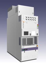
ASM International
ASM's ALD technologies, includes thermal ALD (Pulsar) for FinFET high-k metal gate stacks, and various applications of Plasma Enhanced ALD (Emerald) as an enabler for low temperature processing such as multiple patterning on resist and deposition of doped silicon oxide for solid state doping of FinFETs.

ASM’s Pulsar uses ALD to deposit the high-k dielectric materials required for advanced CMOS transistor gates and other applications. Pulsar is the benchmark ALD high-k tool for the industry. It was the first ALD system to be used for high-volume production at advanced customers for high-k metal gate transistors (www.asm.com).

EmerALD XP is a process module designed to deposit thin conformal metal and dielectric layers by atomic layer deposition (ALD) used for advanced CMOS gate stacks and other applications (www.asm.com).

Eagle XP8 is a high productivity 300mm tool for PEALD applications. The Eagle XP8 PEALD system can be configured with up to four Dual Chamber Modules (DCM), enabling eight chambers in high volume production within a very compact footprint (www.asm.com).
ASM Chip Making Process (www.youtube.com)
You have done good work by publishing this article here.Multi Walled Carbon Nanotubes India I found this article too much informative, and also it is beneficial to enhance our knowledge. Grateful to you for sharing an article like this.
ReplyDelete