- Lam Research: $800 - now $717
- ASM International: €545 - now $459
- KLA: $550 - now $554
- Applied Materials: $175 - now $149
Thursday, November 23, 2023
AI-Driven Chip Demand Spurs Optimism in Semiconductor Industry; Analyst Upgrades Key Players with Bullish Price Targets
Wednesday, November 22, 2023
SEMICON Europa 2023: A Deep Dive into ALD Technology for Wafer Fab Equipment in the More-than-Moore Era
Last week at SEMICON Europa, at the ALD Tech Day Organized by Beneq, Yole Group presented a comprehensive analysis on ALD technology for More-than-Moore (MtM) devices, focusing on its impact and future in the wafer fab equipment market. The presentation titled "Atomic Layer Deposition for More-than-Moore Devices in a Perspective of the Wafer Fab Equipment Market" offered valuable insights into the current trends and future directions of this pivotal technology.
The Growing Importance of ≤200 mm Wafers
A focal point of the discussion was the ≤200 mm wafer size, a segment that remains crucial in the semiconductor industry despite the surge in larger wafer sizes. The presentation highlighted the market size, chipmaker revenue, and capacity expansion specifically for this category. It emphasized that while the industry continues to evolve technologically, the demand for ≤200 mm wafers remains robust, accounting for a significant portion of the market.
Semiconductor Device Revenue Projections
Yole Group presented a detailed forecast for semiconductor device revenue, segmenting it by device type. They projected a CAGR of approximately 4.5%, expecting the overall market to reach around $850 billion by 2030. Within this, MtM devices are anticipated to contribute significantly, estimated at about $270 billion, indicating the growing relevance of these devices in the semiconductor landscape.
Capital Expenditure Trends and ALD Market Dynamics
The presentation also shed light on the capital expenditure (CapEx) trends in the industry, particularly for 200 mm wafer processing. With CapEx projected to increase to 17% of the revenue by 2025, a subsequent trend towards more sustainable levels by 2028 was also anticipated. This trend underscores the expanding market and the need for more Wafer Fab Equipment (WFE), presenting a substantial opportunity for the growth of ALD technologies.
Atomic Layer Deposition: Meeting Industry Needs
The analysis delved deeply into the ALD market, discussing how this technology is evolving to meet the changing demands of the semiconductor industry. It was pointed out that ALD technology is not just adapting but also driving significant advancements, particularly in the context of MtM devices.
From the presentation by Yole Group focuses on the use of ALD in power devices, emphasizing its role in enhancing device performance through precise interface control. The need for specialized ALD equipment, capable of handling multiple processes and materials, including thermal and plasma ALD with various precursors. ALD applications are found in in Silicon Carbide (SiC) and Gallium Nitride (GaN) devices, covering aspects like passivation, substrate creation, and buffer layers. While ALD is still in R&D for GaN High Electron Mobility Transistors (HEMT), it is already being used for SiC Trench and Planar MOSFETs in encapsulation and gate dielectrics, signaling its growing importance in semiconductor manufacturing.
Industry Challenges and Opportunities
The challenges and opportunities within the semiconductor industry were a crucial part of the discussion. The presentation addressed the current supply chain dynamics, technological innovations, and market trends that are shaping the adoption and development of ALD technology.
Conclusion
The presentation at SEMICON Europa provided a lucid and detailed perspective on the ALD technology in the context of the wafer fab equipment market. With a focus on ≤200 mm wafer size, it painted a comprehensive picture of the current market scenarios, future trends, and the pivotal role of ALD technology in shaping the future of semiconductor manufacturing. As the industry continues to evolve, the insights from this presentation will undoubtedly influence strategic decisions and technological advancements in the semiconductor sector.
Source: ALD TECHDAY 2023 powered by Beneq (yolegroup.com)
Presentation shared with the attendees
AIXTRON's G10-GaN System Empowers BelGaN's Expansion into the Growing GaN Semiconductor Market
The article discusses AIXTRON's support for BelGaN in expanding its Gallium Nitride (GaN) business through the new G10-GaN system. AIXTRON SE, a semiconductor company, is enabling BelGaN, a leading GaN automotive-qualified semiconductor foundry in Europe, to enter the growing GaN market and boost GaN technology innovation. BelGaN plans to use AIXTRON's G10-GaN, which offers top performance, a compact design, and low cost per wafer, starting with an 8x150mm configuration, to be delivered to BelGaN's production site in Oudenaarde, Belgium, by the end of 2023. This system will later evolve to support 5x200mm.
AIXTRON's G10-GaN System Empowers BelGaN's Expansion into the Growing GaN Semiconductor Market
BelGaN aims to expand its power chip range with voltage ratings from 40V to 1200V, utilizing GaN-on-Si, GaN on SOI, and new GaN-on-engineered substrates, focusing on high performance, automotive quality, reliability, high yield, and low costs. The G10-GaN will enable innovations in device architectures and improvements in performance, yield, and quality, reducing the cost of GaN products. This advancement is expected to drive growth in e-mobility, datacom, energy conversion, and contribute to a carbon-neutral society.
The G10-GaN epitaxy system is a highly efficient, productive, and cost-effective solution for GaN power and RF applications, combining single wafer performance with the economy of batch processing.
Dr. Marnix Tack of BelGaN praised the productivity, uniformity, and low cost of ownership of the G10-GaN, while Dr. Felix Grawert of AIXTRON expressed pride in BelGaN's choice of their technology. The G10-GaN, building on the G5+ C platform, offers double the productivity per cleanroom area, better material uniformities, and over 25% lower cost of ownership compared to other market equipment, making it a competitive choice for AIXTRON's customers. This MOCVD system is fully automated and designed for silicon fabs, marking a significant technological step in the semiconductor industry.
G10 GaN Performance (www.aixtron.com)
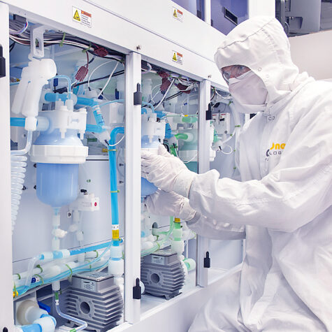
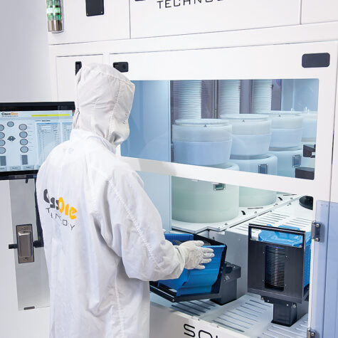
The G10-GaN by AIXTRON is a state-of-the-art deposition system for 150/200 mm GaN epitaxy, designed for GaN power and RF applications. It features a compact cluster design with three process chambers, reducing the footprint by 50% while maximizing wafer yield per square meter. This system significantly improves device yield with a threefold increase in on-wafer uniformity and maintains low particle levels, enhancing overall quality and consistency.
Cost-effectiveness is a key attribute, with the G10-GaN offering more than 25% lower epitaxial cost per wafer compared to other platforms. It incorporates Planetary Reactor® technology for high wafer yield and uniformity. The system's productivity is marked by over 90% equipment uptime and highest throughput per fab area, supported by features like fully automated wafer handling and advanced temperature control.
The G10-GaN ensures easy maintenance and operation with features like automated chamber cleaning and predictive functionalities. It's compatible with existing AIX G5+ C tools, facilitating seamless process transfers. Overall, the G10-GaN epitaxy system combines efficiency, cost-effectiveness, and advanced technology, making it an optimal choice for semiconductor manufacturing in the GaN sector.
Market opportunity for GaN for MOCVD and ALD
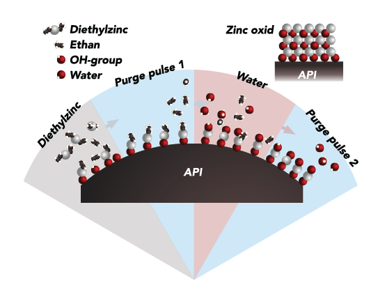
Tuesday, November 21, 2023
Revolutionizing Power Technology: Intel's Integrated CMOS Driver-GaN (DrGaN) Power Switch for Enhanced Efficiency and Density in Data Centers and Networks
Friday, November 17, 2023
Forge Nano Unveils Plans for U.S.-Based Lithium-Ion Battery Gigafactory in North Carolina, Set to Launch in 2026
Forge Nano, Inc. has announced its venture into lithium-ion battery manufacturing with the creation of Forge Battery. The company plans to establish a Gigafactory in Raleigh, North Carolina, targeting defense, aerospace, and specialty electric vehicle markets. With an initial investment of over $165M, the facility, operational by 2026, will produce batteries utilizing Forge Nano’s Atomic Armor surface technology, enhancing energy density, safety, and lifespan.
This technology is expected to surpass existing lithium-ion cells in performance. The North Carolina facility, benefiting from state incentives and a Job Development Investment Grant, promises significant economic benefits, including hundreds of high-paying jobs and substantial tax revenue to support local communities. The groundbreaking event is scheduled for the first half of 2024.
- Forge Nano has raised $81.54M over 10 rounds.
- Forge Nano's latest funding round was a Series C for on May 30, 2023.
Source:
Forge Nano Stock Price, Funding, Valuation, Revenue & Financial Statements (cbinsights.com)
Thursday, November 16, 2023
ALD is coming home 2024!
Announcement for the AVS 24th International Conference on Atomic Layer Deposition (ALD 2024) & 11th International Atomic Layer Etching Workshop (ALE 2024)
Event Overview: The AVS 24th International Conference on ALD along with the 11th International ALE Workshop will be held from August 4-7, 2024, at Messukeskus, Helsinki, Finland. This premier event, alternating annually among the United States, Europe, and Asia since 2001, focuses on the science and technology of atomic layer controlled deposition of thin films and atomic layer etching.
Special Celebration: The conference marks the 50th anniversary of ALD, celebrating the pioneering work of Dr. Tuomo Suntola, who filed the first patent on Atomic Layer Epitaxy in 1974. Dr. Suntola will open the conference with a special address.
Program and Submission Details: The event features pre-conference tutorials and a welcome reception on August 4, followed by sessions and an industry tradeshow from August 5-7. The program chairs include esteemed professionals from the University of Helsinki, the University of Twente, and AlixLabs AB. Key dates for abstract submission, registration, hotel reservations, and manuscript submissions are provided, with the abstract submission deadline being February 15, 2024.
Contact Information: Further details, including the event code of conduct, presentation guidelines, and sponsor and exhibitor information, are available for download. For any additional queries, Della Miller, the Event Manager, can be contacted at della@avs.org.
For more details, attendees and interested parties are encouraged to visit the official website of AVS.
Aixtron Reports Strong Revenue Growth and Doubled Profits in Q3 2023, Driven by High Demand for GaN and SiC Power Electronics
In Q3 2023, Aixtron SE, a deposition equipment maker based in Herzogenrath, Germany, reported a revenue of €165 million, marking an 86% increase from the previous year but a 4.9% decrease from the last quarter. The company's revenue for the first nine months of 2023 rose by 49% year-on-year to €415.7 million, predominantly from equipment sales.
A significant portion of the revenue came from the sale of metal-organic chemical vapor deposition (MOCVD)/chemical vapor deposition (CVD) systems for manufacturing gallium nitride (GaN) and silicon carbide (SiC) based power electronics, which accounted for 82% of equipment revenue. There was a notable shift from optoelectronics and LED systems to SiC and GaN-based systems.
Regionally, Asia contributed 44% of the revenue, followed by Europe (33%) and the Americas (23%). The gross margin improved to 46% in Q3 from 42% in Q2, with operating profit doubling year-on-year due to a better product mix.
However, the company faced increased operating expenses, primarily due to a 44% rise in R&D costs. This led to a significant drop in free cash flow, mainly attributed to a rise in inventories in anticipation of higher business volumes.
Aixtron launched the G10-GaN system, an addition to its G10 product line, which is expected to generate over 50% of its total GaN revenues in 2024. Despite a dip in order intake in Q3, Aixtron projects a higher intake in Q4 and confirms increased full-year growth guidance, expecting continued strong demand, especially for efficient power electronics.
The company is also investing in a new Innovation Center to expand its R&D capabilities, aligning with global trends in electrification, digitalization, and renewable energies, where materials like SiC and GaN are becoming mainstream.
Source:
Friday, November 10, 2023
ClassOne Technology Equips VTT Finland with Advanced Electrplating System for Chip Packaging Innovation"
Tuesday, November 7, 2023
Molybdenum: The New Frontier in Semiconductor Metallization according to Lam Research
Veeco Delivers Groundbreaking NSA500 Annealing System to Tier 1 Logic Customer
MSP Launches Turbo II™ Vaporizers: Next-Gen Efficiency for Semiconductor Fabrication
MSP, a Division of TSI, has introduced the Turbo II™ Vaporizers, transforming vapor delivery for chemical vapor deposition (CVD) and atomic layer deposition (ALD) in semiconductor manufacturing. These vaporizers handle a variety of liquid precursors, including thermally sensitive ones, and boast a 200% increase in vapor output with half the size of previous models. They offer higher vapor concentrations, quicker stabilization, and faster deposition times, reducing wafer processing time and liquid waste. Additionally, the vaporizers are designed to decrease downtime and maintenance, offering a lower total cost of ownership and significant long-term cost savings. MSP's product line includes various vaporizers, VPG filters, liquid flow controllers, and semiconductor metrology equipment.
Source:
Sunday, November 5, 2023
Global Semiconductor Sales See Mixed Trends: Monthly Rise Amid Annual Decline
Friday, November 3, 2023
Nanexa AB Concludes Rights Issue on Nasdaq First North Growth
Nanexa AB's rights issue, aimed at raising SEK 121m, concluded with a 34.7% subscription rate using rights and without. The company will utilize guarantee commitments for the remaining 27.1%. The rights issue, announced on September 21 with backing for 62% of the total, resulted in 33.5% of shares subscribed with rights and 1.2% without. The capital raised before transaction costs will be SEK 75m. Trading in BTAs will occur until registration is completed around week 45, 2023, with the new shares expected to trade on Nasdaq First North Growth by week 46, 2023.
Nanexa, founded in 2007, has evolved from working with Atomic Layer Deposition (ALD) technology for various applications to focusing on the pharmaceutical sector with its proprietary PharmaShell® system. PharmaShell® positions Nanexa in the burgeoning drug delivery market with a system that allows high-precision, long-acting injectable drug products. The company is developing its own products and also partners with multiple pharmaceutical firms, including AstraZeneca, leveraging the unique capabilities of its ALD-based technology to enhance drug delivery.
Dutch Election Frontrunner Advocates for Earlier ASML Export Restrictions to China
Dilan Yesilgoz-Zegerius, the leading candidate in the Dutch elections, has stated that the Netherlands should have responded more swiftly to restrict exports of ASML Holding NV's advanced chipmaking equipment to China. The U.S. has coordinated with the Netherlands and Japan to impose these export bans, which are set to take effect in January, in an effort to prevent China from using the technology to gain a military advantage. ASML, the most valuable Dutch company, has opposed these restrictions.
A recent incident where Chinese company Semiconductor Manufacturing International Corp. used ASML equipment to make advanced processors for Huawei smartphones underscores the urgency and the missed opportunity for earlier action by the Netherlands.
Yesilgoz-Zegerius acknowledged that the Netherlands had been "naive" about its security, emphasizing the need for cooperation with the U.S. to ensure independence from undesirable collaborations. Her stance, however, contrasts with some local lawmakers who criticize the export curbs as an infringement on Dutch sovereignty.
As she vies to become the Netherlands' first female prime minister and the first refugee to hold the position, Yesilgoz-Zegerius has made headlines with her tough stance on immigration, opposing a parliamentary motion that reduces tax benefits for expats and arguing for a significant reduction in migrant numbers. Her comments have sparked debate among Dutch tech companies like ASML, which rely on international expertise and have expressed concerns about the tightening of such tax benefits.
Source:
ASML China Export Curbs Too Late, Yesilgoz-Zegerius Says - Bloomberg
ALD Adaptation Promises Advances in Solid-State Battery Development
Entegris Reports Q3 2023 Revenue of $888M; Sees Rising Customer Interest in Innovative Solutions
Entegris, Inc. reported Q3 2023 revenue of $888 million, an 11% decrease YoY and 1% sequentially. GAAP net income was $33.2 million ($0.22 per share), including expenses like goodwill impairment and integration costs. Non-GAAP net income was $103.6 million ($0.68 per share). Q4 2023 sales are expected to be down around 2% sequentially, with GAAP EPS of $0.25-$0.30 and non-GAAP EPS of $0.55-$0.60. Customer interest is rising in Entegris' comprehensive solutions and collaborative materials development capabilities, particularly in materials like molybdenum. These solutions lead to faster development and speedier product launches, positioning Entegris as an innovation and growth partner.
Entegris, Inc. reported its third-quarter financial results for 2023, with revenue totaling $888 million, reflecting an 11% decrease compared to the same quarter in the previous year and a 1% sequential decrease. The company's GAAP net income for the third quarter was $33.2 million, resulting in earnings per diluted share of $0.22. These figures included various expenses, such as goodwill impairment, amortization of intangible assets, integration costs related to an acquisition, and other net costs. On a non-GAAP basis, the company achieved a net income of $103.6 million, with non-GAAP diluted earnings per share of $0.68.
For the fourth quarter of 2023, the company expects sales to be down approximately 2% sequentially, with a range of $770 million to $790 million in sales and diluted earnings per common share between $0.25 and $0.30 on a GAAP basis, while non-GAAP earnings per share are expected to range from $0.55 to $0.60.
Entegris operates in three segments: Materials Solutions (MS), Microcontamination Control (MC), and Advanced Materials Handling (AMH), catering to the semiconductor and high-tech industries. The company held a conference call to discuss its results on November 2, 2023.
Entegris is experiencing rising customer interest in their comprehensive solutions and collaborative capabilities for materials development, such as molybdenum. Customers appreciate the benefits, such as faster development and improved speed, resulting in quicker product launches. This positions Entegris as a valuable partner in their customers' innovation and growth endeavors.
Switching to molybdenum (Mo) in semiconductor manufacturing for 2 nm affects multiple processes. Mo offers conductivity without needing barrier layers and is cost-effective, but its corrosion risk requires adapting steps like deposition and etching. For chemical mechanical planarization (CMP), slurries and pads must be refined to protect Mo, with lower oxidizer concentrations and customized pad designs. Word line etching, particularly for 3D NAND, faces challenges with conventional etchants and cleans, necessitating specialized etchants that prevent residue. High-purity materials and rigorous filtration are essential for yield, with in situ monitoring and multiple-stage filtration to minimize contamination. Transitioning to Mo demands a comprehensive approach to select chemicals, pads, and filters to optimize the process and yield. Close collaboration with suppliers that provide integrated solutions can smooth the transition, as using a single supplier can expedite material compatibility testing and streamline the switch.
Source - Entegris.com
The memory market presents a mixed scenario. DRAM has shown anticipated improvement, but 3D NAND remains subdued, with declining wafer starts in Q3 and no significant recovery expected in Q4. These conditions align with previous industry forecasts. Looking ahead to 2024, specific details are not yet available, but there is an expectation of increased wafer starts. More precise information will be provided in the Q4 earnings report in February, as it's currently too early to offer comprehensive insights into the upcoming year's market dynamics.
In the current year, the company has observed that all node transitions in the logic sector have occurred according to schedule, which has had a positive impact on its business performance, notably in Taiwan during the third quarter. However, within the memory segment, the company had previously forecasted delays and a lack of transitions in 3D NAND, and these expectations have been met. The initial anticipation was for many customers to adopt 200-plus layer architectures by the year's end, but this transition has not materialized as predicted. The company is now looking forward to the possibility of high-volume production at 200 layers or more in early 2024, marking a revised timeline for this development.
Sources:
Entegris, Inc. (ENTG) Q3 2023 Earnings Call Transcript | Seeking Alpha
New Materials: Smoothing the Transition to Molybdenum (entegris.com)
Migrating to Molybdenum: Comprehensive IC Solutions to Streamline the Transition (entegris.com)
Thursday, November 2, 2023
Atlas Copco to Bolster Semiconductor Portfolio with Acquisition of South Korean Vacuum Valve Company, Presys Co., Ltd.
- Atlas Copco set to acquire South Korean vacuum valve producer, Presys Co., Ltd.
- Presys reported a revenue of MKRW 35,000 in 2022 and has a workforce of 134.
- The deal, pending regulatory approval, is anticipated to close in Q1 2024.
Wednesday, November 1, 2023
KTH and Green14 Innovates Green Silicon Production to Challenge Asia's Dominance in Solar Cell Market
The traditional methods dependent on fossil fuels to reduce silicon dioxide are being challenged by KTH and Green14's reactor, which has a fossil-free process using hydrogen-based plasma reduction. This high-temperature plasma, created from a combination of hydrogen and argon gas, emits water vapor instead of carbon dioxide and has silane as another byproduct, used for producing silicon anodes for lithium-ion batteries.
KTH (Royal Institute of Technology in Stockholm, Sweden) is challenging China's silicon production. A portrait depicts researcher Björn Glaser in a lab hall, pointing out the location where a reactor will be constructed. This seven-meter-tall reactor, being developed in collaboration with startup company Green14, aims to produce green silicon at KTH and challenge Asia's dominance in the solar cell silicon market.
Björn Glaser, researcher and project manager, points out the location in the so-called furnace hall where a reactor will be built. (Photo: Anna Gullers)
In a few months, the new reactor will begin construction at the Department of Materials Science, reaching the ceiling of the grand furnace hall, becoming KTH's largest pilot facility. The researchers aim to develop a process for silicon production that's faster and more environmentally friendly than previous methods.
Using 3,000-degree hydrogen plasma, the reactor will convert silicon dioxide to silicon, crucial for manufacturing solar cells and semiconductors. Unlike traditional methods that rely on fossil fuels, this process with hydrogen plasma emits water vapor instead of carbon dioxide.
The primary goal is to produce silicon suitable for solar cells, a market dominated by Asia, particularly China. Björn Glaser, a lecturer and expert in high-temperature metallurgical experiments, believes this could be a game-changer, potentially bringing Europe back into competition.
Green14, the startup behind the initiative, will own and operate the facility, with Björn Glaser and Adam Podgorski, an Australian chemist and CEO of Green14, working closely together. If successful, Green14 plans to build a larger facility in northern Sweden. However, a significant challenge is ensuring safety due to the combination of extremely high temperatures and hydrogen gas.
Björn Glaser expresses that the project not only provides good PR for KTH but also offers students a unique opportunity to engage in groundbreaking research. If successful, the process could revolutionize how other metals, like copper, titanium, and vanadium, are produced, reducing their carbon footprints and making them cheaper to manufacture.
About GREEN14
GREEN14 is a pioneering technology company committed to developing innovative solutions for a sustainable future. With a focus on renewable energy, GREEN14 is revolutionizing the production of solar grade silicon through its groundbreaking quartz reduction process. By combining cutting-edge technology with a commitment to environmental stewardship, GREEN14 is driving the transition to a low-carbon economy and paving the way for a cleaner, brighter future.
Sources:
Surge in HBM Demand Marks Memory Market Recovery and Anticipated Growth in 2024 for Samsung
Samsung Electronics' financial results for 3Q23 highlighted a 12% QoQ revenue increase to 67.40 trillion Korean won, although there was a 12% YoY decrease. Notably, the company reported its highest quarterly profit for the year. Despite potential economic uncertainties in 2024, Samsung is optimistic about the recovery of the memory market and the rebound in smartphone demand.
The memory sector saw a recovery compared to the previous quarter, especially in PC and mobile due to the rise in adoption of high-density DRAM and NAND products. The completion of customer inventory adjustments also played a role. Server demand was subdued for traditional servers due to macroeconomic uncertainties. However, strong demand persisted for AI-oriented high-density products. Samsung emphasized its focus on expanding sales of advanced node products like HBM DDR5, LPDDR5, and UFS 4.0. They also intend to manage high inventory products through production adjustments. The company expects the recovery trend in the memory market to accelerate further in the fourth quarter. Additionally, there has been a notable surge in HBM demand and the company is actively advancing its HBM businesses and plans to augment its HBM supply capacity by 2.5 times next year.
Trendforce on X (LINK)
The foundry division secured a record number of new orders, particularly in the HPC domain, despite a slow recovery in the mobile market. The new Taylor factory in Texas is set to begin production using the second-gen 3nm GAA process. The advanced packaging business has also been flourishing with orders from both domestic and international HPC clients.
Profits in the mobile panel business surged due to new flagship models from major clients. In contrast, the large panel business faced tepid demand. Samsung aims to cater to the growing mobile panel demand and increase profitability in the large panel sector by introducing new products and enhancing yield rates.
With the global economy expected to bounce back in 2024, the smartphone market's demand is anticipated to surge. High-end market growth is likely to continue, driven by the global recovery of the smartphone market.
Looking ahead to 2024, Samsung anticipates increased PC and mobile demand due to product replacement cycles initiated during the pandemic's early phase. High-density trends in both DRAM and NAND are expected to persist, propelled by on-device AI advancements. The company plans to focus on advanced node products, including 1B nanometer DDR5, LPDR5X, PCI Gen 5, and UFS 4.0, to bolster product competitiveness and profitability. Emphasizing the growing demand for generative AI, Samsung aims to strengthen its market position with high-density, low-power, and high-performance products for on-device AI, which has recently gained significant attention.
Sources;
Samsung Electronics Co Ltd (SSNLF) Q3 2023 Earnings Conference Call Transcript | Seeking Alpha
Tuesday, October 31, 2023
Micron's Distinct Approach to DRAM and Apple Design Wins
The tech landscape has seen consistent advancements, especially with the D1β (D1b) DRAM generation. Micron's D1β LPDDR5 16 Gb DRAM chips, integrated into the Apple iPhone 15 Pro, represent a significant step forward. Codenamed Y52P die, this chip offers an improved form factor and density, especially when contrasted with its LPDDR5/5X D1α 16 Gb predecessor. The integration of these chips into Apple's flagship device marks a significant design win for Micron, emphasizing the trust and partnership between the two tech giants.
In a recent teardown of the Apple iPhone 15 Pro, TechInsights has discovered a remarkable find - Micron's cutting-edge D1β LPDDR5 DRAM chips. These chips mark the industry's first foray into the D1β generation, and they are nothing short of impressive. (LINK)
Micron's technological direction is unique, especially with their decision to forego the Extreme Ultraviolet Lithography (EUVL) process, common in sub-15nm DRAM scaling. This stands in contrast to industry giants like Samsung and SK Hynix, who employ EUVL in their DRAM fabrication. Despite this, Micron has successfully launched the D1z, D1α, and D1β DRAM chips without EUVL, illustrating an alternative yet effective DRAM scaling approach.
In wrapping up, while Samsung and SK Hynix utilize EUVL in their DRAM processes, Micron has carved a different path, further solidified by their design wins with Apple. This partnership not only underscores Micron's technological prowess but also indicates the potential of varied methodologies in shaping the future of DRAM technology.
Canon's Nanoimprint Leap: Challenging ASML's Dominance in Semiconductor Lithography
According to Lithography expert Dr. Frederick Chen, Canon's statement on nanoimprint technology status following mid-October announcement indicated they were still facing challenges before reaching the levels required for mass production.
Canon's statement on nanoimprint technology status following mid-October announcement indicated they were still facing challenges before reaching the levels required for mass production. https://t.co/Z58su0Mkje
— Fred Chen (@DrFrederickChen) October 30, 2023
Thursday, October 26, 2023
Kokusai Electric's Stellar Tokyo IPO: A Surge in Stock, High Hopes for the Future
Kokusai Electric's stock rose 28% in its Tokyo debut after KKR sold its shares for $724 million, marking Japan's largest IPO in five years. Closing at 2,350 yen, Kokusai's valuation reached $3.61 billion. This was the biggest Tokyo listing since SoftBank Corp. in 2018. KKR reduced its stake from 73.2% to 47.7%. Analysts noted a challenging market for chip-related stocks but anticipate a rebound for Kokusai. The company specializes in machines for silicon wafer films, with major clients like Samsung. Despite a predicted profit drop, Kokusai's President sees growth potential by 2025. KKR's previous sale attempt to Applied Materials was unsuccessful. The IPO saw huge interest, with foreign investors oversubscribing by over 10 times.
Source: Kokusai Electric shares jump 28% in Tokyo debut - Nikkei Asia
Wednesday, October 25, 2023
Infineon Acquires GaN Systems for $830M, Bolstering Position in Power Semiconductor Market
Strategic Move Amplifies Infineon's GaN Expertise, Accelerating Energy-Efficient Solutions and Decarbonization Efforts
Infineon Technologies has successfully acquired GaN Systems, a Canadian company, for $830 million. This acquisition positions Infineon as a significant supplier of gallium nitride (GaN) power devices across various sectors, including consumer, industrial, and automotive applications. With the deal, Infineon inherits a wide array of GaN-based power conversion devices, designs, and advanced application expertise. GaN Systems, located in Ottawa, has integrated with Infineon, which already had its CoolGaN range. Jochen Hanebeck, Infineon's CEO, emphasized that GaN technology promotes energy efficiency and contributes to decarbonization efforts. Following this acquisition, Infineon boasts 450 GaN experts and access to over 350 GaN patent families, solidifying its leadership in the power semiconductor domain. The collaboration of both companies' intellectual properties, application insights, and customer projects optimally positions Infineon for future growth.
Notably, GaN Systems has a unique island-based device structure that enhances power design performance, utilized by companies like QPT for fast switching speeds of up to 20MHz. This acquisition comes after Infineon's 2020 purchase of Cypress Semiconductor.
Source: Infineon completes acquisition of GaN Systems ... (eenewseurope.com)
Monday, October 23, 2023
TSMC To Report Breakthrough in NMOS Nanosheets Using Ultra-Thin MoS2 Channels at IEDM 2023
Sunday, October 22, 2023
Hamas' Brutal Attacks on Israel Could Disrupt Global Tech Supply Chain and Intel's Expansion Plans
China Tightens Grip on Vital Graphite Exports Amid Global EV Surge: Implications for U.S. Battery Industry and Beyond
From December 1, China will mandate export permits for certain graphite products to safeguard national security amidst increasing international scrutiny over its manufacturing dominance. China supplies 67% of global natural graphite and refines over 90% used in EV battery anodes. This move coincides with foreign governments pressuring Chinese firms on their industrial practices. The U.S. and European Union are implementing measures against Chinese products and technologies. New Western investments aim to counter China's graphite dominance, but success remains uncertain.
According to the USGS, in 2022, the United States did not produce any natural graphite. Instead, 95 U.S. companies consumed 72,000 tons of it, valued at $140 million. These companies were mainly located in the Great Lakes and Northeast regions. Natural graphite was used in batteries, brake linings, lubricants, steelmaking, and other applications. The U.S. imported an estimated 82,000 tons of graphite in 2022, with 77% being flake and high-purity graphite. Due to the rising electric-vehicle market, graphite consumption is expected to grow. Since 2018, the global battery market for graphite has surged by 250%. The U.S. has four operational lithium-ion battery plants and 21 more in development. These plants, when fully operational, will need about 1.2 million tons of spherical purified graphite annually, with 40%-60% sourced from synthetic graphite.
U.S. graphite imports saw a decline in 2019 and 2020 but rose by 55% in 2022. This increase is attributed to the demand from the lithium-ion battery industry. China dominated the graphite production in 2022, accounting for 65% of the global output. North America's graphite production was just 1.2% of the global supply. Projects to explore and produce graphite are ongoing worldwide. The geopolitical conflict in Ukraine has impacted graphite production and trade relations, affecting the global graphite market.
Europe heavily relies on graphite imports, primarily from China, but aims to reduce this dependency by advancing local mining projects. The EU has categorized graphite as a critical raw material due to its importance in the EV battery sector. Notably, mining initiatives in Sweden, such as Woxna Graphite Mine, and Norway's Skaland Graphite operation are underway to bolster local supply chains. With the rise of European battery gigafactories, securing a stable graphite supply has become imperative.
Why is graphite important?
Graphite is a crucial component in electric vehicle (EV) batteries, specifically in the lithium-ion batteries that power most EVs. Here's how graphite is used:
Anode Material: In a lithium-ion battery, there are three primary parts: the cathode (positive electrode), the anode (negative electrode), and the electrolyte. Graphite is used as the primary material for the anode. When the battery is being charged, lithium ions move from the cathode through the electrolyte and get stored between the layers of graphite in the anode.
Conductivity: Graphite is a good conductor of electricity. This property is essential for efficiently moving electrons in and out of the anode during the charging and discharging cycles of the battery.
Stability: Graphite has a layered, planar structure. This allows lithium ions to easily slip between these layers, a process called intercalation. This structure provides a stable housing for lithium ions, ensuring the battery's longevity and safety.
Volume Expansion: One of the challenges with lithium-ion batteries is that materials can expand and contract significantly as they absorb and release lithium ions. Graphite's structure can accommodate this volume change, helping to maintain the integrity of the electrode.
Natural vs. Synthetic Graphite: There are two main types of graphite used in EV batteries: natural flake graphite and synthetic graphite. Both types can be processed to achieve the desired properties for battery anodes. While natural graphite is mined, synthetic graphite is produced from petroleum coke.
The increasing demand for EVs has led to a surge in the need for graphite. As a result, the sourcing, processing, and supply chain for graphite have become critical considerations for the battery and EV industries.
Sources:
China, top graphite producer, to curb exports of key battery material (cnbc.com)