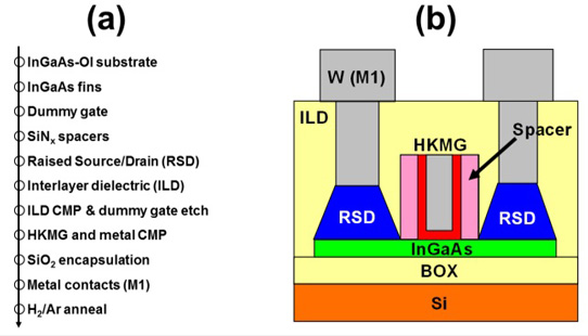
Friday, January 29, 2016

HERALD Novel High-k Workshop Call for abstracts until Jan 31, 2016 - Working Group 4 Event

Reminder: Call for abstracts until Jan 31, 2016 - Working Group 4 Event

In collaboration with the EU COST networking project HERALD, NaMLab invites to the ‘Novel High-k Application Workshop’ on March 14th and 15th, 2016. New challenges offered by the application of high-k dielectric materials in micro– and nanoelectronics will be discussed by more than 80 participants from industry, research institutes and universities. The workshop was initiated as a stimulating European platform for application-oriented scientists to exchange ideas and discuss latest experimental results on MIM-capacitors, process technologies, leakage & reliability as well as characterization of high-k dielectrics integrated in silicon based micro– and nanoelectronics. In addition, new results in the field of ALD dielectrics in solar cells, transparent conduction oxides (TCOs) and atomic layer etching (ALE) will be discussed.

A long list of speakers already confirmed their participation at the workshop. A preliminary program can be found here: http://www.namlab.com/news/events-1/novel-high-k-application-workshop.

To participate in the workshop, please apply by the end of January 2016 with a ½ page abstract (oral or poster) describing the work you would like to present. Mail your abstract to ALD@namlab.com

Since the HERALD project aims to promote participation from new EU member countries, additional travel grants (up to €300 per person) are available. If you would like to apply for a travel grant, please state this in your email.

COST Action MP1402 - HERALD
Hooking together European research in Atomic Layer Deposition


Wednesday, January 27, 2016

IBM Research present InGaAs on insulator FinFET process using Plasma Enhanced ALD HKMG

IBM Research GmbH in Switzerland has developed an n-channel indium gallium arsenide (InGaAs) on insulator fin field-effect transistor (FinFET) process and claims the highest on-current to date for CMOS-compatible InGaAs devices integrated on silicon (Si) [Vladimir Djara et al, IEEE Electron Device Letters, published online 1 January 2016].

According to the paper, the devices were fabricated using a replacement metal gate (RMG) flow, including ultra-thin SiN spacers, scaled high-k/metal gate (HKMG), and highly-doped raised source and drain (RSD) modules for improved electrical performance.

ALD Inside:
  • 12-nm-thick SiN spacers were deposited by plasma-enhanced atomic layer deposition (PEALD)
  • After dummy gate removal, a HKMG, featuring a scaled Al2O3/HfO2 dielectric stack with a capacitance equivalent thickness (CET) of ∼1.5 nm, was deposited using a highly conformal and uniform PEALD process. the process has previously been published here.  The tool used is a FlexAL ALD from Oxford Instruments and the PEALD processes are TMA and O2 plasma for Al2O3 and TEMAH and O2 plasma for HfO2.
The FlexAL® systems provide a new range of flexibility and capability in the engineering of nanoscale structures and devices by offering remote plasma atomic layer deposition (ALD) processes and thermal ALD within a single ALD system.

Pretty cool if you ask me to see that PEALD is used for gate dielectric, which is usually not the case on silicon channels where thermal HfCl4/H2O process is dominating and also that TEMAHf can perform this good as a gate dielectric. Please read the full report in Semiconductor Today here.

Trending ALD News January 2016

Tuesday, January 26, 2016

ALD sales booming for Arradiance GEMStar XT line

It seems that the rather wicked prognosis made by Gartner and others that ALD equipment market will doouble until 2018 may really be for all and not only the semiconductor OEMs. Here is goood news froom Arradiance that are steaming away!


As announced by Arradiance: Sales of GEMStar XT benchtop ALD systems including rapid market adoption of the new GEMStar XT-P plasma-enhanced system resulted in 73% sales growth in 2015 Coupled with a strengthened balance sheet, Arradiance expects to outgrow the market again in 2016.

GEMStar-8 XT PEALD™ Benchtop PEALD/Thermal ALD System


Arradiance LLC, manufacturer of the popular GEMStar family of benchtop Atomic Layer Deposition (ALD) systems for research and light production, today announced an impressive 73% sales growth for 2015 of their highly popular GEMStar family of benchtop Atomic Layer Deposition (ALD) systems for research and light production. 

“We are extremely gratified by the market acceptance of our GEMStar XT line of thermal ALD systems. Most notable is the adoption of our new GEMStar XT-P plasma plus thermal system; the world’s only commercial benchtop, plasma-enhanced tool,” said Arradiance President, Ken Stenton. 

The reactors are stackable!


“Introduction of plasma capability to our benchtop architecture has raised the profile of the product line to a new level,” explained Mr. Stenton. “Customers now view Arradiance as a full-service ALD equipment company, on par with or exceeding the capabilities of companies that offer much larger and more expensive commercial systems. The number of films and applications being developed on the GEMStar systems is growing geometrically.”

Arradiance entered the ALD equipment market in 2010 and has since become one of the fastest growing companies in a crowded field. Customers cite innovation, attention to design detail and superior aftermarket service as some of the reasons for the company’s growing success. Looking forward, Mr. Stenton predicted that, “Coupled with an increased level of support from our investment partners, our existing backlog and sales pipeline should propel Arradiance sales growth to again outpace the market in 2016. Driven by new applications in energy, bio-engineering and high energy physics, demand for reasonably priced, full feature ALD systems continues to grow.”

UPDATE: Jusung Engineering launches SDP R2 Revolution-Rotation ALD System at SEMICON Korea

JUSUNG Engineering Co., Ltd., incorporated founded in 1995, is one of the leading equipment makers in global semiconductor, flat panel display and solar cell markets from South Korea. Today at SEMICON Korea Jusung announced a new cool ALD platform (Press release, Korean) and in English below (supplied by Jusung Engineering).


SDP R2(Revolution/Rotation Atomic Layer Deposition System), featuring entirely new concept chamber to realize high-quality film even at an ultra-low temperature (Picture from Jusung Engineering Korean Press release).


JUSUNG Engineering (Ticker 036930; CEO Chul Joo Hwang) will participate in the SEMICON Korea 2016, an international semiconductor equipment and material expo held in the Coex for three days starting from January 27th 2016 to showcase its next-generation semiconductor equipment.

JUSUNG plans to launch its state-of-the-art products including SDP R2(Revolution/Rotation Atomic Layer Deposition System), featuring entirely new concept chamber to realize high-quality film even at an ultra-low temperature.


 The SDP R2 is new concept equipment that enables revolution for the main disc and rotation for the water simultaneously in order to fulfill the demanding technical requirement in the multi-patterning process at the tech-migration which is at the verification test stage on the mass- production line of a customer.

The equipment allows film quality deposition without using plasma even at an ultra low temperature below 80℃, causing no damage to film quality at infrastructure, and enables the plasma function at the treatment process, realizing the merits of both thermal deposition and plasma deposition processes at the same time. Above all, the most notable feature of the equipment is the ability to control the uniformity of the deposition material in a 20nm or smaller micro semiconductor structure through revolution and rotation function, ensuring excellent film quality without regard to the complexity of the infrastructure.

Once the new concept technology is applied to mass-production, the application will be widely extended to processes such as next-generation memory semiconductor, DRAM and Flash thanks to improved semiconductor film quality profile along with reduced time requirement for deposition, leading to higher productivity as well as lower cost.

An officer from JUSUNG Engineering said, “We showcase new concept equipment that is optimized to the tech migration process at an event where you can see the recent technology trends in the semiconductor industry at a glance…We will do our utmost to keep our technology well ahead in the industry with new product development to overcome limitations of existing equipment for next-generation semiconductors.”

Picosun sees growth for their clustered ALD Batch Product line in the growing MEMS industry


Earlier this year this blog reported on expected growth for ALD OEMs due to capital investments driven by 14 & 10 nm at TSMC and other Foundries - 2016 will be a good year for the ALD Equipment Manaufacturers. Another area that is rapidly introducing ALD processes is MEMS. Finnish ALD Company Picosun is experiencing revenue from the MEMS Industry and sees a big future growth opportunity in this area, having a competitive edge by their batch ALD cluster tools.

In 2014, the MEMS sector represented an $11.1B business for Si-based devices according to Yole Développement (Yole) latest MEMS report “Status of the MEMS Industry”.

According to Yole, the MEMS industry is forecasted to exceed $20B by 2020 and lead by the “MEMS Titan” Robert Bosch (Bosch). Picosun and Bosch  has a collaboration in ALD as announced in 2014 (http://www.picosun.com/sitenews/view/-/nid/117/ngid/4). So it indeed seems that Picosun is very well positioned to take on a lead as a Tier1 ALD MEMS supplier.


Passivation of MEMS by Atomic Layer Deposition, Matthias Schwille, Robert Bosch (ALD Lab Dresden Symposium, SEMICON Europa 2015)

Under this new analysis entitled, “Status of the MEMS Industry” report Yole proposes a deep understanding of the MEMS markets trends and players dynamics. The More than Moore market research and strategy consulting company announces its 2014 MEMS manufacturers and foundries ranking and proposes an overview of the future game-changers including new devices, disruptive technologies, 300mm wafers, sensor fusion and new markets.


As reported by Picosun: Picosun Oy, the leading supplier of high quality ALD (Atomic Layer Deposition) thin film coating solutions for industrial production, has revolutionized cost-effective MEMS manufacturing with high throughput PICOPLATFORM™ batch ALD cluster technology.


MEMS (MicroElectroMechanical Systems; Microsystems) are micrometer-scale, semiconductor-based components that combine e.g. electrical, mechanical, and optical functions. They are present in our everyday electronics in products such as hard disk read heads, inkjet printer nozzles, microphone and videoprojector chips, and airbag controls, tire pressure monitoring, and driving stability systems in cars.

Fast, fully automated and economically feasible batch processing without compromising the strictest process quality and purity requirements of the semiconductor industries is the prerequisite for industrial breakthrough of the next generation MEMS devices. They realize improved data storage, mobile phone, GPS positioning, and automotive control electronics, and health care applications such as body area sensors and remote monitoring devices. Combining batch ALD processing with fully automatic, robotized PICOPLATFORM™ vacuum cluster systems enables super-fast throughput of MEMS chips with excellent yield, process purity and uniformity levels(*). 


Team Picosun

“Our MEMS customers gain immense benefits from our SEMI S2 certified PICOPLATFORM™ cluster technology. Equipped with our production-proven PICOSUN™ P-series batch ALD tools, these cluster systems have already proven their worth at the manufacturing sites of leading, global microsystems industries. Considering the MEMS market growth forecasts, propelled by the coming era of the Internet-of-Things, this product line will definitely be one of the cornerstones of our industrial ALD business,” states Mr. Timo Malinen, Chief Operating Officer of Picosun.

(*) Within-wafer, wafer-to-wafer, and batch-to-batch film thickness non-uniformity values (1σ) measured with 50 nm Al2O3 process on 200 mm Si wafers (25 wafers/batch) < 1%. The development work for batch ALD cluster technology has been performed in the project Lab4MEMS (1.1.2013 - 31.12.2015), coordinated by ST Microelectronics.

The project Lab4MEMS has received funding from the EC under the ENIAC Nanoelectronics Framework Programme (ENIAC-2012-2) under grant agreement no 325622-2.


Sunday, January 24, 2016

Strem Chemicals & Gordon Lab at Harvard collaborating on ALD Precursors


According to a recent press release (below) Strem Chemicals inc. in the US is now collaborating with the famous Gordon Research Group at Harvard on transition metal amidinate ALD Precursors. This collaboration includes the distribution of those precursors out of The UK and Ireland. Earlier the distribution here in Europe was through DOW but as previously reported DOW has dropped ALD precursors - so this is very good news for us here in Europe that Strem who has excellent distribution services will handle of this business here. Luckily I just got the new catalog from Strem and could look up some of these precursors including in the deal between Strem and Harvard (see pictures below).


Families of volatile metal available for use in ALD applications

Strem Chemicals Inc in the US works with Roy Gordon’s Group at Harvard University, who produce transition metal amidinates for metal, nitride and oxide layer deposition, allowing Strem Chemicals UK to distribute them in the UK and Eire.
Atomic Layer Deposition (ALD) is a vapour phase technique capable of producing thin films of a variety of materials.  As device requirements push toward smaller and more spatially demanding structures, ALD has demonstrated potential advantages over alternative deposition methods.  ALD offers exceptional conformity on high-aspect ratio structures, thickness control at the angstrom level, and tunable film composition from metal oxides to noble metals.  ALD has emerged as a powerful tool for many industrial and research applications including ferroelectric memories, switches, radiation detectors, thin-film capacitors and microelectromechanical structures (MEMS).  They also are affording significant improvements in solar cell devices, high-k transistors, solid oxide fuels, protective coatings, fuel cells, + ion- batteries and nanogratings. 

Saturday, January 23, 2016

Lam Research is taking a lead in Atomic Layer Etching (ALE)

Lam Research is taking a lead in Atomic Layer Etching (ALE) and is moving on fast introducing leading etch processing equipment for the advanced nodes.


 Lam Research reports in a recent article in Semiconductor Engineering (here): 

Atomic layer etching (ALE) is a technique for removing thin layers of material using sequential reaction steps that are self-limiting. ALE has been studied in the laboratory for more than 25 years. Today, it is being driven by the semiconductor industry as an alternative to continuous etching and is viewed as an essential counterpart to atomic layer deposition. As we enter the era of atomic-scale dimensions, there is need to unify the ALE field through increased effectiveness of collaboration between academia and industry, and to help enable the transition from lab to fab. With this in mind, this article provides defining criteria for ALE, along with clarification of some of the terminology and assumptions of this field. To increase understanding of the process, the mechanistic understanding is described for the silicon ALE case study, including the advantages of plasma-assisted processing. 


ALE Review by Keren Kanarik et al "Overview of atomic layer etching in the semiconductor industry" J. Vac. Sci. Technol. A 33, 020802 (2015); http://dx.doi.org/10.1116/1.4913379

A historical overview spanning more than 25 years is provided for silicon, as well as ALE studies on oxides, III–V compounds, and other materials. Together, these processes encompass a variety of implementations, all following the same ALE principles. While the focus is on directional etching, isotropic ALE is also included. As part of this review, the authors also address the role of power pulsing as a predecessor to ALE and examine the outlook of ALE in the manufacturing of advanced semiconductor devices.

For those of you that have missed the fantastic animation by Lam explaining ALE - here it comes again.

 
To learn more about ALE you should consider going to Dublin this summer for the ALD 2016 Conference which is also hosing the AVS ALE 2016 Workshop!


Hurry up ALD & ALE People - These articles on Atomic Layer Processing have been made free to download for a limited time!

Hurry up ALD & ALE People - These articles on Atomic Layer Processing have been made free to download for a limited time!


Journal of Vacuum Science & Technology A - 
First 2016 Issue Online Special Issue on ALD/ALE
2.322 
Impact Factor


Gartner says that 7nm will be delayed and 5nm will be pushed out ot 2023

10 nm FinFET may start to ship as early as end of 2016. However, according to a recent article by Mark Lapedus (at Semiconductor Engineering) Bob Johnson, an analyst at Gartner, projects that 7nm could get pushed out to 2020. "This, in turn, could impact the potential timing of 5nm, if the industry decides to move forward with the technology. “I assume 5nm will happen, but not by 2020,” Johnson said, adding that a viable 5nm process may not appear until the next decade, possibly 2023."

The slow down in scaling is not something new and has been seen for some time now. Above is a forecast presented at 2014 Semicon West with conclusions of the SEMI’s World Fab Forecast - Technology Node Transitions Slowing Below 32 nm. Her you can clearly see that the node transitions has paced slower since 28/32 nm.  The question now is then if the pace will come to a halt.

The current 3 main options for 5nm logic FETs are :
  • Gate-All-Around FETs based on III/V Nanowires
  • To extend FinFET
  • Monolithic 3D and other 2.5D/3D IC technologies

AVS ALE 2016 - Call for Papers, Dublin, July 24-25th

ALE 2016 - Call for Papers!

In conjunction with ALD 2016 in Dublin, Ireland, the AVS Plasma Science and Technology and Thin Film Divisions will be hosting the 3rd workshop on Atomic Layer Etching. 

Deadline: March 18, 2016 : http://ald2016.com/atomic-layer-etching-workshop-overview/


Plenary Speaker

•Ankur Agarwal (Applied Materials)

Invited Speakers
• Steven George, University of Colorado, Boulder
• Dennis van Dorp, IMEC
• Akira Koshiishi, Tokyo Electron
• Kazunori Shinoda, Hitachi Hi-Tech

ALE 2016 Workshop Overview

Extending Moore's law beyond the 10 nm node will increasingly rely on high precision processes employing new materials with high-quality surfaces. Atomic layer etching & atomic layer clean technology is a promising pathway to achieve these fundamental requirements.

In conjunction with ALD 2016 in Dublin, Ireland, the AVS Plasma Science and Technology and Thin Film Divisions will be hosting the 3rd workshop on Atomic Layer Etching. The 2nd ALE workshop was held in 2015, and attracted global participation, with nearly 280 attendees representing both academia and industry. The goals of the meeting are to provide research focus, report progress to-date, and foster collaboration to accelerate this unique capability. Latest findings are expected from experts at major universities, semiconductor manufacturers, and leading equipment suppliers. A broad range of topics are expected, including but not limited to:

• Surface chemical reactions
• Ion energy distributions and control
• Damage-free processes
• Modeling of processes and discharges
• Chemistry synthesis for 'reverse ALD'
• Interesting and new applications for ALE

Workshop Chairs

Bert Ellingboe, Dublin City University (albert.ellingboe@dcu.ie)

Sumit Agarwal, Colorado School of Mines (sagarwal@mines.edu) 


Friday, January 22, 2016

2016 Critical Materials Council (CMC) Seminar – Call for Papers

The Critical Materials Council (CMC) and TECHCET have issued a call for papers to be presented at the “Critical Materials for Device Driven Scaling” Seminar to be held May 5-6, 2016 in Hillsboro, Oregon, USA. Semiconductor manufacturing industry experts from IDMs, OEMS, and materials suppliers will gather to discuss actionable information on critical materials used in HVM fabs, while also looking at issues associated with new materials needed for future devices. Tim G. Hendry, Vice President, Technology & Manufacturing and Group Director of Fab Materials, Intel Corp., will provide the keynote address.


Following the annual members-only CMC meeting to be held May 3-4, the 2016 CMC Seminar is open to the public. Business drives our world, but technology enables the profitable business of manufacturing new devices in IC fabs, and new devices need new materials. In addition to panel discussions, presentation sessions will focus on the following topics:

I. Semiconductor Market Briefing: application-specific demands for devices and materials
II. Tracking the Supply Chain down to Earth, Wind, and Fire: manufacturing and supply chain
III. Emerging Materials Evolutions: alternate logic channels and new memory switches, and
IV. Materials Revolutions: beyond silicon CMOS.

Attendees will include industry experts handling supply-chains, business-development, R&D, and product management, as well as academics and analysts. The early-bird registration fee (before March 15th) for the CMC Seminar is $349; the standard registration fee is $425 (after March 15th). CMC member companies will be attending this meeting, as it is an important part of their membership. Additional information can be found online at http://cmcfabs.org/seminars.

To submit a paper for consideration, please send a 1-page abstract focusing on critical materials supply dynamics by February 29, 2016 to cmcinfo@techcet.com.

The Critical Materials Council for Semiconductor Device Fabricators was originally started by SEMATECH in the early 1990’s, and is now managed by TECHCET. It actively works to identify issues surrounding the supply, availability, accessibility, or lack thereof, of semiconductor process materials, current and emerging, also known as “Critical Materials”. This is done by collectively working to solve common materials related issues in a non-competitive environment. The CMC supports the continuous improvement of the Materials Supply Chain Community for Semiconductor Fabricators. For more information see www.CMCFabs.org .


Thursday, January 21, 2016

AVS - Atomic Layer Etching Workshop 2016, 24th-25th July 2016, Dublin, Ireland

Extending Moore’s law beyond the 10nm node will increasingly rely on high precision processes employing new materials with high-quality surfaces. Atomic layer etching & atomic layer clean technology is a promising pathway to achieve these fundamental requirements.


In conjunction with ALD 2016 the AVS Plasma Science and Technology Division will be hosting a workshop on Atomic Layer Etching.  The goals of the meeting are to provide research focus, report progress to-date and foster collaboration to accelerate this unique capability. Latest findings are expected from experts at major universities, semiconductor manufacturers and leading equipment suppliers.

Details regarding the workshop programme will be announced soon.

You can register for ALD2016 (one day or three days, 25-27 July) and the Atomic Layer Etch workshop (one day, 25 July), as well as for the joint ALD/ALE tutorial (half-day, 24 July). As part of the registration process and for tracking purposes, we ask that you indicate your primary interest in Atomic Layer Deposition or Atomic Layer Etching.

Register here.

Wednesday, January 20, 2016

Ferrotec and JSW AFTY Sign Joint Representation Alliance

Just when I thought that I had them all in my list another ALD company appears to me. Here is a highly interesting Japanese company JSW AFTY, that manufacture CCP ALD tools and also a magical ALD-ECR combination tool - ECR as in Electron Cyclotron Plasma. Check out their press release below on their new joint distribution with US company Ferrotec.


Ferrotec Corporation (JASDAQ: 6890) today announces a joint representation alliance between Ferrotec and JSW AFTY. With this alliance, JSW AFTY will represent Ferrotec's Temescal electron beam evaporators in the Japanese market, and Ferrotec will represent JSW AFTY's systems in the United States. The agreement spans sales, service and support and is expected to provide customers in both markets with an expanded local infrastructure.

With more than 1500 Temescal evaporation systems and over 16,000 E-beam guns and power supplies installed worldwide, Ferrotec's Temescal systems are the leading electron beam evaporators for global compound semiconductor Independent Device Manufacturers (IDMs) and foundries.

JSW AFTY's products include a unique line of Electron Cyclotron Resonance (ECR) Plasma and Atomic Layer Deposition (ALD) systems as well as their Hybrid ALD – ECR Deposition systems.

"We are pleased to be able to partner with the JSW AFTY team to help bring their unique high quality, low temperature and low damage deposition technologies to the US market. JSW AFTY's technology is increasingly important in the production of high power semiconductor laser, MR (MagnetoResistance) head and SAW devices," said Gregg Wallace, Managing Director of Temescal products at Ferrotec "We look forward to this partnership and the opportunity to introduce JSW AFTY's products to both our existing and new customers in USA."

"Ferrotec's Temescal electron beam evaporators have been tremendously adopted in compound semiconductor business field worldwide. By adding their product to our product lineup, we are now able to offer wider range of solutions to our Japanese customers," said Nobuhisa Kobayashi, President of JSW AFTY. "I'm certain that this alliance enables both companies to offer more flexible and perfect services to our customers by using each know-how as well as aftersales service network which have been accumulated for many years."

Tuesday, January 19, 2016

A Non-FinFET Path to 10nm Globalfoundries’ FD-SOI Alternative

STMicroelectronics and CEA/Leti have been leading an effort in scaling FD-SOI for long now and have recently gotten some muscles in support by fabing it at Samsung (28nm) and Globalfoundries Fab1 in Dresden (22nm). I ran some sub 22 nm development LOTs for one of our customers some years ago and form an ALD high-k point of view this was a a piece of cake. I gave them the same recipe, adjusted the thickness slightly, as the other guys and they didn't complain. That is why I since then always follow news on FD-SOI - it´s such an underdog technology compared to bulk FinFET in terms of ecosystem support and investments but I like underdogs - or  maybe rather medium sized dogs with a big dog attitude. Anyhow here is a recent feature article by GloFo on the topic that is worth reading:

It was the coolest transistor development in many a year. Rather than continually squishing transistor parts closer and closer together, we flipped it to vertical and celebrated the arrival of the FinFET.


Image courtesy GlobalFoundries

Which was great: it gave us a way to keep increasing performance in many of the applications where the value lies in the speed of the circuit. But after the initial party was over and we started picking up the pointy party hats and nursing the hangovers with massive doses of ibuprofen, we started looking at the bill. FinFET is nice, but it’s also expensive. And, while we’re throwing stones, it’s also not so great for analog and RF designers based on the quantized nature of the gate. You can’t increase channel dimensions by 1.5 times; it’s either 1 or 2.

Rutger Wijburg announcing the investment for 22 nm FD-SOI investment at Fab1 in Dresden, Germany. (Picture by Computer-Oiger)


FinFET has been billed as the future of silicon, and Intel jumped on it, meaning everyone else had to as well. But that pounding morning-after headache is pretty strong, and there are folks wishing they had an alternative to FinFET.

Large area Self-Limiting Synthesis of Transition Metal Dichalcogenides by KEIT & Samsung Display

Here is a very interesting report from Korea Evaluation Institute of Industrial Technology (KEIT) supported by Samsung Display Co., Ltd. on self-limiting synthesis of an atomically thin, two dimensional transition metal dichalcogenides in the form of MoS2 for potential use in future display technology. The team was able to manufacture Large-area (~9 cm) mono-, bi-, and tri-layer MoS2 on a SiO2 substrate comparable in size to a cellular phone display screen.

Large-area (~9 cm) mono-, bi-, and tri-layer MoS2 on a SiO2 substrate comparable in size to a cellular phone display screen. (Picture From: Self-Limiting Layer Synthesis of Transition Metal Dichalcogenides, licensed under a Creative Commons Attribution 4.0 International License.)

As you all know ALD is a self-limiting growth method,however in this case where growth occurs by the formation of multi-layer islands it is difficult to achieve the layer controllability needed when compared to CVD.  That is why the research team states three important findings for ALD growth of 2D layer structured materials:

  • Maximizing the self-limiting behavior of the ALD process to achieve layer controllability needed for a 2D structure by careful optimization of the process conditions (e.g., temperature, pressure, exposure of precursor/reactant)
  • Careful selection of the precursor and reactant - in this study MoCl5 and H2S are used as the precursors.
  • Understand the surface characteristics of the material being deposited.

Read all about it in the excellent open source report in published early this year in Scientific Reports:

Self-Limiting Layer Synthesis of Transition Metal Dichalcogenides 

Youngjun Kim, Jeong-Gyu Song, Yong Ju Park, Gyeong Hee Ryu, Su Jeong Lee, Jin Sung Kim, Pyo Jin Jeon, Chang Wan Lee, Whang Je Woo, Taejin Choi, Hanearl Jung, Han-Bo-Ram Lee, Jae-Min Myoung, Seongil Im, Zonghoon Lee, Jong-Hyun Ahn, Jusang Park& Hyungjun Kim

Scientific Reports 6, Article number: 18754 (2016), doi:10.1038/srep18754

This work reports the self-limiting synthesis of an atomically thin, two dimensional transition metal dichalcogenides (2D TMDCs) in the form of MoS2. The layer controllability and large area uniformity essential for electronic and optical device applications is achieved through atomic layer deposition in what is named self-limiting layer synthesis (SLS); a process in which the number of layers is determined by temperature rather than process cycles due to the chemically inactive nature of 2D MoS2. Through spectroscopic and microscopic investigation it is demonstrated that SLS is capable of producing MoS2 with a wafer-scale (~10 cm) layer-number uniformity of more than 90%, which when used as the active layer in a top-gated field-effect transistor, produces an on/off ratio as high as 108. This process is also shown to be applicable to WSe2, with a PN diode fabricated from a MoS2/WSe2 heterostructure exhibiting gate-tunable rectifying characteristics.

Friday, January 15, 2016

ALD History Blog: Wikipedia 15 years - status of WikiALD update

ALD History Blog: Wikipedia 15 years - status of WikiALD update: Wikipedia was launched exactly fifteen years ago, on January 15, 2001 (https://15.wikipedia.org/). Wikipedia and VPHA share much of the same philosophy: both are worldwide efforts based on voluntary work, and both are aimed for collectively creating correct information for everyone's benefit. Today should be a good day to share what we have done already in VPHA related to the Wikipedia ALD history update, Item #11 in the VPHA Publication Plan. These are easy to track back through "view history" tab in Wikipedia.

Please contact us if you want to contribute to this effort or just to point out errors in the current version! 


Thursday, January 14, 2016

2016 will be a good year for the ALD Equipment Manaufacturers

According to Seeking Alpha : "In its Q4 report, TSMC (a top-3 chip equipment buyer, along with Intel and Samsung) set a 2016 capex budget of $9B-$10B, a healthy increase over reported 2015 capex of $8.12B. The spending will help finance TSMC's 16nm manufacturing process ramp and the start of production (towards the end of 2016) for its 10nm process."'


If TSMC is investing it means that also the other Foundries will be investing the interesting question is - What does this mean for ALD - to start with the number of ALD process steps are increasing for each node since introduction fo ALD High-k at 45 nm (Intel 2007). At 14/16 nm it is reported that there are more than 10 ALD process steps and at 10 there will maybe be getting closer to 20. Growth are seen in typical CVD applications like:

  • Replacement Metal Gate stack (TiN, TaN, TiAl)
  • Spacers and liners for e.g. multiple patterning
  • Solid state diffusion doping for FinFETs by P and B doped ALD Oxide
  • Metallization barriers, liner and seed
  • Embedded memory or decoupling capacitors

So when TSMC is increasing its investments in processing equipment it means big business for ALD equipment manufacturers and especially those that are strong in Logic ALD processes like ASM and LAM Research which is dominated by single wafer and mutli-wafer tools rather that batch furnaces (Kokusai, ASM, TEL) more commonly used for commodity products like DRAM and NAND. It will be very interesting to follow how successful Applied Materials will be the coming years with the introduction of their new Olympia ALD Platform using a Spatial ALD technology too drive up through put.


Market estimation  for ALD excluding Large Batch ALD (supplied by e.g. Tokyo Electron, Kokusai, ASM), which is typically reported as LPCVD. (www.asm.com)

A great start for the BALD Blog in 2016 and welcome to all Russian ALD Visitors!

2016 has started of fantastic on the blog with a lot of new visitors - let´s hope it was not based on New Years resolutions since those tend to fade away. Since May 2015 there has been a monthly average of about 10,000 visitors / month but now suddenly there is an influx of visitors that would extrapolate to >15,000 visitors/month if it goes on for another two weeks!

Looking at the statistics it seems that quite many of the new visitors are originating out of Russia and it could be that Russia for the first time reach the same share of visitors as USA who has always been the most common origin for the the blog traffic.


Wednesday, January 13, 2016

Double-Layered Nanowire to Develop High-Speed Transistor Channel by NIMS and Georgia Institute of Technology

The future of highly scaled semiconductor devices is reaching oout in the third dimension like form DRAM, 3DNAND, 3D Stacking of chips. Recently also Logic made the move by the introduction of FinFETs at 22 nm. It wil be realy interesting to follow this progressing and there are just less limitations than for planar devices. Here is a recent report by AZO Nano on a novel dual layer nanowire transistor that looks like it can be produced by almost standard semiconductor processing methods.

A team of researchers, from the International Center for Materials Nanoarchitectonics of National Institute for Materials Science (NIMS) and the Georgia Institute of Technology, have developed a dual-layered nanowire that comprises a silicon (Si) shell and a germanium (Ge) core.

 Schematic of a vertical transistor and an expanded view of its core-shell nanowire part. (AZONano.com)

Full story: here

CMC Semicanr “Critical Materials for Device Driven Scaling" May 5-6, Hillsboro, OR, USA

“Critical Materials for Device Driven Scaling”

CMC Seminar Overview
The Critical Materials Council Seminar is a two day event from May 5-6 at The Embassy Suites Hotel in Hillsboro, Oregon providing actionable information on materials and supply-chains for current and future semiconductor manufacturing. Business may drive the world, but it is technology which enables the semiconductor business. In short, it is important to understand the dynamics of how materials and technologies enable the scaling of devices in IC fabs. Seminar speakers will provide information on critical materials used in HVM fabs, while also looking at issues and requirements associated with new materials needed for future devices.


Dates: May 5-6, 2016*
Location: Hillsboro, Oregon – The Embassy Suites Hotel
*This is the open forum portion of the CMC regularly scheduled meeting.


Keynote Speaker: Tim G. Hendry – VP Technology and Manufacturing & Group Director of Fab Materials, INTEL CORPORATION, “Material Requirements for the Future of Semiconductor Devices

Four sessions:
I. Semi Market Briefing – Status and growth of Electronic Applications, Semi Devices, Equipment, and Materials
II. Tracking the Supply Chain Down to Earth, Wind and Fire
III. The Emerging Materials Evolution: What’s next in Materials, i.e. ALD / ALE
IV. The Materials Revolution: “The Carbon Generation” 8+ years

  • Featuring Speakers from: Materials and Equipment Suppliers, Device Technologists, Market Analysts

Tuesday, January 12, 2016

Stanford presents Area Selective ALD to Develop Higher Performing, More Energy Efficient Electronics

Press release: Stanford University researchers sponsored by Semiconductor Research Corporation (SRC), the world’s leading university-research consortium for semiconductor technologies, have developed a new area selective atomic layer deposition (ALD) process that promises to accelerate the manufacturing of higher performing, more energy efficient semiconductors. 


The Stanford researchers employ the intrinsically selective adsorption of octadecylphosphonic acid self-assembled monolayers on Cu over SiO2 surfaces to selectively create a resist layer only on Cu. ALD is then performed on the patterns to deposit a dielectric film. A mild etchant is subsequently used to selectively remove any residual dielectric film deposited on the Cu surface while leaving the dielectric film on SiO2 unaffected. The selectivity achieved after this treatment, measured by compositional analysis, is found to be 10 times greater than for conventional area selective ALD. "Reprinted (adapted) with permission from (ACS Nano, 2015, 9 (9), pp 8710–8717, DOI: 10.1021/acsnano.5b03125). Copyright (2015) American Chemical Society."
 
Press release Continued :
 
It is well known that next-generation electronic, optoelectronic and sensing devices that contain nanoscale dimensions face increasingly difficult materials and fabrication challenges as the downward scaling of these devices continues. Conventional semiconductor manufacturing processes are time-consuming and expensive, in part due to the need for lithographic patterning. The Stanford research leverages simple ALD and etching processes that eliminate this lithography step and improve selective deposition of dielectric materials by more than 10 times in film thickness compared to similar advanced processes.

Due to difficulties of current top-down fabrication processes that contain multiple deposition, lithography and etching steps, along with problems with misalignment in lithography, using an alternative approach in which the desired materials are directly and selectively deposited would significantly facilitate the process, according to the Stanford team. 
 
 
Stacey Bent, Department of Chemical Engineering Chair and Jagdeep and Roshni Singh Professor in School of Engineering, Stanford University.(Picture from Stanford University)
 
“Our technology is a promising candidate for overcoming the challenges of top-down processing and misalignment because it greatly improves the ability to perform selective deposition of materials. This research introduces a novel processing method to meet the increasingly difficult materials challenges associated with new devices,” said Dr. Stacey Bent, Department of Chemical Engineering Chair and Jagdeep and Roshni Singh Professor in School of Engineering, Stanford University.

Link to Stacy Bent´s Research Group : http://bentgroup.stanford.edu/
 
Current approaches utilize lithography for nanoscale patterning. Using lithography and etching for fabrication of 2D or 3D structures often results in misaligned features and causes a risk of shorting or high resistant areas. However, selective deposition using ALD can reduce these risks and reduce the process time and steps.

Bent explained that selective deposition allows layers of material to be added onto a substrate only where desired without the need for additional lithography steps. However, the high level of selectivity needed for a manufacture-worthy process has not yet been achieved in area selective deposition studies. In addition, most methods for area selective deposition require long processing times.

The Stanford research has been focused on selective deposition of dielectric materials on metal/dielectric patterns. These type of structures can be found in interconnects and back-end-of-line (BEOL) processing. With ALD being used in other stages of the device fabrication process as well, the results from the Stanford experiments can potentially be applied to a variety of nanoscale electronic, optoelectronic and sensing devices.

The research developments occurred during the second year of research on the topic, and the Stanford team is continuing to explore new methods for area selective ALD to improve both selectivity and manufacturability.

“The Stanford team’s research has shown for the first time that, by following selective deposition of a dielectric material using pre-treatment by an inhibitory material, they can significantly reduce the process time (from 48 hours to less than 1 hour) and also improve the limits of selective deposition of dielectrics by more than 10 times,” said Kwok Ng, Senior Science Director of Nanomanufacturing Materials and Processes at SRC.

Beneq ALD - awesome it is

Unbelivable - story from Beneq that was published today on their Blog.

From Beneq Blog: It is a well-known fact that atomic layer deposition provides the ultimate protection against moisture, corrosion and tarnishing. But did you know that ALD can also protect against dark forces? The latest Star Wars movie is actually almost Finnish. Chewbacca is Finnish, the camera crew was partly Finnish and the alien dialect in the movie was created by a Finnish lady

 
Princess Leia (Carrie Fisher) wearing Planetoid Valleys necklace by Lapponia Jewelry. Photo © Lucasfilm Ltd
 
The best-known Finnish object in the Star Wars sequel, however, probably still is the Planetoid Valleys necklace Princess Leia wore in the original movie released in 1977.
Read the full story on the Beneq Blog:  http://www.beneq.com/blog/201601/may-the-coating-be-you.html

Friday, January 8, 2016

ALD History Blog: New type of statistics for ALD-history-evolving-fi...

ALD History Blog: New type of statistics for ALD-history-evolving-fi...: Good news: I have learnt how one can collect article reading statistics from the VPHA-reading-overview-file with Google spreadsheets functions. This makes it easy to visualise the status of commenting, whether individual papers have 0, 1, 2, 3, or 3+ comments. Below you find the current situation. With time, I plan to report on trends on how the reading evolves.


Strem Organometallic and inorganic compounds for CVD & ALD

I assume many of you have got your ALD & CVD research success partially thanks to companies like Strem supply us with ALD and CVD precursors. Here is an update as promoted by Strem: Researchers investigating chemical vapour deposition (CVD) would certainly call this field of study a mature research area. The field has grown significantly, with the addition of single atomic layer deposition ALD, from the early days of the mid to late 1980s where precursors had to be synthesized in-house to then decompose by gentle (more or less gentle) thermal treatment.


Rapid developments associated with CVD/ALD derived materials can surely be associated with the ever increasing number of volatile organometallic and inorganic – some may consider them as simple coordination complexes- that are commercially available.

Let’s simply say that the sheer number is impressive and has something for everyone and for whatever purpose the mind can think of. Applications ranging from high dielectric oxides or transparent conductive films within electronics to protective coatings for clothing. The materials include high purity silicon-containing reagents to volatile rare-earth precursors.

Strem has been involved in this field for quite some time and an extensive list of compounds are available for use in CVD/ ALD related chemistry, see its CVD/ALD section at http://www.strem.com/catalog/family/ALD/ listing hundreds of materials. These materials can be supplied on their own, within customers' containers or custom bubblers/cylinders designed to be compatible with commercial equipment. These easily connected units made of stainless steel, come pre-charged with your favorite material and represent a plug-and-play approach to the once tedious synthetic task of actually making and handling such volatile and often harmful materials.

CPI in The UK and Beneq Sign Collaboration Agreement to Commercialise Roll-to-Roll ALD Technology


As reported by AZO Nano: The Centre for Process Innovation (CPI) and Beneq have signed a long term collaboration agreement for the use of atomic layer deposition (ALD) technologies in printable electronics applications.


The agreement brings together Beneq’s expertise in the field of high precision vacuum coating alongside CPI’s specialist capability in the scale up of printed electronics. Working together, the two organisations will provide world leading capability for the commercialisation of ALD techniques, creating an open access environment for companies to develop ultra barrier solutions in areas such as photovoltaics, OLEDs, microelectronics and sensors.

The collaboration agreement follows on from CPI’s recent installation of two atomic layer deposition tools from Beneq for the development of conformal nano-scale coatings; one batch ALD tool and one state of the art roll-to-roll ALD ( R2R ALD) system. In particular the roll-to-roll ALD tool processing technology will be actively developed between the two companies.

The partnership between Beneq and CPI means that we will be able to constantly refine and optimise our capability and associated processes over the coming years to ensure that we remain a world leader in atomic layer deposition coatings.

Through this strategic alliance, the continuing developments will give us the flexibility to constantly meet and exceed the demands of our diverse customer requirements.

Alf Smith - Business Development Manager, CPI

 
Beneq and CPI share a vision of the enabling role of atomic layer deposition in flexible electronics. CPI’s personnel are skilled in using the Beneq ALD equipment so this partnership is a natural continuation to the work we have already carried out together.

Combining CPI’s extensive process capabilities with our know-how of ALD equipment and industrial ALD production allows us to achieve more. Pilot-scale operation and rapid prototyping with our equipment provides Beneq with invaluable information on system performance, and our customers benefit from an established R&D platform and – in the end – faster time to market with ALD applications.

Dr Mikko Söderlund - Head of Industrial Solutions, Beneq

ALD is applied as a specialist barrier coating technique used for the protection of optoelectronic devices and is being utilised by CPI to add moisture ultra-barrier protection layers to flexible polymer substrates used to produce optoelectronic devices using sensitive active electronic materials.

Thin films produced using the ALD method are cost efficient, defect free and completely conformal, thus providing superior barriers and surface passivation compared with other deposition techniques. These properties make them ideal for numerous kinds of critical applications that utilise flexible films such as Organic Light Emitting Diodes (OLED), flexible display screens, photovoltaic cells and wearable electronics to name but a few.

Current commercial barrier films, based on multilayer laminates are typically prohibitively expensive for large area applications while single thin layer barrier structures from ALD deposition have demonstrated the potential to reduce this cost significantly whilst retaining the requisite barrier and flexibility properties.

Further application areas of ALD and R2R ALD will be developed during the collaboration, where conformal nano-scale coatings are beneficial which would include transport, interfacial and contact layers in devices such as OLEDs, PV and sensors for example.