


%20(1).png)
Tokyo Electron Single Wafer SFD (Sequential Flow Deposition) has been dominating the market for e.g. TiN DRAM Capacitor electrodes for a long time. Recently (2013) it was updated to AFSD as in Advanced Sequential Flow Deposition. Tokyo Electron used to claim that they had this position because they had ClF3 chamber in-situ clean technology, but there are a number of other reasons. For those of you familiar with the TiCl4/NH3 ALD process know that there are two major issues:
- Growth nucleation - for thermal oxide it can be as many as 100 deposition cycles before growth starts.
- Low growth rate of 0.3 to 0.4 Å/cycle
SFD already addressed booth issues and with ASFD Tokyo Electron addressed lower thermal budget and improved conformality for high aspect ratio applications. Now it is very interesting to see what will happen when Tokyo Electron has released their new version of the ASFD process and the Trias Platform - The Triase+TM EX-IITM TiN* Plus HT single-wafer metallization system with HT as in High Temperauture. One reason to target high temprature is to achieve better performance (lover contact resistance) for Ti/TiN/W in for example:
1) Burried Word Lines in DRAM & coming RRAM
Since the introduction by Qimonda in 2008 (65nm DRAM) all companies uses burried tungsten word lines. 2014 Micron also presnted this technology for RRAM. Since this is a front end process there is absolutely no concern of process temperature.

Micron and Sony get together to build a 27-nm 16Gb Cu-ReRAM (IEDM 2014)
2) High aspect ratio low resistivity electrodes and gates.
Thinner electrode materials are needed due to geometrical constraints for scaled devices using high aspect ratio electrodes and metal gates like in DRAM and 2nd generation 3DNAND.

Samsung sub 20 nm DRAM technology presented at IEDM 2015 (Solid State Technology)

Samsung 1st generation 3DNAND investigated by Chipworks showing high aspect ratio metal gates and contacts.
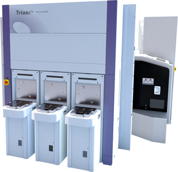
Tokyo Electron Limited (TEL) announced today that it will begin accepting orders for the Triase+TM EX-IITM TiN* Plus HT single-wafer metallization system in April 2016.
Its base model, the Triase+ EX-II TiN, is a high-speed single-wafer ASFD* system with an optimized reactor chamber and unique gas injection mechanism. Since its introduction in January 2013, the Triase+ EX-II TiN has established itself as the standard for single-wafer ASFD TiN metallization systems, and has been adopted by memory and logic device manufacturers throughout the world. The Triase+ EX-II TiN Plus, an upgraded model that became available for booking in July 2015, has also been enthusiastically received in the market.
The continued scaling of semiconductor technologies has required that TiN processes in advanced device manufacturing become more detailed and diverse than ever before. TiN deposition systems must now overcome new technical challenges at highly sophisticated levels.
The EX-II TiN Plus HT, which will soon be available to order, has specialized hardware for high-temperature processes and is capable of depositing TiN film of a lower resistance and lower impurity-key technical requirements for advancing semiconductor scaling. Customers already using the Triase+ EX-II TiN or the EX-II TiN Plus can upgrade to the EX-II TiN Plus HT by modifying their existing systems, thereby reducing investment costs.
"The Triase+ EX-II TiN Plus HT is the latest generation system in the series," said Takeshi Okubo, Executive Officer and General Manager, SDBU at TEL. "It is equipped to perform high-temperature processes to satisfy new technical requirements resulting from the scaling of semiconductors, while maintaining the excellent within-wafer uniformity and step coverage achieved by the preceding EX-II TiN Plus. TEL will keep tackling difficult technology development issues to deliver high value-added products for broad-ranging thin film deposition applications."
* TiN: Titanium Nitride; ASFD: Advanced Sequential Flow Deposition, a low-temperature processing method for forming nanoscale metal films with highly-engineered properties.
No comments:
Post a Comment