Earlier
this year this blog reported on expected growth for ALD OEMs due to
capital investments driven by 14 & 10 nm at TSMC and other Foundries
- 2016 will be a good year for the ALD Equipment Manaufacturers. Another
area that is rapidly introducing ALD processes is MEMS. Finnish ALD
Company Picosun is experiencing revenue from the MEMS Industry and sees a
big future growth opportunity in this area, having a competitive edge
by their batch ALD cluster tools.
In 2014, the MEMS sector represented an $11.1B business for Si-based devices according to Yole Développement (Yole) latest MEMS report “Status of the MEMS Industry”.
According to Yole, the MEMS industry is forecasted to exceed $20B by 2020 and lead by the “MEMS Titan” Robert Bosch (Bosch). Picosun and Bosch has a collaboration in ALD as announced in 2014 (http://www.picosun.com/sitenews/view/-/nid/117/ngid/4). So it indeed seems that Picosun is very well positioned to take on a lead as a Tier1 ALD MEMS supplier.
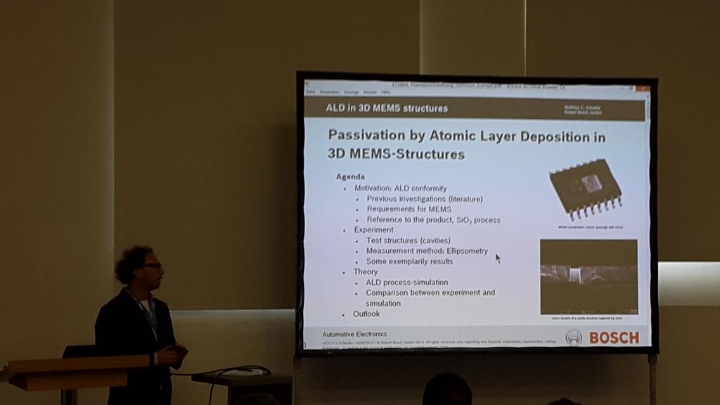
Passivation of MEMS by Atomic Layer Deposition, Matthias Schwille, Robert Bosch (ALD Lab Dresden Symposium, SEMICON Europa 2015)
Under this new analysis entitled, “Status of the MEMS Industry” report Yole proposes a deep understanding of the MEMS markets trends and players dynamics. The More than Moore market research and strategy consulting company announces its 2014 MEMS manufacturers and foundries ranking and proposes an overview of the future game-changers including new devices, disruptive technologies, 300mm wafers, sensor fusion and new markets.
As reported by Picosun: Picosun Oy, the leading supplier of high quality ALD (Atomic Layer Deposition) thin film coating solutions for industrial production, has revolutionized cost-effective MEMS manufacturing with high throughput PICOPLATFORM™ batch ALD cluster technology.
MEMS (MicroElectroMechanical Systems; Microsystems) are micrometer-scale, semiconductor-based components that combine e.g. electrical, mechanical, and optical functions. They are present in our everyday electronics in products such as hard disk read heads, inkjet printer nozzles, microphone and videoprojector chips, and airbag controls, tire pressure monitoring, and driving stability systems in cars.
Fast, fully automated and economically feasible batch processing without compromising the strictest process quality and purity requirements of the semiconductor industries is the prerequisite for industrial breakthrough of the next generation MEMS devices. They realize improved data storage, mobile phone, GPS positioning, and automotive control electronics, and health care applications such as body area sensors and remote monitoring devices. Combining batch ALD processing with fully automatic, robotized PICOPLATFORM™ vacuum cluster systems enables super-fast throughput of MEMS chips with excellent yield, process purity and uniformity levels(*).
Team Picosun
“Our MEMS customers gain immense benefits from our SEMI S2 certified PICOPLATFORM™ cluster technology. Equipped with our production-proven PICOSUN™ P-series batch ALD tools, these cluster systems have already proven their worth at the manufacturing sites of leading, global microsystems industries. Considering the MEMS market growth forecasts, propelled by the coming era of the Internet-of-Things, this product line will definitely be one of the cornerstones of our industrial ALD business,” states Mr. Timo Malinen, Chief Operating Officer of Picosun.
(*) Within-wafer, wafer-to-wafer, and batch-to-batch film thickness non-uniformity values (1σ) measured with 50 nm Al2O3 process on 200 mm Si wafers (25 wafers/batch) < 1%. The development work for batch ALD cluster technology has been performed in the project Lab4MEMS (1.1.2013 - 31.12.2015), coordinated by ST Microelectronics.
The project Lab4MEMS has received funding from the EC under the ENIAC Nanoelectronics Framework Programme (ENIAC-2012-2) under grant agreement no 325622-2.


%20(1).png)


nice blog and your informations are more impressive to me.Thanks for sharing this with us.
ReplyDeleteHadoop Training in Chennai
Big data training in chennai
Hadoop Training in Anna Nagar
JAVA Training in Chennai
Python Training in Chennai
Selenium Training in Chennai
Hadoop training in chennai
Big data training in chennai
big data course in chennai