Friday, July 31, 2015

Transparent, electrically conductive network of ALD encapsulated silver nanowires by HZB

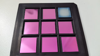
As reported by HZ Berlin (HZB) - A team headed by Prof. Silke Christiansen has developed a transparent electrode with high electrical conductivity for solar cells and other optoelectronic components – that uses minimal amounts of material. It consists of a random network of silver nanowires that is coated with aluminium-doped zinc oxide. The novel electrode requires about 70 times less silver than conventional silver grid electrodes, but possesses comparable electrical conductivity.

The electrodes for connections on the “sunny side” of a solar cell need to be not just electrically conductive, but transparent as well. As a result, electrodes are currently made either by using thin strips of silver in the form of a coarse-meshed grid squeegeed onto a surface, or by applying a transparent layer of electrically conductive indium tin oxide (ITO) compound. Neither of these are ideal solutions, however. This is because silver is a precious metal and relatively expensive, and silver particles with nanoscale dimensions oxidise particularly rapidly; meanwhile, indium is one of the rarest elements on earth crust and probably will only continue to be available for a few more years.

Mesh of silver nanowires


Manuela Göbelt on the team of Prof. Silke Christiansen has now developed an elegant new solution using only a fraction of the silver and entirely devoid of indium to produce a technologically intriguing electrode. The doctoral student initially made a suspension of silver nanowires in ethanol using wet-chemistry techniques. She then transferred this suspension with a pipette onto a substrate, in this case a silicon solar cell. As the solvent is evaporated, the silver nanowires organise themselves into a loose mesh that remains transparent, yet dense enough to form uninterrupted current paths.

 
Figure from graphical abstract (doi:10.1016/j.nanoen.2015.06.027)
 
Encapsulation by AZO crystals

Subsequently, Göbelt used an atomic layer deposition technique to gradually apply a coating of a highly doped wide bandgap semiconductor known as AZO. AZO consists of zinc oxide that is doped with aluminium. It is much less expensive than ITO and just as transparent, but not quite as electrically conductive. This process caused tiny AZO crystals to form on the silver nanowires, enveloped them completely, and finally filled in the interstices. The silver nanowires, measuring about 120 nanometres in diameter, were covered with a layer of about 100 nanometres of AZO and encapsulated by this process.
 

Published in Nano Energy, Vol. 16, Sept. 2015: "Encapsulation of silver nanowire networks by atomic layer deposition for indium-free transparent electrodes". Manuela Göbelt, Ralf Keding, Sebastian W. Schmitt,Björn Hoffmann, Sara Jäckle, Michael Latzel, Vuk V. Radmilović,Velimir R. Radmilović,Erdmann Spiecker, Silke Christiansen.
doi:10.1016/j.nanoen.2015.06.027

High-pressure anneal for indium gallium arsenide transistors with ALD HKMG

As reported by Semiconductor Today : Researchers in the USA and Korea have developed a hydrogen high pressure annealing (HPA) process for an ALD aluminium oxide/hafnium dioxide (Al2O3/HfO2) gate stacks on indium gallium arsenide (InGaAs) quantum wells [Tae-Woo Kim et al, IEEE Electron Device Letters, vol36, p672, 2015]. The aim of the team, from SEMATECH Inc in the USA, the Korea Advanced Nano Fab Center in South Korea, Poongsan Inc in the USA, and Kyungpook National University in South Korea, was to reduce interface and border traps that adversely affect transistor performance and threshold voltage reliability.


(a) Schematic cross-section for InGaAs MOSCAPs and MOSFETs with HPA, (b) energy-band diagram with interfacial and border traps, and (c) cross-sectional TEM images for ALD Al2O3/HfO2 gate stack before and after HPA.

Full story: http://www.semiconductor-today.com/news_items/2015/jul/sematech_280715.shtml

Thursday, July 30, 2015

ASM International reports strong demand for ALD tools

The number one ALD company in sales (Gartner, 2014) ASM International reports the second quarter 2015 results:


  • Net sales for the second quarter 2015 were €201 million, an increase of 24% compared to the previous quarter. Year-on-year net sales increased with 35%. 
  • New orders at €167 million were 5% above the Q1 2015 level. 
  • Normalized net earnings for the second quarter 2015 decreased by €20 million compared to the first quarter 2015, due to a €40 million lower currency effect on cash held in foreign currencies, especially US dollar. Excluding those currency effects normalized net earnings increased from €39 million to €59 million. The result from investments increased with €7 million. 

Commenting on the results, Chuck del Prado, President and Chief Executive Officer of ASM International said: 

"Q2 2015 was again a strong quarter for ASMI. We realized revenues of €201 million, a sales increase of 24% over Q1 2015. Gross Margin improved further to more than 45%. Atomic Layer Deposition demand remained strong across a broad customer base. Our order intake remained healthy and was €167 million, 5% above the Q1 2015-level."

Wednesday, July 29, 2015

>10,000 visitors in July 2015 to the BALD Blog

In July there was more than 10,000 visitors already now with still some time left, which is a all time record. All in all I had soon 75,000 visitors since the start from 102 different countries! This is very rewarding and I would hope to do this permanently one day.


Considering the summer months June to August last year had a slow down in visitor and that all the Finns are out on vacation and have dropped out of the monthly top 10 list for the first time I think that I must be very happy with the visitor statistics for the summer 2015 so far. Somehow I managed to keep a growth also over summer which I am very happy for! Both the ALD 2015, EuroCVD, SEMICON West and Angela Merkels visit to Dresden has contributed that that fore sure. 


Another page that has been very successful so far is the Job page. If didn´t know about it until now you can find it here and you are most welcome to submit ALD jobs directly to me and I will post them for you - It is for free!


A big thank you to all blog visitors and I hope you all come back next month and please feel free to bring your friends! Tack så mycket! :-)


Helmholtz to invest 46 million EUR in a Energy Materials Foundry (HEMF)

Six Helmholtz Centres are founding a shared infrastructure for developing novel energy materials that will also be available to external users. The Helmholtz Senate has approved setting up a major infrastructure to synthesise and develop novel systems of materials for energy conversion and storage. Total funding will be 46 million EUR (2016-2020).


The Helmholtz Association performs cutting-edge research which contributes substantially to solving the grand challenges of science, society and industry. Scientists at Helmholtz concentrate on researching the highly-complex systems which determine human life and the environment. For example, ensuring that society remains mobile and has a reliable energy supply that future generations find an intact environment or that treatments are found for previously incurable diseases. The activities of the Helmholtz Association focus on securing the foundations of human life long-term and on creating the technological basis for a competitive economy. The potential with which the Association achieves these goals is made up of the outstanding scientists working at the research centres, a high-performance infrastructure and modern research management.

The Helmholtz Energy Materials Foundry (HEMF) will be coordinated by the Helmholtz-Zentrum Berlin, while five additional Helmholtz Centres are participating in the design, planning, and setup: the German Aerospace Center (DLR), Forschungszentrum Jülich (FZJ), Helmholtz-Zentrum Geeshacht (HZG) for Materials and Coastal Research, Helmholtz-Zentrum Dresden-Rossendorf (HZDR), and the Karlsruhe Institute of Technology (KIT). The HEMF platform will also be open to external users from universities and non-university institutes from Germany and abroad, as well as to industry.

Several outstanding supplementary laboratories with unique equipment will be set up under HEMF at the six participating Helmholtz Centres. The scientific focus lays on the design of energy materials associated with solar fuels, solar cells, and battery systems as well as thermoelectric and thermochemical materials. One research topic these applications share is the design of novel catalysts to be employed in energy conversion and storage.


Hermann Ludwig Ferdinand Helmholtz born in Potsdam 1821 studied at the Berlin Military Academy and gained his Doctor of Medicine in 1842.  He took the chair of physiology and pathology in Königsberg on the recommendation of Alexander von Humboldt, which he held until 1855. Other chairs followed, in Bonn (1855 to 1858) and Heidelberg (1858 to 1871). From 1871, Helmholtz became professor of physics and taught at the University of Berlin. In the late 1880s, he became the founding president of the Physikalisch-Technische Reichsanstalt in Charlottenburg, which he himself and Werner von Siemens had established and which continues even today - as the Physikalisch Technische Bundesanstalt (PTB) - to serve the science of metrology.

The range of capabilities of the HEMF platform extends from the design of novel materials systems, to in-situ and in-operando analyses of processes for their synthesis, and three-dimensional nanostructuring of these materials to alter their properties in specific ways. In addition, new methods will be developed to process novel materials, produce innovative prototypes for specific applications, and investigate their properties and capabilities under continuous loads. “This comprehensive approach enables creation of efficient feedback loops between synthesis, characterisation, and the evaluation of the end products. It will help us accelerate knowledge-based development”, says Prof. Anke Kaysser-Pyzalla, Scientific Director of HZB.


HZB’s BESSY II facility in Berlin

Synthesis laboratories are planned at HZB specifically for perovskite thin films, nanoparticles for catalysis and electrochemical storage, as well as facilities for nanostructuralisation of materials. New methods will be developed for studying electrochemical processes at catalytic and heterogenous boundary surfaces by the Energy Materials in-situ Laboratory (EMIL) recently set up at HZB’s BESSY II facility. Moreover, testing labs are also being set up in order to study new systems of materials under actual operating conditions. HZB is working together on this with the Max Planck Society’s Fritz Haber Institute in Berlin and the Max Planck Institute for Chemical Energy Conversion (CEC) in Mülheim.

The HEMF platform will be operated as an international user facility. The laboratories will be available to research teams from universities, non-university research institutions, and industry. The coordination of user operations will be handled by HZB, which has a great deal of experience with this and has built up outstanding user services for its own large-scale facilities BESSY II and BER II. About 3000 external personnel visiting for purposes of conducting measurements benefit from these services annually. HEMF builds on the model of Berkeley Labs in California, where a Molecular Foundry was also set up as an infrastructure serving international user groups.


HZDR in Rossendorf in the forest west of Dresden

“HEMF will augment the Helmholtz Association’s expertise in synthesis of raw materials indispensable for the energy transition. The participating Helmholtz Centres will be able to add their research capabilities to this shared infrastructure so that we can make the energy we will need in the future available for use in a safe and simultaneously environmentally friendly way. At the same time, the platform will draw attractive collaborating partners who are pursuing the same research goals”, Kaysser-Pyzalla explains further. This research plan’s unique order of magnitude will help the group of Helmholtz Centres contribute R&D on new energy materials – a contribution that will be comparably large and pioneering on an international scale as well.


A cluster vacuum tool at the ion beam center at HZDR.

According to this report by Heiko Weckbrodt (Computer Oiger) Helmholtz-Zentrum Dresden-Rossendorf (HZDR) will invest 3,5 M Euro in the existing Ion beam center and a new lab for nano lithography and analytics.

Intel and Micron Produce Breakthrough Memory Material & Arcitecture

According to the recent press release Intel and Micron are about to begin production on new class of non-volatile memory (NVM). TThe claim that this is "the first new memory category in more than 25 years."

Intel and Micron invented unique material compounds and a cross point architecture for a memory technology that is 10 times denser than conventional memory. (Photo: Business Wire)

  • New 3D XPoint™ technology brings non-volatile memory speeds up to 1,000 times faster than NAND, the most popular non-volatile memory in the marketplace today.
  • The companies invented unique material compounds and a cross point architecture for a memory technology that is 10 times denser than conventional memory2.
  • New technology makes new innovations possible in applications ranging from machine learning to real-time tracking of diseases and immersive 8K gaming.


New architecture... cross point architecture... think I heard that one before... an ants nest is also cross bar architecture...  hmmm not that interesting but more interesting so is what is this invented unique material and what processes are used for manufacturing? So we need to read the complete press release.


"The innovative, transistor-less cross point architecture creates a three-dimensional checkerboard where memory cells sit at the intersection of word lines and bit lines, allowing the cells to be addressed individually. As a result, data can be written and read in small sizes, leading to faster and more efficient read/write processes."

Transistor less - first clue! Continue reading... Cross Point Array Structure, Stackable, Selector, Fast Switching Cell, ... ??? What is the new unique material? How was it processed? How was it etched? Need to know... I´ll be back.

"Bulk switching characteristics"

BINGO! Peter Clarke at EE Times had it all in better detail - Intel, Micron Launch "Bulk-Switching" ReRAM.

"The prepared infographics suggest a resistive RAM with an in-built select diode allowing for a dense device structure. This would give it similarities to ReRAMs being developed by Crossbar Inc. (Santa Clara, Calif.) and other companies but would still leave a potential point of distinction — filamentary behavior." 

"Micron's Durcan said: "We are not the only companies thinking of bringing resistive elements to memory, but ours is unique." Intel's Cooke said the memory has the three attributes of: non-volatility, density and speed and that the memory scales in both the x-y plane and the z direction."

"Intel did confirm that 3D XPoint manufacturing is compatible with back-end-of-line (BEOL) processing, which opens up the possibility of deploying 3D Xpoint memory on top of a plane of logic and as an embedded non-volatile memory option."

In the commentary field Peter Clarke says: "I can only add that in the webcast press conference Rob Crooke and Mark Durcan emphasize repeatedly a switching electrical characteristic that occurred across the "bulk" of the memory cell material. They also talked about the cells being "completely different" to other non-volatile memories; "a fundamentally different switch" and a "fundamental discovery"

Check ou the Intel / Micron Webcast below


So still no information out there on the actual material stack and the deposition processes - obviously the whole ALD World is keeping their fingers crossed that this one like DRAM and modern CMOS can only be made by A-L-D!!!

Tyndall propose an new metallocene reducing agent pathway for ALD of copper

The Materials Modelling For Devices group headed by Simon Elliott at Tyndall National Institute, University College Cork propose using metallocene compounds as reducing agents for atomic layer deposition (ALD) of the transition metal Cu from metalorganic precursors resulting in a new pathway for ALD of copper. The screening results of 10 different compunds has been published in Dalton Transactions recently and generated the status - Hot Article!


Quantum chemical and solution phase evaluation of metallocenes as reducing agents for the prospective atomic layer deposition of copper 

Gangotri Dey, Jacqueline S. Wrench, Dirk J. Hagen, Lynette Keeney and Simon D. Elliott
Dalton Trans., 2015,44, 10188-10199
DOI: 10.1039/C5DT00922G 


We propose and evaluate the use of metallocene compounds as reducing agents for the chemical vapour deposition (and specifically atomic layer deposition, ALD) of the transition metal Cu from metalorganic precursors. Ten different transition metal cyclopentadienyl compounds are screened for their utility in the reduction of Cu from five different Cu precursors by evaluating model reaction energies with density functional theory (DFT) and solution phase chemistry.


Monday, July 27, 2015

Hynix high bandwidth memory in an AMD Radeon ALD High-k Fury

Check it out - this is like the coolest thing I have ever seen so far - the two leading ALD High-k products (DRAM & High performance CMOS) merged into one ultra high performance graphics chip by AMD. TechInsights has investigated the AMD Fury X cards in their lab  and published it in a series of articles in EE Times:

The Hunt for Hynix HBM - Hynix high bandwidth memory addresses bandwidth limitations


Accordingly, SK Hynix announced its high bandwidth memory (HBM) product in early 2014, claiming it to be the world’s first 8Gb module made using 2Gb, 20nm node, DDR4 SDRAM. Now the HBM modules has shown up in product - AMD’s Radeon 390X Fury X graphics card.


According to TechInsight : "Hynix disclosed a via middle process for their HBM in two papers (Electronics Components & Technology Conference 2013 and VLSI Tech. Digest 2014). The TSV openings are formed after the tungsten contacts to the gates and source/drain regions are made, using a Bosch TSV etch. An oxide liner is then deposited along the via sidewalls, lined with a Ta-based barrier and Cu seed layers, and filled with electroplated Cu. A thermal anneal process is used as a Cu stress relief. A CMP and etch process is used to thin the backsides of the DRAM wafer and expose the Cu TSVs. The backsides of the DRAM wafers are then passivated with oxide, followed by the formation of the backside micro bumps."


AMD Radeon Fury X (Source: TechInsights)


Some facts from the reports:

  • The GPU die has four Hynix HBM memory modules arranged around its perimeter. 
  • Both the GPU and the HBM modules are flip-chip bumped to a UMC fabbed interposer. 
  • The interposer is, in turn, bumped to a laminate substrate. 
  • The GPU itself is a massive measuring in at 23mm by 27mm large, and is believed to be fabricated using TSMC’s 28nm HKMG process.


"The GPU die is seen in the center of the module with four Hynix HBM memory modules arranged around its perimeter. Both the GPU and the HBM modules are flip-chip bumped to a UMC fabbed interposer. This interposer is, in turn, bumped to a laminate substrate. The GPU is massive measuring in at 23mm by 27mm large, and is believed to be fabricated using TSMC’s 28nm HKMG process." (EE Times, TechInsight)


Schematic cross section of HBM module. (Source: AMD HBM brochure, TechInsights)


Hynix HBM memory (Source: Package Analysis of the SK-Hynix HBM, TechInsights)


Sunday, July 26, 2015

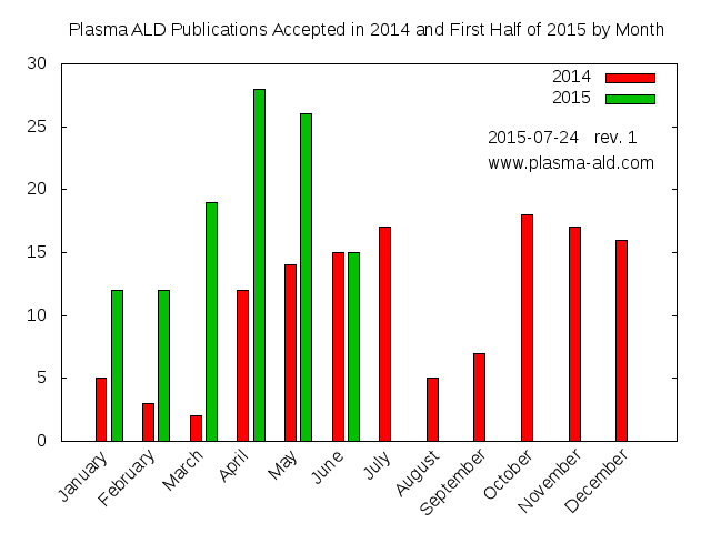
Growth in Plasma ALD publication for first half of 2015

Plasma-ALD.com reports that there is a clear increase in Plasma ALD publication in the first had of 2015 as compared to 2014 "Through the first six months of 2015, I have collected 112 PEALD publications. Compared to the 51 for this same time period in 2014, this represents a 120% growth. Exciting news for the PEALD community. Now I need to find the time to review them all and get them into the plasma ALD Publication Database."


This confirms the general trend seen that ALD is being used more and more for low thermal budget applications in patterning as well as BEOL and non-semiconductor fields. Also I have heard directly from ALD OEMs that the sales in PEALD has increased lately. Today most OEMs offer a PEALD chamber technology. 

Another clear sign that PEALD is coming strong is that there is actually an after market in converting thermal ALD chambers to PEALD. One such company is Meaglow that offer Plasma upgrades of PEALD chambers as well as complete conversion kits from thermal ALD to PEALD.


Ultra-Thin Hollow Nanocages Could Reduce Platinum Use in Fuel Cell Electrodes

As reported by Georgia Tech : A new fabrication technique that produces platinum hollow nanocages with ultra-thin walls could dramatically reduce the amount of the costly metal needed to provide catalytic activity in such applications as fuel cells.


The technique uses a solution-based method for producing atomic-scale layers of platinum to create hollow, porous structures that can generate catalytic activity both inside and outside the nanocages. The layers are grown on palladium nanocrystal templates, and then the palladium is etched away to leave behind nanocages approximately 20 nanometers in diameter, with between three and six atom-thin layers of platinum.


Use of these nanocage structures in fuel cell electrodes could increase the utilization efficiency of the platinum by a factor of as much as seven, potentially changing the economic viability of the fuel cells.

“We can get the catalytic activity we need by using only a small fraction of the platinum that had been required before,” said Younan Xia, a professor in the Wallace H. Coulter Department of Biomedical Engineering at Georgia Tech and Emory University. Xia also holds joint faculty appointments in the School of Chemistry and Biochemistry and the School of Chemical and Biomolecular Engineering at Georgia Tech. “We have made hollow nanocages of platinum with walls as thin as a few atomic layers because we don’t want to waste any material in the bulk that does not contribute to the catalytic activity.”

The research – which also involved researchers at the University of Wisconsin-Madison, Oak Ridge National Laboratory, Arizona State University and Xiamen University in China – was scheduled to be reported in the July 24 issue of the journal Science.


Friday, July 24, 2015

Video of a Visionox rollable OLED display in production 2017

OLED-Info just uploaded this amazing video of a truly rollable OLED display soon to go into mass production 2017 at Visionox in Mainland China - I do wonder if they use an ALD barrier to reach 3 mm curvature.


Thursday, July 23, 2015

EUV, Atomic Layer Processes and KLA to solve all all Fab Issues at 7 nm and 5 nm

Here is yet another great article in Semiconductor Engineering by Mark Lapedus on the "The race toward the 7nm logic node. He systematically go through and summarize all important issues and technologies and news from SEMICON West from EUV via ALD to KLA ;-)


New technologies after finFETs and how the industry is likely to get there if it can resolve some very tough issues.

The race toward the 7nm logic node officially kicked off in July, when IBM Research, GlobalFoundries and Samsung jointly rolled out what the companies claim are the industry’s first 7nm test chips with functional transistors.

They’re not alone, of course. Intel and TSMC also are racing separately to develop 7nm technology. And in the R&D labs, chipmakers also are working on technologies for 5nm and beyond. Needless to say, the timing and certainty of 7nm and 5nm remain unclear.

In any case, there are two basic transistor candidates at 7nm—the finFETand the lateral gate-all-around nanowire FET, sometimes called the lateral nanowire FET. And at 5nm, the industry is leaning towards the lateral nanowire FET.

[...]
  • Patterning and mask making - EUV, LER
  • Fab flow and variation - CMP
  • Selective processes - ALD, MLD, ALE
  • Interconnects - RC
  • Inspection and metrology - KLA
While you´re at it you should also read this article by Mark Lapedus : 

What Will 7nm And 5nm Look Like? - Delays at 10nm raise questions about what’s next.

http://semiengineering.com/moores-law-slips-again/

Today, the lateral nanowire FET is the sole option at 5nm, according to Imec. Vertical FETs, TFETs and the other technologies have been pushed out to 3nm (!)

First Atomic Layer Etch experiments at Lund Nano Lab

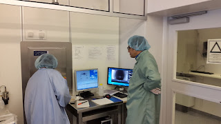
An exciting day today in the middle of Swedish vacation times as we made the first experience with Atomic Layer Etching (ALE) at Lund Nano Lab.


Reza Jafari Jam instructing us and learning all the tricks on etching with the Oxford PlasmalabSystem 100.


We use a Oxford Instrument PlasmalabSystem 100 and the rather well studied Ar-plasma- Purge-Cl2-Purge sequence to etch silicon form the device layer of a 300mm FD-SOI wafer that we diced up in 10x10 mm coupons


Our Master student on ALE Sabbir Khan adjusting the first recipe that Dmitry Suyantin wrote before going on a well deserved vacation


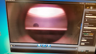
The first plasma cycle - you can almost sense the saturation here ...


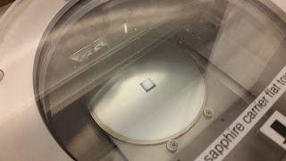
Unloading the first sample after 10 ALE cycles - looks pretty much like we have removed some Ångströms per cycle here - how many we will have to see when the elipsometer model for the stack is put to test.


Pristine 10x10 mm SOI coupon samples next to the etched one - elipsometer tells us we removed 2-3 Å but the fit is really bad so we need to get that reconfirmed later.

Stay tuned for more updates and yes we will move to etching III/V nanowires as soon as we can say that we master etching silicon layer by layer.

The 37th Int Symposium on Dry Process (DPS2015) in Japan November 5 & 6

The 37th International Symposium on Dry Process (DPS2015) will be held at Awaji Yumebutai International Conference Center, Awaji Island, in Japan, on November 5 & 6, 2015. This year there are a number of interesting talks by invited speakers on Atomic Layer Etching (ALE) form TU Eindhoven, Lam Research, Applied Materials. (Thanks Sabbir Khan for sharing)

The Symposium covers all aspects of the rapidly evolving fields of dry processes, including but not limited to plasma etching and deposition processes, diagnostics and modeling of plasmas and surfaces, and surface modifications by plasmas, for the applications in, e.g., microelectronics, power devices, sensors, environmental protection, biological systems, and medicine. The DPS has provided valuable forums for in-depth discussion among professionals and students working in this exciting field for more than three decades.


Invited speakers and tentative titles(Tentative)

  • Dr. Sebastian Engelmann (IBM Thomas J. Watson Research Ctr.)
    "Improving high aspect ratio processes for logic applications through gas chemistry and plasma discharge optimization"
  • Prof. Erwin Kessels (The Eindhoven University of Technology)
    "Atomic layer deposition and etching: progress and prospects"
  • Dr. Chris Lee (Lam Research Corporation)
    "Challenges of Atomic-layer processing: an industry perspective"
  • Dr. Hirokazu Ueda (Tokyo Electron Ltd. )
    "Conformal doping using a radial line slot antenna microwave plasma source"
  • Dr. Peter Ventzek (Tokyo Electron America, Inc.)
  • Dr. Ying Zhang (Applied Materials Inc.)
    "A New Frontier of Plasma Patterning: Atomic Layer Etch"

Wednesday, July 22, 2015

Oak Ridge researchers make scalable arrays of building blocks for ultrathin electronics

OAK RIDGE, Tenn., July 22, 2015--Semiconductors, metals and insulators must be integrated to make the transistors that are the electronic building blocks of your smartphone, computer and other microchip-enabled devices. Today's transistors are miniscule--a mere 10 nanometers wide--and formed from three-dimensional (3D) crystals.


Complex, scalable arrays of semiconductor heterojunctions -- promising building blocks for future electronics -- were formed within a two-dimensional crystalline monolayer of molybdenum deselenide by converting lithographically exposed regions to molybdenum disulfide using pulsed laser deposition of sulfur atoms. Sulfur atoms (green) replaced selenium atoms (red) in lithographically exposed regions (top) as shown by Raman spectroscopic mapping (bottom). Credit : Oak Ridge National Laboratory, U.S. Dept. of Energy

But a disruptive new technology looms that uses two-dimensional (2D) crystals, just 1 nanometer thick, to enable ultrathin electronics. Scientists worldwide are investigating 2D crystals made from common layered materials to constrain electron transport within just two dimensions. Researchers had previously found ways to lithographically pattern single layers of carbon atoms called graphene into ribbon-like "wires" complete with insulation provided by a similar layer of boron nitride. But until now they have lacked synthesis and processing methods to lithographically pattern junctions between two different semiconductors within a single nanometer-thick layer to form transistors, the building blocks of ultrathin electronic devices.

Now for the first time, researchers at the Department of Energy's Oak Ridge National Laboratory have combined a novel synthesis process with commercial electron-beam lithography techniques to produce arrays of semiconductor junctions in arbitrary patterns within a single, nanometer-thick semiconductor crystal. The process relies upon transforming patterned regions of one existing, single-layer crystal into another. The researchers first grew single, nanometer-thick layers of molybdenum diselenide crystals on substrates and then deposited protective patterns of silicon oxide using standard lithography techniques. Then they bombarded the exposed regions of the crystals with a laser-generated beam of sulfur atoms. The sulfur atoms replaced the selenium atoms in the crystals to form molybdenum disulfide, which has a nearly identical crystal structure. The two semiconductor crystals formed sharp junctions, the desired building blocks of electronics. Nature Communicationsreports the accomplishment.

"We can literally make any kind of pattern that we want," said Masoud Mahjouri-Samani, who co-led the study with David Geohegan. Geohegan, head of ORNL's Nanomaterials Synthesis and Functional Assembly Group at the Center for Nanophase Materials Sciences, is the principal investigator of a Department of Energy basic science project focusing on the growth mechanisms and controlled synthesis of nanomaterials. Millions of 2D building blocks with numerous patterns may be made concurrently, Mahjouri-Samani added. In the future, it might be possible to produce different patterns on the top and bottom of a sheet. Further complexity could be introduced by layering sheets with different patterns.

Added Geohegan, "The development of a scalable, easily implemented process to lithographically pattern and easily form lateral semiconducting heterojunctions within two-dimensional crystals fulfills a critical need for 'building blocks' to enable next-generation ultrathin devices for applications ranging from flexible consumer electronics to solar energy."


Tuning the bandgap


"We chose pulsed laser deposition of sulfur because of the digital control it gives you over the flux of the material that comes to the surface," said Mahjouri-Samani. "You can basically make any kind of intermediate alloy. You can just replace, say, 20 percent of the selenium with sulfur, or 30 percent, or 50 percent." Added Geohegan, "Pulsed laser deposition also lets the kinetic energy of the sulfur atoms be tuned, allowing you to explore a wider range of processing conditions."

It is important that by controlling the ratio of sulfur to selenium within the crystal, the researchers can tune the bandgap of the semiconductors, an attribute that determines electronic and optical properties. To make optoelectronic devices such as electroluminescent displays, microchip fabricators integrate semiconductors with different bandgaps. For example, molybdenum disulfide's bandgap is greater than molybdenum diselenide's. Applying voltage to a crystal containing both semiconductors causes electrons and "holes" (positive charges created when electrons vacate) to move from molybdenum disulfide into molybdenum diselenide and recombine to emit light at the bandgap of molybdenum diselenide. For that reason, engineering the bandgaps of monolayer systems can allow the generation of light with many different colors, as well as enable other applications such as transistors and sensors, Mahjouri-Samani said.

Next the researchers will see if their pulsed laser vaporization and conversion method will work with atoms other than sulfur and selenium. "We're trying to make more complex systems in a 2D plane--integrate more ingredients, put in different building blocks--because at the end of the day, a complete working device needs different semiconductors and metals and insulators," Mahjouri-Samani said.

To understand the process of converting one nanometer-thick crystal into another, the researchers used powerful electron microscopy capabilities available at ORNL, notably atomic-resolution Z-contrast scanning transmission electron microscopy, which was developed at the lab and is now available to scientists worldwide using the Center for Nanophase Materials Sciences. Employing this technique, electron microscopists Andrew Lupini and visiting scientist Leonardo Basile imaged hexagonal networks of individual columns of atoms in the nanometer-thick molybdenum diselenide and molybdenum disulfide crystals.

"We could directly distinguish between sulfur and selenium atoms by their intensities in the image," Lupini said. "These images and electron energy loss spectroscopy allowed the team to characterize the semiconductor heterojunction with atomic precision."


Institute of Solid State Physics at the Bulgarian Academy of Sciences installs ALD and PECVD

The European Seventh Framework Program has funded purchase and installation of several advanced process tool at the Institute of Solid State Physics at the Bulgarian Academy of Sciences. 
  • Beneq TFS 200 Atomic layer Deposition
  • PECVD Oxford Nanofab Plasmalab System 100
INERA Open Days will take place at the Institute of Solid State Physics (BAS) during October 16 – 17, 2015.


The planed event will be designed to ensure that the visitors get detailed information about the project and its progress. They will have the opportunity to visit laboratories, listen to presentations on scientific novelties in different research fields of nanotechnology and its applications and discuss current topics with scientists from the Institute and its Partners within the project.

For more information on the equipment purchased within the framework of the European project INERA click here: http://www.inera.org/research-equipment/


The newly purchased within the framework of the European project INERA, Beneq TFS 200 (above) is a flexible ALD platform designed for research and development. Direct thermal and plasma ALD operation and remote plasma-enhanced deposition (PEALD) are available in the TFS 200 as a standard option. The plasma is capacitively-coupled (CCP), which is the industry standard nowadays. The TFS 200 is capable of coating planar objects and complex 3D shapes with very high aspect ratio features. TFS 200 has unique precursor capabilities of temperature rating up to 400. A total of 6 different gas lines, 4 liquid sources and 3 hot sources fulflil the most demanding requirements.

Available precursors are: DEZ (Diethyl zinc), TMA (Trimethyl aluminum), BTBAS ((Bis(tertiary-butyl- amino)silane)), Ferrocene (bis(η5-cyclopentadienyl)iron), Cobaltocene (Bis(η5-cyclopentadienyl)cobalt), Nickelocene ((Bis(cyclopentadienyl) nickel(II)).

Preliminary tests of pristine and doped ZnO thin films on deposition Al2O3 were successfully performed.


The PECVD system of Oxford Instruments (above)“Nanofab Plasmalab System 100” is a modern multi-purpose tool for various CVD and PECVD processes. The system has a vacuum loadlock and is designed for 2” – 8” wafer or other substrates. The maximal temperature of the substrate holder is 1200 °C which is suitable for deposition of graphene. Both radio-frequency (MHz) and low-frequency (kHz) plasma can be generated in the reaction chamber. The system is equipped with 6 gas lines which allows a variety of chemical processes. In the framework of the project INERA the tool will be used for growth of graphene and carbon nanotubes. 


These modern equipments are installed in a clean room class 10 000 with an area of about 40 m2 (above).


Tuesday, July 21, 2015

Lab-scale roll-to-roll ALD on textile by Tyndall

ALD growth is unstoppable - There is no end to it "The area certainly seems to show no sign of slowing down" as Maryn Pemble just commented on recent post regarding the latest growth forecast on ALD. Little did I know then while reading it the Tyndall just demonstrated ALD on textile in a spatial roll to roll machine! 


Last year I sat in a meeting with one of Europe's leading coating companies on the topic of ALD on textile and we discussed this topic back and forth if there is a market for it and if it can be done in a roll to roll system. Guess who I will be calling tomorrow morning!


Professor Martyn Pemble, Tyndall National Institute, University College Cork, Ireland (source).

Here are some textile/fibre related posts from the past year - ALD on textile is coming that´s for sure but do check out the video down below from Martyn Pemble and co-workers at Tyndall before!

From Youtube: This movie shows a lab-scale roll-to-roll atomic layer deposition (ALD) system which has been constructed at the Tyndall National Institute, University College Cork, Ireland, by Dr Shane O'Brien and Dr Ian Povey, using funding from Enterprise Ireland and Science Foundation Ireland.


Dr O'Brien and Dr Povey are based in the Advanced Materials and surfaces Group led by Prof Martyn E Pemble. The movie shows the textile sample moving forwards and backwards under the coating heads which supply the ALD precursors. The process is an example of so-called spatial ALD, whereby the precursors are separated spatially rather than in a temporal mode.

For further information please contact Prof Pemble using martyn.pemble@tyndall.ie or go to:

... and did you have enough? No, no I didm´t think so! It turns out that Prof. Pemble is involved in yet another roll to roll ALD project with a team from Sao Paolo, Brazil - check it out!


Designed and built by our colleagues at the university of Sao Paolo, Brazil (Prof Roberto Faria, Mr Leonardo Dias-Cagnani and Ms Giovana Americo-Rosso), this system is currently being used to prepare organic photovoltaics (OPV) and organic LEDs (OLEDs) on flexible transparent polymeric materials. This work is funded by SFI International Strategic Cooperation Award (ISCA) Brazil for which Tyndall are the lead partners in the area of nano materials.


The Nucleation Dependent Growth Layer: A Structure Element in Electrocrystallization - The 10th William Blum Lecture 1969

I was scaning the internet on Kolschuetter and "Atomic Layer" hoping finding proof on the pre-1950´s discovery of ALD (sorry) and came across this rather interesing reviw paper for a lecture in 1969 - Bunching and debunching effects very fascinating indeed and just look how the images and graphs, which are so much more beautiful than today!

"This paper is a re-publication of the 10th William Blum Lecture, presented at the 56th AES Annual Convention in Detroit, Michigan, on June 16, 1969. Prof. Dr. Hellmuth Fischer discussed his work on the theory of plating and how the electrochemistry and use of additives in the bath led to different types of deposit structure"
 
Prof. Dr. Hellmuth Fischer
Recipient of the 1968 William Blum AES Scientific Achievement Award


Originally published as Plating, 56 (11), 1229-1233 (1968).

Editor’s Note: This paper is a re-publication of the 10th William Blum Lecture, presented at the 56th AES Annual Convention in Detroit, Michigan, on June 16, 1969.  A printable PDF version is available by clicking HERE.
ABSTRACT
For the first time, it has been shown by Eichkorn that layer growth (not of growth-spirals) depends on continued nucleation of monoatomic layers building up growth layers.  This has been done by determination of nucleation-overvoltage η and thickness of growth layers.  During formation of growth layers, overvoltage must surpass η and time dependent adsorption of foreign substances must control the motion rate of monoatomic layers.  Growth layers can develop to whiskers, columnar crystals, fiber textures, twinned or randomly dispersed structures.


Subsequent nucleation, outgrowth and "bunching" of atomic layers forming a macrostep.


Articles on ALD following SEMICON West 2015

Here are some interesting articles on ALD following SEMICON West 2015. I don´t know what you think but it seems to me that ALD really went one step further 2015! I will update as I find more and if you have seen anything interesting please let me know! (jonas.sundqvist@baldengineering.com)

Semicon West: Forget microelectronics it’s not even nano let’s call it atomtronics

The era of atomic level control of electrical properties have already begun, in that sense the so-called Moore’s law will continue but with the new way of doing things. The researchers in semiconductor manufacturing are both engineers and also equally good material scientists who always explored how to find a way around the technology barricades/walls and also design a manufacturing process in such a way that it can be manufactured in volumes at a cost feasible for business success. So it takes a huge amount of scientific as well as engineering talent and also business knowledge of the industry in this field of semiconductor research.

--------------------------------------------------------------------------

Dealing With Atoms


To process chips at the atomic level, there are various solutions in the market today. For years, ALD has been used to scale the capacitor in DRAMs as well as to develop the high-k/metal-gate stack for logic devices. More recently, ALD is also being used to deposit films for the spacers in multiple patterning applications.

In total, the ALD business is expected to reach $920 million to $925 million in 2015, up from $830 million in 2014, according to Applied Materials. Applied Materials, ASMI, Lam, TEL and others compete in the ALD tool market.

ALD is a deposition technique that deposits materials one layer at a time. “ALD is the alternation of two different chemistries being introduced in a sequential manner,” said David Chu, strategic marketing director at Applied Materials. “Because the chemistries are being broken up, it’s self-limiting. That’s why it allows the technology to be conformal.”

-------------------------------------------------------------------------- 

 Growth forecast for Wafer Fab Equipment and ALD according to Gartner

Good news of ALD - Gartner has forecasted a growth for the Advanced nodes to come!
Gartner says that the Worldwide semiconductor revenue is forecast to reach $348 billion in 2015, a 2.2 percent increase from 2014, but down from the previous quarter's forecast of 4.0 percent growth, according to Gartner, Inc.
Growth forecast for Wafer Fab Equipment according to Gartner (Graph from ASMi Investor Technology Seminar at SEMICON West)
 Continue reading : http://baldengineering.blogspot.se/2015/07/growth-forecast-for-wafer-fab-equipment.html

--------------------------------------------------------------------------

Imec introduces self-assembled monomolecular organic films to seal ultra-porous low- k materials

Nano-electronics research center imec announced today at SEMICON West that it has demonstrated concept and feasibility for pore-sealing low-k dielectrics in advanced interconnects. The method, based on the self-assembly of an organic monolayer, paves the way to scaling interconnects beyond N5. 


RC plot and HAADF-STEM images illustrating the effectiveness of SAM sealing in preventing metal indiffusion into the ultra-porous low-k film integrated in a 45nm half pitch dual damascene test vehicle. This translates in a 30% decrease in the measured capacitance. (www.imec.be)
 Continue reading : http://baldengineering.blogspot.se/2015/07/imec-introduces-self-assembled.html

--------------------------------------------------------------------------

UPDATE: ASM International technology briefing SEMICON West 2015

ASM International N.V.  announces that it will be hosting an analyst and investor technology briefing on Wednesday, July 15, 2015 at 8:00 - 9:30 a.m. (PDT) in San Francisco, US, coinciding with SEMICON West 2015. The presentation will be held in Room 301, Esplanade, Moscone Center.
 
ASMi is operating in a very close relationship with leading IDMs and Imec on CMOS scaling. In this technology seminar Han Westendorp, Vice President Corporate Marketing, will present "Advanced wafer processing with new materials". The presentation will include highlights of ASM's 
  • Advanced thermal ALD
  • Plasma enhanced ALD products and technologies
  • CVD, PECVD and epitaxy technologies
Continue reading: http://baldengineering.blogspot.se/2015/07/asm-international-will-be-hosting.html

-------------------------------------------------------------------------- 

Lam Research Releases High-Productivity VECTOR(R) ALD Oxide Deposition System

Lam Research Corp a major global supplier of innovative wafer fabrication equipment and services to the semiconductor industry, today announced it has released its high-productivity VECTOR® ALD Oxide system on the Extreme platform. The new product uses atomic layer deposition (ALD) to create highly conformal dielectric films with an emphasis on advanced patterning, in particular spacer-based multiple patterning. One key challenge is managing thickness variability of the self-aligned spacers that define critical dimensions (CDs). By delivering superior CD control, VECTOR ALD Oxide has been winning volume-production decisions for multi-patterning applications. Now leveraging Lam's Extreme platform, the latest system meets productivity requirements for continued scaling, where additional steps increase process time, cost, and complexity. As a result, VECTOR ALD Oxide is gaining rapid adoption by a number of leading chipmakers for advanced multi-step patterning applications.


"Multiple patterning continues to be a key inflection for the industry, and spacer-based multi-patterning remains an enabling strategy for chipmakers for both current immersion and future EUV lithography schemes," said Sesha Varadarajan, group vice president, Deposition Product Group. "With this in mind, we are working closely with our customers to deliver cost-effective, extendible solutions required for further scaling, such as the high-productivity atomic-scale control from our VECTOR ALD Oxide product."
 
Continue reading: http://baldengineering.blogspot.se/2015/07/lam-research-releases-high-productivity.html

--------------------------------------------------------------------------

Applied Materials announced a next-generation etch tool at SEMICON West

Applied Materials, Inc. announced a next-generation etch tool at SEMICON West, the Applied Centris(TM) Sym3(TM) Etch system, featuring an entirely new chamber for atomic-level precision manufacturing. To overcome within-chip feature variations, the Centris Sym3 system leapfrogs current tools to provide chipmakers with the control and precision needed to pattern and create densely packed 3D structures in advanced memory and logic chips.


Applied Materials Centris Sym3 - an entirely new chamber for atomic-level precision manufacturing