Wednesday, January 9, 2019

Australian-Californian team present ALD TiO2 for high-efficiency monolithic perovskite/Si tandem cells

Here is quite promising results on fabricating ALD  TiO2 high-efficiency monolithic perovskite/Si tandem cells in a joint collaboration between California Institute of Technology, USA, and The Australian National University, Canberra, and Flinders University, Adelaide,in Australia.

In situ recombination junction between p-Si and TiO2 enables high-efficiency monolithic perovskite/Si tandem cells

Heping Shen, Stefan T. Omelchenko, Daniel A. Jacobs, Sisir Yalamanchili, Yimao Wan, Di Yan, Pheng Phang, The Duong, Yiliang Wu, Yanting Yin, Christian Samundsett, Jun Peng, Nandi Wu, Thomas P. White, Gunther G. Andersson, Nathan S. Lewis and Kylie R. Catchpole

Science Advances 14 Dec 2018: Vol. 4, no. 12, eaau9711, DOI: 10.1126/sciadv.aau9711 

Distributed under a Creative Commons Attribution NonCommercial License 4.0 (CC BY-NC).

[Abstract] Increasing the power conversion efficiency of silicon (Si) photovoltaics is a key enabler for continued reductions in the cost of solar electricity. Here, we describe a two-terminal perovskite/Si tandem design that increases the Si cell’s output in the simplest possible manner: by placing a perovskite cell directly on top of the Si bottom cell. The advantageous omission of a conventional interlayer eliminates both optical losses and processing steps and is enabled by the low contact resistivity attainable between n-type TiO2 and Si, established here using atomic layer deposition. We fabricated proof-of-concept perovskite/Si tandems on both homojunction and passivating contact heterojunction Si cells to demonstrate the broad applicability of the interlayer-free concept. Stabilized efficiencies of 22.9 and 24.1% were obtained for the homojunction and passivating contact heterojunction tandems, respectively, which could be readily improved by reducing optical losses elsewhere in the device. This work highlights the potential of emerging perovskite photovoltaics to enable low-cost, high-efficiency tandem devices through straightforward integration with commercially relevant Si solar cells.

Schematic illustration and morphological characterizations of the interlayer-free monolithic perovskite/Si tandem solar cell : (A) Schematic of the interlayer-free monolithic perovskite/crystalline-silicon (c-Si) tandem solar cell (not to scale). Initial tests were carried out on homojunction Si cells with Spiro-OMeTAD (Spiro) as the top perovskite contact; however, our best performance was obtained with polysilicon (poly-Si) bottom cells and PTAA {poly[bis(4-phenyl)(2,4,6-trimethylphenyl)amine]} as the top hole-selective layer. (B) Cross-sectional SEM image of the tandem device based on a Si homojunction subcell from the top surface to the p+-Si layer [Spiro-OMeTAD is used as a hole transport material (HTM)]. The antireflection layer was not included because of the large thickness of ~1 mm. (C) Scanning transmission electron microscopy (STEM) bright-field (BF) image, and (D) high-resolution STEM BF image of the TiO2/p+-Si interface.

The TiO2 layers prepared using different ALD precursors and ALD systems yielded markedly mutually different J-V characteristics in our TiO2/p+-Si test structures (below). 
  • Ohmic, highly conductive behavior between TiO2 and p+-Si was observed in samples with TiO2 prepared using tetrakisdimethylamidotitanium (TDMAT) as the ALD precursor (green solid line)
  • Very low conductivity (ρ > 10 ohm·cm2) in the low-bias region was obtained when using titanium tetrachloride (TiCl4) instead (blue solid line) 
  • Titanium tetraisopropoxide (TTIP) resulted in intermediate performance, displaying conductive but distinctly nonlinear J-V behavior (yellow solid line).
The ALD processing was conducted in two different ALD reactors:
  • TDMAT process : Ultratech Fiji 200 Plasma ALD system (now Veeco CNT)
  • TiCl4 process : BENEQ TFS200
  • TTIP process : BENEQ TFS200

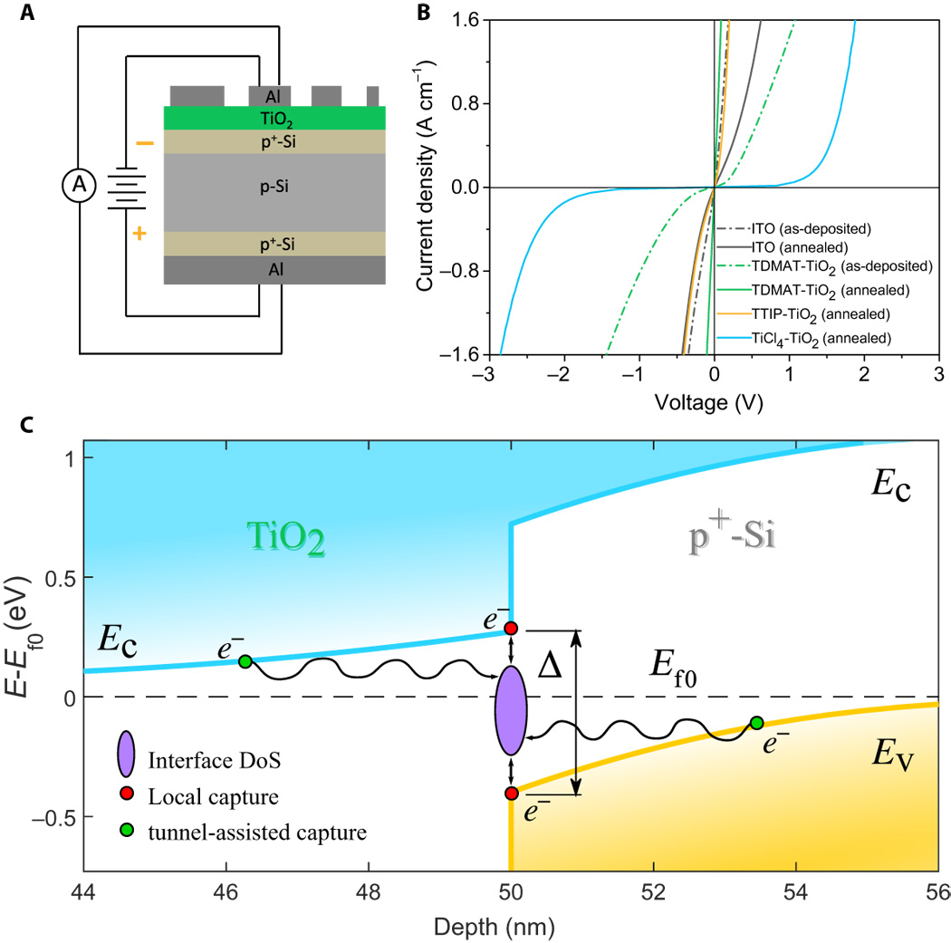
Contact behavior and simulated band diagram of TiO2/p+-Si interfaces. (A) Schematic of the structure used for measuring contact resistivity. (B) Comparison of the J-V behavior of ITO/p+-Si and various TiO2/p+-Si structures before and after annealing at 400°C in air. TiCl4-ALD TiO2 listed here is deposited with a reactor chamber temperature of 75°C. (C) Simulated band diagram of the TiO2/p+-Si at equilibrium assuming n-type doping of 5 × 1018 cm−3 on TiO2 and 1019 cm−3 for p+-Si (appropriate for our test structure with TDMAT TiO2; see table S3). The unknown interfacial energy gap Δ is shown here for illustrative purposes as 600 meV, which falls within the range of reported measurements (31). Both mechanisms of direct- and tunneling-assisted capture by interfacial density of states (DoS) are shown.

The Australian-Californian team conclude :
  • Successful demonstration of two proof-of-concept 2-T perovskite/Si tandem devices that function without a conventional interlayer between their subcells.
  • fabrication of an nc-Si tunnel junction interconnect is relatively straightforward for HIT cells, these layers introduce a small but potentially important amount of parasitic loss in the region of ~550 to 700 nm (16), where the nc-Si is absorbing and the perovskite top cell’s absorption is simultaneously incomplete.
  • The publication of a similar scheme using SnO2 (40) instead of TiO2 while this paper was under review demonstrates the wide applicability of the interlayer-free concept. Jointly, our work highlights the potential of emerging perovskite photovoltaics to enable low-cost, high-efficiency tandem devices through straightforward integration with commercially relevant and emerging Si solar cells.

Tuesday, January 8, 2019

Review form IEDM2018 - The World After Copper

Here is a very good review form IEDM2018 - The World After Copper by Paul McLellan

Thank you for sharing this one Henrik Pedersen! Indeed, Ru is coming!

IEDM: The World After Copper

I remember Gary Patton, the CTO of GLOBALFOUNDRIES, telling me once that research seemed to have flipped, and whereas he used to have most people working on transistors and interconnect was an afterthought, now it was the other way around. Just scaling the existing copper interconnect to get to the next generation was no longer enough.

At IEDM in December, there was a special session called Interconnects to Enable Continued Scaling. There were invited presentations by:
  • Arm and Georgia Tech
  • IBM
  • imec
  • UT Austin and GLOBALFOUNDRIES
  • Stanford
  • Applied Materials
Continue reading LINK 

LG Display’s 65-inch rollable OLED TV will go to production

ALD moisture barriers for flexible and shaped electronics, displays and solar cells have been researched, developed and scaled up for production for some time now. Besides rounded display edges of smart phones and gizmo's that have been shown at trade shows and other events there has not yet been that many potential high volume markets out there.
 
 
LG Display’s 65-inch rollable OLED TV as presented at CES2019 (youtube.com)
 
It’s been a year since LG Display’s 65-inch rollable TV prototype was demonstrated at CES, and now LG Electronics is bringing it to market as the company’s flagship 4K OLED TV for 2019. The finished Signature OLED TV R that consumers will be able to buy sometime this spring — for an astronomical, premium price — is quite similar to that prototype, but LG has refined the base station and added a 100-watt Dolby Atmos speaker for powerful built-in audio.This is a TV that’s there when you want it and disappears when you don’t. 
 
 
Youtube: LG Display’s 65-inch rollable OLED TV is only a prototype, so there’s no price or release date, but it’s still very cool. The Verge Senior editor Vlad Savov got a first look at the TV at CES 2018.
 
Not everyone loves having a big, black rectangle as the focal point of their living room, and plenty of people don’t own a TV at all. This TV disappears completely whenever you’re not watching. It drops slowly and very steadily into the base and, with the push of a button, will rise back up in 10 seconds or so. It all happens rather quietly, too.There’s also a mode — LG calls it “Line Mode” — where the display will drop down so that only about one-fourth of the panel is showing. You’ll still have on-screen music controls and the option to control your smart home gadgets in this mode. 
 
LG also includes some mood-setters like a crackling fireplace or rain sounds. Support for Alexa voice controls are being added this year in addition to the existing Google Assistant integration in LG’s webOS software; you just hold down the Prime Video button on the remote to bring up Alexa. And LG is also one of the companies that’s adding Apple’s AirPlay 2 for easy media playback or device mirroring. You can play music on the Atmos speaker system even when the TV is fully rolled up, which is great. Port selection is on par with other premium LG sets, and they’re all located at the back of the base. LG is making the move to HDMI 2.1 with its 2019 series, so that’s a big plus in terms of future proofing this very expensive TV.

Source: The Verge (LINK)

---------------------
By Abhishekkumar Thakur and Jonas Sundqvist

Monday, January 7, 2019

Picosun to showcase ALD for Medical applications at MDM West

ALD is steaming ahead into new fields and applications boyond the semiconductro industry. Meet Picosun at MDM West, the largest medtech event in North Americ.


Related Blog posts:

Nanexas PharmaShell® patent approved in the United States
Nanexa order a third Picosun ALD System to meet production demand for PharmaShell®
Picosun’s ALD nanolaminates extend the lifetime of biomedical microimplants
Picosun launches new PicoMEDICAL™ solutions specially targeted for healthcare industries
Groundbreaking micromedicine with Picosun’s ALD solutions

Versum Materials report 1,000 CHEMGUARD® GEN III Systems sold

[Versum Materials Newsletter, LINK] An important milestone for the Versum Materials DS&S was realized recently with the sale and commissioning of the onethousandth (1,000) CHEMGUARD® Gen III high-purity, liquid delivery system since its introduction in 2016. The 1,000-plus units are now running in the latest high-volume semiconductor fabs globally with more than 200 molecules now approved for delivery. Built on a legacy of more than 30 years of supplying advanced materials and delivery systems to the worldwide semiconductor and electronics industries, Versum Material’s DS&S team continues to design and build safer, more reliable delivery equipment for high-purity gas and liquid distribution.
 
 
CHEMGUARD 500 is specifically designed for very low vapor pressure precursors. The patented, automa􀆟c solvent purge ensures molecule purity on some of the lowest vapor pressure molecules used in semiconductor manufacturing. A small sample of the molecules approved in a CG500 are: TDMAT, TDEAT, TAETO, TBTDET, TDEAH, TEMAH, TEMAHf, TEMAZr and TPOSL. (From the CHEMGUARD GEN III 500 DATA SHEET)

“The CHEMGUARD Gen III system has been very well received by Versum Materials major customers, especially with its built-in redundancies,” said Jeff Chung, DS&S Asia Sales Manager.

Said David Eshelman, CHEMGUARD Product Manager, “The CHEMGUARD product family was introduced in 1999 under the Schumacher brand. Our customers’ original requests for improved safety and uptime helped to create the CHEMGUARD systems.”

Eshelman further explained that those requirements still exist today, but with each node, the molecules and processes used have become much more technically challenging. “The specific needs of today’s specialty, flammable or highly energetic molecules have been addressed by the unique CHEMGUARD Gen III model designs.”

Capitalizing on its materials and delivery systems expertise, Versum Materials recently created an experienced, multidisciplined team to review new molecules as they ramp and gain market acceptance. The team evaluates the molecule safety and process needs and helps speed the time-to-market for new molecules and processes by having a delivery solution ready when technology ramps.

“When our team says ‘Go,’ we know that a molecule is CHEMGUARD-ready,” said Eshelman. “The next node is right around the corner. We want the market to know that the established CHEMGUARD system continues to advance to meet the demands of a changing marketplace.”

CHEMGUARD GEN III CONTROLLER RETROFIT DATA SHEET (http://bit.ly/2PO164F)
CHEMGUARD GEN III 500 DATA SHEET (http://bit.ly/2zlnFU8)
CHEMGUARD GEN III 100 – 400 DATA SHEET (http://bit.ly/2QhjOBd)

Saturday, January 5, 2019

EuroCVD 22 & Baltic ALD 16 | 24-28 June 2019, Luxembourg Abstract submission deadline: 21 January 2019

The EuroCVD 22-Baltic ALD 16 Conference will take place in Luxembourg on 24-28 June 2019. The conference will offer a high quality scientific program with invited and contributed lectures in key development areas based on chemical processing from the gas phase.


The submission of contributions is open up to the 21st of January 2019.

Submit your abstract

Friday, January 4, 2019

Nanexas PharmaShell® patent approved in the United States

The US Patent Office has approved Nanexa's patent application for the PharmaShell® drug delivery platform.

Nanexa AB is a nanotechnology drug delivery company focusing on the development of PharmaShell®, which is a new and groundbreaking drug delivery system that is expected to have great potential in a number of medical indications. Within the framework of PharmaShell®, Nanexa has partnership agreements with among others, AstraZeneca.

The US Patent Office has approved Nanexa's patent application on January 1, 2019. The now-approved patent covers the product PharmaShell® as well as the method of its manufacture and formulation of PharmaShell® coated drugs. The approved patent has patent number US 10166198.

CEO David Westberg comments:

It is with great satisfaction that I can now conclude that the PharmaShell® patent is approved in the United States. We have always felt secure in our patent situation, but it still means a lot to get it confirmed by the US Patent Office. The US is our largest market and now that we have an approved patent, we can have a more interesting position in discussions with potential partners.

Source : Nanexa (in Swedish, LINK)

Nanexa order a third Picosun ALD System to meet production demand for PharmaShell®

[Picosun, LINK] ESPOO, Finland, 4th January 2019 – Picosun Group, a leading, global supplier of ALD (Atomic Layer Deposition) thin film coating technology, and Nanexa AB, a nanotechnology company focused on nano-enabled drug delivery solutions, solidify their collaboration in pharmaceutical ALD.


Picosun is now delivering their third ALD system to Nanexa’s facilities in Sweden, where it will be utilized in production expansion of nano-functionalized pharmaceuticals for drug delivery. Stock-listed Nanexa AB has two patents pending for their technology platform PharmaShell®. With this technology, ALD-functionalized pharmaceuticals can stay effective in the body for long periods of time and have a tailored release profile that minimizes side effects and eliminates the need for constant re-dosing. Picosun has been aiding Nanexa in their undertaking to develop their technology to an industrially mature state by supplying ALD tool solutions and consultancy.

Picosun provides various ALD solutions specially optimized to meet the needs of the medical industries where quality, reliability, efficiency, patient safety and minimized side effects are of utmost importance.

“We are very pleased to order our third PICOSUN™ ALD system. We have reached a point where the demand from our commercial partner to invest in our technology platform PharmaShell® is rapidly increasing. To be able to meet this demand we are now procuring a new ALD tool to extend our production capacity for efficient delivery of materials to our customers,” says David Westberg, CEO of Nanexa.

“We are happy to provide yet more PICOSUN™ ALD equipment to our long-time partner Nanexa, where our technology is used in manufacturing state-of-the-art medicines to combat some of the most difficult diseases. Our aim is to utilize ALD to enable solutions that benefit the whole humanity, which is why we are especially glad that healthcare industries are now seizing the potential of ALD on so many fronts,” continues Dr. Jani Kivioja, CTO of Picosun.

Thursday, January 3, 2019

Innovation and IP filing in Atomic Layer Deposition has moved from Memory to Logic

By studying the filing of IP world wide one can clearly see the trend how innovation in Atomic Layer Deposition (ALD) has moved from Memory to Logic. During the introduction of ALD (2003 to 2006) in high volume manufacturing of DRAM on 300 mm wafers most IP was filed by Samsung, Micron and SK Hynix. 10 years later (2013-2018) the IP filing lead has been taken over by Logic MPU manufacturers TSMC, Intel and Globalfoundries.

The patent application assignee from the past 25 years.

ASM International received a supplier excellence award from TSMC

[ASM International, LINK] ASM International N.V. (Euronext Amsterdam: ASM) has received a supplier excellence award as one of five equipment suppliers from TSMC for the performance and support of ASM's CVD equipment and technology during 2018. The award was presented to ASM by Dr. C.C. Wei, TSMC's Chief Executive Officer, at the TSMC Supply Chain Management Forum on December 6, 2018 in Taiwan.

The award was received by ASM in recognition of its CVD technology and performance in production at TSMC fabs. During the presentation, TSMC explained three points that contributed to the award to ASM.

1) Close engagement with TSMC and precursor suppliers to innovate process solutions.

2) Continued effort on cost and productivity improvement.

3) Exceptional manpower arrangement for delivery.


"We are very honored to receive this prestigious award from TSMC. On behalf of ASM, I would like to thank TSMC for this recognition," said Chuck del Prado, CEO and President of ASM International. "ASM strives to continuously advance our technology solutions and our partnership with TSMC is of strategic importance to ASM. We are very pleased that TSMC has benefited from the performance of our ALD and Epitaxy deposition tools in its production fabs."

TSMC is the world's largest semiconductor manufacturing foundry. TSMC holds the Supply Chain Management Forum annually to show appreciation for the support and contributions of their suppliers and to recognize outstanding equipment and materials suppliers.

Call Abstracts - Nano-Optics International School Feb 2019

Nano-Optics International School. Feb 2019. Call Abstracts. Early Bird Registration.

Venue: International Iberian Nanotechnology Laboratory (INL),Braga, Portugal

http://nano-optics-school-2019.org/


The 2nd Edition of IUVSTA NANO OPTICS School ha been organized to provide the rare opportunity to learn from and interact with some of the top experts in the field, both from academia and from companies. Ph.D. and master students are encouraged to attend the School and present their research work. Strong interaction between lecturers and students will be promoted during the entire school. Sessions on “Science Communication” and on “Project Management” oriented for students and young researchers are included in the programme. A guided visit to the INL laboratory http://inl.int/ is included in the programme.

COST Action MP1402 - HERALD
Hooking together European research in Atomic Layer Deposition

Wednesday, January 2, 2019

IEDM 2018 Imec on Interconnect Metals Beyond Copper

At IEDM in December 2018 Imec presented recent results from their interconnect program “Interconnect metals beyond copper – reliability challenges and opportunities”, which was recently covered by Scotten Jones (SemiWiki).
 

The electrical current in interconnect lines haven’t scaled down as fast as the lines' cross sectional area, which has enhanced the current density in the lines. Initial wide aluminum (Al) interconnects were first replaced by narrower aluminum-copper (AlCu) alloys and eventually by Cu to reduce the interconnects line resistance. Now even Cu needs to be replaced by alternate materials for the narrowest lines due to the following limits:

  • Higher resistivity with shrinking line width – below 20nm exponential increase in line resistance.
  • Via resistance also goes up strongly due to the liner.
  • Thinner lines see more grains from electroplating – around 10nm line can’t meet electromigration.
Imec commenced their work on alternative materials for M0 and M1 interconnects by screening based on the two metrics—resistivity multiplied by electron mean free path and melting point. The work reflects Rhodium and Iridium as the best candidate materials for the lowest interconnects that can be reasonably integrated. Ruthenium (Ru) and Cobalt (Co) exhibit similar performance. These materials can be deposited using ALD, CVD or electroplating. Co needs a thin adhesion layer but not a barrier layer. Ru also doesn’t require any seed or barrier layer. Imec is still working on reliability tests of these materials.

Meanwhile, TSMC has been using Co capping on Cu interconnects since 16 nm due to improved electromigration. Co (TSMC) and Ru (Intel) seed layers were introduced. Intel has introduced Co contacts at 10 nm and TSMC at 7 nm. Intel has also introduced Co interconnects for metals 0 and 1 at 10 nm.

Source: SemiWiki, Scotten Jones : LINK
 
----------
By Abhishekkumar Thakur

Sunday, December 30, 2018

Weebit Nano partners with Indian Institute of Technology Delhi on ReRAM Research

Resistive random access memory (ReRAM) and other emerging memory technologies have been getting a lot of attention in the past year as semiconductor companies look for ways to more efficiently deal with the requirements of artificial intelligence and neuromorphic computing. Neuromorphic applications are designed to specifically mimic how the human brain learns and processes information, and ReRAM devices show promise for enabling high-density and ultimately scaled neuromorphic architectures because they are significantly smaller and more energy-efficient than current AI data centers. They also mimic the brain’s biological computation at the neuron and synaptic level. 
 
 
Weebit Nano recently partnered with the Non-Volatile Memory Group of the Indian Institute of Technology Delhi (IITD) on a collaborative research project that will apply Weebit’s SiOx ReRAM technology to computer chips used for AI. 
 
Source: EETimes LINK
 
[RRAM-Info] Weebit Nano was established in Israel in 2014 with an aim to commercialize a Rice University's SiOx RRAM technology. The company aims to show a "commercially viable" product by the end of 2017. In August 2016 Weebit Nano performed a reverse-merger with an Australian miner to become a public company (ASK:WBT). In September 2018 Weebit raised $2.16 million USD via a share placement

----------
By Abhishekkumar Thakur, Jonas Sundqvist

Tuesday, December 25, 2018

Intel 10 nm Logic Process Analysis (Cannon Lake) by TechInsight

[TechInsight, LINK] TechInsights has found the long-awaited Cannon Lake - the Intel 10 nm logic process inside the i3-8121U CPU, used in the Lenovo IdeaPad330.

 
This innovation boasts the following:

  • Logic transistor density of 100.8 mega transistors per mm2, increasing 10nm density 2.7X over the 14nm node
  • Utilizes third generation FinFET technology
  • Minimum gate pitch of Intel’s 10 nm process shrinks from 70 nm to 54 nm
  • Minimum metal pitch shrinks from 52 nm to 36 nm
Process Highlights:

  • Deepest scaled pitches of current 10 nm and upcoming 7 nm technologies
  • First Co metallization and Ru usage in BEOL
  • New self-aligned patterning schemes at contact and BEOL
Design Highlights:

  • Hyperscaling via 6.2-Track high density library
  • Contact on active gate (COAG) cell-level usage
---------
By Abhishekkumar Thakur

Sunday, December 23, 2018

2.5 million euros for developing innovative electrolytic cell using ALD

2.5 million euros for developing innovative electrolytic cell 

EurekaAlert!, Public Release: 

Working together with external partners, chemists, materials scientists and chemical engineers at Friedrich-Alexander-Universität Erlangen-Nürnberg (FAU) have developed an innovative microcell for water electrolysis. They hope to replace standard plate electrodes used to split water into oxygen and hydrogen with compact, nanostructured tubes. They aim to simplify production, increase flexibility of use and avoid the need for expensive precious metals. A total of 2.5 million euros in funding has been earmarked for the 'Tubulyze' project which is due to start in early 2019 and is planned to run for four years.


Hydrogen is considered a promising means of saving and providing energy in an environmentally friendly and sustainable way. The element is available in virtually unlimited quantities in water molecules, but it is not easy to extract. Expensive and complex electrolysis procedures are needed to split water into oxygen and hydrogen. Mostly, large plate electrodes coated with catalysts are plunged into huge basins of water. In order to allow chemical electrolysis to take place under such highly corrosive conditions, catalysts made of expensive precious metals such as iridium and platinum are used. The membrane needed for ions to be exchanged between the anode and cathode is another costly factor.

Tube cell with ultra-thin catalyst layer

Engineers and chemists at FAU are now researching an electrolytic cell which avoids considerable disadvantages entailed by standard technology. Their idea: the cell takes the form of a tube, not a plate. At its core is an electrode made of porous titan, produced using a 3D printing process at the Chair of Materials Science and Technology of Metals (Prof. Dr. Carolin Körner). The surface of the electrode is then nanostructured and coated with an ultrathin catalyst layer - in this specific instance iridium - using atomic layer deposition. 'We can determine exactly how thick the coating layer should be, all the way down to the scale of an atom,' explains Prof. Dr. Julien Bachmann from the Chair of Chemistry of Thin Film Materials, who is responsible for coordinating the project. 'This allows us to work as cost-effectively as possible, as there is not a linear correlation between a thicker catalyst layer and increased current or greater output.'

Saturday, December 22, 2018

Quantum Dots-Silica Sphere with selective surface passivation by ALD for flexible displays

Bottom up Stabilization of CsPbBr3 Quantum Dots-Silica Sphere with Selective Surface Passivation via Atomic Layer Deposition
Qinyong Xiang, Binze Zhou, Kun Cao, Yanwei Wen, Yun Li, Zhaojie Wang, Chenchen Jiang, Bin Shan , and Rong Chen
Chem. Mater., 2018, 30 (23), pp 8486–8494

All-inorganic perovskite quantum dots suffer from poor stability in a humid and heat environment. In this article, CsPbBr3 quantum dots (CsPbBr3 QDs) are stabilized by coating nanoscale alumina on a CsPbBr3 QDs-silica luminescent sphere (CsPbBr3 QDs-SLS) via atomic layer deposition (ALD). Utilizing the intrinsic reactivity differences toward precursors, the surface defect sites of CsPbBr3 QDs are selectively passivated. The inorganic alumina coating layers can effectively reduce the ion migration and crystal deformation of CsPbBr3 QDs. In situ quartz crystal microbalance measurements show that organic ligands remain attached to the CsPbBr3 QDs surface during the ALD coating process. NMR, XPS, and first-principles calculations are performed to reveal the interaction strength between CsPbBr3 QDs-SLS and precursors. The surface passivation of alumina on CsPbBr3 QDs-SLS effectively stabilizes the QDs without reducing the photoluminescent quantum yield.


Reprinted with permission from Chem. Mater., 2018, 30 (23), pp 8486–8494. Copyright 2018 American Chemical Society.

Applied Materials showcases how Cobalt enables power and performance scaling at leading edge nodes


The semiconductor industry has already begun using cobalt to reduce contact and middle of line resistance. Replacing tungsten contacts with cobalt has paid dividends with an approximate 60 percent improvement in contact line resistance. Replacing the short-length copper interconnect at the lowest metal contact layers with cobalt has reduced via resistance (for lower IR drop) and improved electromigration reliability. 
 
New materials of interest include ruthenium and molybdenum, but both still lag cobalt from a maturity perspective. However, a detailed analysis of line resistance scaling shows that copper is superior or adequate to CDs of 12-15nm. Therefore, for metal levels above M1, where the interconnect is long enough for line resistance to be the key performance factor, copper wins. 
 
Integrating cobalt is not trivial, but Applied Materials has developed an “Integrated Materials Solution” for cobalt whereby the multiple process chambers needed to integrate cobalt can be combined into the same Endura platform, allowing wafers to be kept in vacuum for pristine materials engineering at ever more critical dimensions.

Applied Materials Blog: Cobalt Enables Power and Performance Scaling at Single-Digit Logic Nodes 

by Mehul Naik, Dec 17, 2018 (LINK)


 Logic CMOS scaling goals – performance, power, area and cost improvements. (Applied Materials)

---------
Written by Abhishekkumar Thakur

Friday, December 21, 2018

Area-selective ALD with high selectivity at TU Eindhoven

Here is a cool video for TU Eindhoven on Area-selective ALD with high selectivity just publishe in their AtomicLimits blog "Towards Area-Selective Atomic Layer Deposition with High Selectivity – Our perspective on area-selective ALD" by Adrie Mackus (LINK).


Picosun’s ALD nanolaminates extend the lifetime of biomedical microimplants

ESPOO, Finland, 21st December 2018 – Picosun Group, a leading, global supplier of ALD (Atomic Layer Deposition) thin film coating solutions, has developed a groundbreaking method for biocompatible encapsulation of microelectronic body implants.

Remote sensing and therapeutics through self-powered, wirelessly operating microimplants is an emerging technology that is finding a plethora of uses throughout the medical field. Some key examples are neural stimulation and diagnostics, blood glucose, blood pressure, intraocular and intracranial pressure measurements, and even artificial eyesight. These minuscule devices are typically implanted for extended periods of time (from several months to well over ten years), so encapsulation of their sensitive electronics against the corrosive environment inside the human body is crucial. Naturally, also the body has to be protected against possible inflammatory or rejection reaction caused by the implant. Traditional encapsulation materials, mostly used for macroscopic objects such as pacemakers or Cochlear devices, include titanium metal, ceramics, and several polymers such as parylene or polyimide. However, when the implant size diminishes, and the requirements for the implant lifetime increase, novel encapsulation methods and materials are called for. 

ALD is an ideal method for reliable, hermetic encapsulation of various implantable devices, from micro-scale sensors to more macroscopic items such as hip, knee, and dental implants. Several ALD materials are intrinsically biocompatible and inert in the human body. ALD method produces ultra-high quality thin films, that cover uniformly and conformally even complex 3D-structures with nanoscale details, thus the desired effect of the coating can be achieved with much thinner material layers compared to the traditional methods. ALD coatings can be applied at relatively low temperatures, which advocates their use also on sensitive materials such as plastics and polymers.

Picosun has now developed an ALD nanolaminate encapsulant that can potentially ensure microimplant lifetime of over 10 years in human body environment(*). The nanolaminate deposition process is readily scalable to high throughput, cost-efficient industrial production of hundreds or even thousands of implants per run in PICOSUN™ P-300B or P-1000 ultra-large batch ALD reactors.
 

Figure: SEM images showing conformal ALD nanolaminate on edges and corners of test Si pieces(*).

“There is an increasing number of customers in the healthcare industries that are now looking at ALD to solve some critical issues in their products. We at Picosun have developed a whole family of production-proven, turn-key PicoMEDICAL™ solutions specifically to answer this need. The excellent results of our ALD encapsulation for biomedical microimplants prove that our technological knowhow and decades of experience in the field are now paving the way for a whole new generation of ALD-enabled healthcare solutions,” says Dr. Jani Kivioja, CTO of Picosun Group.

Picosun provides the most advanced ALD thin film coating technology to enable the industrial leap into the future, with turn-key production solutions and unmatched expertise in the field. Today, PICOSUN™ ALD equipment are in daily manufacturing use in numerous major industries around the world. Picosun is based in Finland, with subsidiaries in Europe, North America, Singapore, Taiwan, China, and Japan, and a world-wide sales and support network. Visit www.picosun.com.

(*) J. Jeong, F. Laiwalla, J. Lee, R. Ritasalo, M. Pudas, L. Larson, V. Leung, and A. Nurmikko: Conformal Hermetic Sealing of Wireless Microelectronic Implantable Chiplets by Multilayered Atomic Layer Deposition (ALD), Adv. Funct. Mater. 2018, 1806440. DOI: 10.1002/adfm.201806440.

Chinese AMEC 5nm plasma etching tools verified by TSMC

DigiTimes report (LINK) that the Chinese OEM Advanced Micro-Fabrication Equipment (AMEC) announced recently its in-house developed 5nm plasma etching tools have been verified by Taiwan Semiconductor Manufacturing Company (TSMC). AMEC is already among TSMC's equipment suppliers for the foundry's 28nm, 10nm and 7nm processes.

Earlier in 2018 AMEC Introduced the Primo Nanova® System, which is the Company's first ICP etch Product for Chipmakers' most advanced memory and logic (LINK). Besides ICP AMEC has products based on CCP etch and platforms for TSV Etch (LINK).
 AMEC Introduced the Primo Nanova® System (AMEC)

Advanced Micro-Fabrication Equipment Inc. (AMEC)
AMEC is China's leading provider of advanced process technology to global manufacturers of semiconductors and solid-state lighting (SSL) products. Headquartered in Shanghai, the company is an entrenched supplier of dielectric and TSV Etch tools, helping chipmakers build devices at process nodes as low as 7nm. To date, nearly 800 AMEC process units have been positioned at 40 leading-edge semiconductor fabs across Asia. The company is also well established in Europe with AMEC MEMS tools running in production at major IDMs. In addition, with its MOCVD system, the company helps SSL manufacturers build today's most advanced LED products. To learn more about AMEC, please visit www.amec-inc.com.

Thursday, December 20, 2018

Hello China, Japan, Taiwan, Singapore and Korea - Please update the ALD Thesis list!

Please update the ALD history VPHA PhD thesis list on ALD PhD's. Currently, we're missing contributions from Asia. New contributions to be added here: LINK


Wednesday, December 19, 2018

Adrie Mackus at TU Eindhoven awarded NWO grants for development of sub 5nm ALE processing

Novel plasma processes for nanoelectronics

The fabrication of future sub-5-nanometer electronics requires etching with atomic level accuracy, which is beyond the reach of conventional plasma etching technology. In this project, novel plasma-based processes will be developed for layer-by-layer removal of material using atomic layer etching (ALEt). Adrie Mackus, leader of this project and Assistant Professor at the Plasma and Materials Processing group of Applied Physics, will collaborate with a diverse group of users from industry and academia, strengthening the leading position of the Netherlands in semiconductor equipment manufacturing.

Source: LINK

 
Nanolab@TU/e, a laboratory for nanotechnology research and innovation. Picture: Bart Van Overbeeke.
 

The semi equipment market will contract 2019 but grow 20.7 percent to reach an all-time high 2020

TOKYO – December 12, 2018 – Releasing its Year-End Total Equipment Forecast at the annual SEMICON Japan exposition, SEMI, the global industry association representing the electronics manufacturing supply chain, today reported that worldwide sales of new semiconductor manufacturing equipment are projected to increase 9.7 percent to $62.1 billion in 2018, exceeding the historic high of $56.6 billion set last year. The equipment market is expected to contract 4.0 percent in 2019 but grow 20.7 percent to reach $71.9 billion, an all-time high. [Source: SEMI LINK

For 2019, SEMI forecasts that South Korea, China, and Taiwan will remain the top three markets, with all three regions maintaining their relative rankings. Equipment sales in South Korea is forecast to reach $13.2 billion, in China $12.5 billion, and in Taiwan $11.81 billion. Japan, Taiwan and North America are the only regions expected to experience growth next year. The growth picture is much more optimistic in 2020, with all regional markets expected to increase in 2020, with the market increasing the most in Korea, followed by China, and Rest of World [Source: SEMI LINK]

After a period of record growth in 2017-18, the semiconductor equipment industry is expected to face a slowdown in 2019. Logic is strong but memory is weak, and the trade issues between the United States and China are a cause for concern. According to a report in Semiengineering (LINK), heading into 2019, there is a shortfall of 200 mm equipment. The industry requires from 2,000-3,000 new or refurbished 200 mm tools to meet fab demand, according to SurplusGlobal. But there are only 500 available 200 mm tools on the market, according to the company. 200 mm tool prices will remain high. 300 mm tool prices are lower than 200 mm tool prices these days
For the ALD OEM market the situation is therefore heating up even though the. Currently the top 300 mm ALD equipment companies (ASM, TEL, Lam, Jusung, Wonik IPS, Applied Materials) does not actively support the market with pure play 200 mm products except for Large Batch Furnaces. So if you want a 200 mm single wafer ALD tool today you can buy a 300 mm tool and equip it with 200 mm handling or go to one of the smaller companies like Picosun, Veeco, Beneq, Oxford Instruments, which all have 200 mm ALD cluster products on the market today.
From presentation "ALD/CVD applications, equipment and precursors in high volume manufacturing" at SEMICON Europa 2018, available on SlideShare LINK.
----
Written by Abhishekkumar Thakur and Jonas Sundqvist

Tuesday, December 18, 2018

The Chip History Center web site

Here you go - the best holiday web to explore for all of you LINK

Launched in September of 2004, The Chip History Center web site was originally developed by VLSI Research Inc to be the Semiconductor Industry’s History Channel on the Internet to help strengthen the industry’s infrastructure by providing an archive of videos and reports that document the industry’s history and its development. Today its purpose is to
  • Serve as a virtual museum on the history of the semiconductor industry
  • Preserve and archive the history of the industry that opened the doors to the information age
  • Provide easy-to-access and free information to researchers, historians, and educators
  • Provide educational resources for K-12 that show how things work
  • Provide role models to children about people for whose lives have been enriched by science and math

Early-Bird - The 4th-annual Critical Materials Council (CMC) Conference will be held April 25-26, 2019

Early-Bird Registration Now Open!
The 4th-annual Critical Materials Council (CMC) Conference will be held April 25-26, 2019 at the Saragota Hotel and Casino in Saratoga Springs, New York. The public conference follows the private CMC Fabs F2F meeting and Members Joint Session April 23-24, at GlobalFoundries in Malta (near Saratoga Springs).
 
"Materials for Advancing Processes & Technologies"
Keynote:
JOHN PELLERIN,Ph.D.,
Deputy CTO & VP of Worldwide R&D, GlobalFoundries  
 
Featured Presentations:
 
Dr. Karl Robinson, Director of Process Engineering, IMEC,  
"Materials Engineering in CMOS and Beyond-CMOS Applications"
 
G. Dan Hutcheson,
CEO, VLSI Research,
"Slowdown: When did it start? What drove it? and When will the recovery come?"

Three sessions will cover:  
 
I.  Global supply-chain issues of economics & regulations
II.  Immediate challenges of materials & manufacturing   
III.  Emerging materials in R&D and pilot fabrication    
 
Powerful & actionable presentations, and the popular Not-so-unusual Round Table Session - a highly differentiated program, with networking opportunities for all attendees.
 
Attendees will include industry experts handling supply-chains, business-development, R&D, and product management, as well as academics and analysts. CMC member companies will be attending this meeting, as it is an important part of their membership.  
Event Sponsorship Opportunities
Strengthen and Grow your Presence 

in the semiconductor industry. Use CMC Conference sponsorship as a pathway to leading semiconductor fabricators, OEMs, and materials suppliers. Sponsorships opportunities include virtual and in-person representation before, during and after the Conference, and may include active participation in our Not-So-Usual-Round-Table session. For more info go to https://cmcfabs/sponsorships/ or contact cmcinfo@techcet.com.

Standard Registration (after March 15) $495   

www.cmcfabs.org/cmc-events/

Monday, December 17, 2018

High Speed Batch Atomic Layer Deposition using Vortex ALD by Lotus Applied Technology

Here is a cool animation on the Lotus High Speed Batch Atomic Layer Deposition using Vortex ALD.


YouTube.com
 
Founded in 2007, Lotus Applied Technology was formed through a spinoff of the thin film process group within Planar Systems, Inc., a pioneer in Atomic Layer Deposition technology and manufacturing. Housed in a fully dedicated 20,000 square foot thin film processing and R&D facility in Hillsboro, Oregon, the team of technologists has been working together for over 20 years, developing innovative solutions to thin film processing challenges. Their equipment set includes a wide array of thin film deposition, lithography, and patterning equipment, including a versatile set of ALD equipment:
  • Six P400 Conventional Pulse-Based Batch ALD reactors
  • Roll to Roll ALD Research Scale Reactor
  • TransFlex Roll to Roll ALD Pilot Scale Reactor
  • Vortex Rotary Batch Reactor

Highly Sensitive ALD SnO2 Sensors and the Role of its Thickness in Gas Sensing Capabilities


Highly Sensitive ALD SnO2 Sensors and the Role of its Thickness in Gas Sensing Capabilities Published on Dec 4, 2018
 
Authors: Akhilesh Tanneeru, Zachary Taylor, Bongmook Lee, Veena Misra Abstract: 
 
We report superior gas sensing properties of nano-layered atomic layer deposited - tin oxide thin films with room temperature operation and discuss the role of thickness on the sensing response of the films. 25, 50, 100 cycles of tin oxide ALD films have been evaluated for response with ozone gas in the concentration range of 25ppb-100ppb. At 75ppb of ozone, relevant concentration indicated for an Asthma attack, a remarkable increase in sensitivity by 22 times is seen with the 50 cycles ALD SnO2 sensor over the 100 cycles sensor and an increase of 58 times, with the 25 cycles sensor over the 50 cycles sensor. The operating power per sensor was under 200uW including the power consumed by an UV LED (385nm wavelength) used for resetting the sensors’ baseline resistances. 


Saturday, December 15, 2018

Oxford Instruments participates in the EU Quantum Technology Flagship Programme (QMiCS)

[Oxford Instrument News] Oxford Instruments NanoScience is pleased to announce a partnership with the leading European institutions, including renowned research groups from Germany, France, Spain, Finland, and Portugal. The group is led by the Walther-Meißner-Institute (WMI) of the Bavarian Academy of Sciences and Humanities in Garching, Germany on a European project for developing new quantum applications. The collaborative consortium awarded a three million Euro grant from the EU Quantum Flagship Programme, for the proposal on ‘Quantum Microwaves for Communication and Sensing (QMiCS)’.

QMiCs project partners:
QMiCS aims at creating a technological basis for improving communication and sensing methods by employing dedicated micro- and nano-structured circuits, made from superconducting materials, cooled down close to absolute zero temperature to generate microwave radiation exhibiting a particular quantum mechanical property called ‘entanglement’. Exploiting entangled microwaves, a prototype quantum local area network cable for distributed quantum computing and a proof of concept for quantum-enhanced radar shall be demonstrated at WMI within the next three years. Oxford Instruments’ role will be to develop a cryogenic link between two ultra-low temperature fridges one provided by Oxford Instruments NanoScience and the other by the WMI to facilitate the microwave communication at very low temperatures. “We are excited at the potential of developing the next generation of quantum technology tools in association with such leading EU researchers in a consortium led by WMI to enable new innovative applications, using the company’s well established and diverse experience in superconducting and cryogen free ultra-low temperatures”, said Ziad Melhem, the Strategic Business Development Manager from Oxford Instruments NanoScience.

Wednesday, December 12, 2018

UNSW and Leadmicro announce a joint initiative to develop next generation high-efficiency solar cells

[Leadmicro News] The University of New-South Wales (UNSW) in Australia, and Jiangsu Leadmicro Nano-Equipment Technology Ltd. (LEADMICRO), a China-based global manufacturer of advanced thin film deposition and etch equipment, have announced a partnership to develop the next generation high-efficiency solar cells based on novel Atomic Layer Deposition (ALD) technology within the frame work of an Arena Project entitled “Advanced high-efficiency silicon solar cells employing innovative atomic scale engineered surface and contact passivation layers”. Mr Warwick Dawson, Director of Knowledge Exchange, Prof. Mark Hoffman, Dean of Faculty of Engineering, Prof. A/Prof Bram Hoex of School of Photovoltaic and Renewable Energy Engineering, as well as Mr. Yangqin Wang, Chairman of the LEAD Group and Dr. Wei-Min Li, CTO of LEADMICRO witnessed the signing ceremony.


Left to right: Research Fellow, Ouyang Zi; Chairman of Wuxi Lead Intelligent Equipment Co. Ltd., Mr. Yanqing Wang; CTO of Jiangsu Leadmicro Nano-Equipment Technology Ltd., Dr Wei-Min LI; Director Knowledge Exchange at UNSW, Warwick Dawson; Dean of Engineering at UNSW, Professor Mark Hoffman; Associate Professor Bram Hoex.

The photovoltaic industry is currently amid the transfer to the technologically superior PERC technology which was developed at UNSW in the late 1980s. According to A/Prof Bram Hoex, who leads the project at UNSW, “A major part of the advantages of the PERC solar cell compared to the incumbent technology is due to the application of ultrathin films which reduce the electronic losses at the non-contacted areas at the rear of the silicon solar cell. It is generally accepted that the next technological node will use so called “passivating contacts” which simultaneously allows for low electronic and resistive losses. These passivating contacts typically consist of a combination of ultrathin films, thus we see that nanoscale thin films will play an increasingly important role in solar cells. ALD allows controlling the growth of thin films at the atomic level and therefore is ideally suited for making these contacts.” In this project, Leadmicro will donate a pilot-scale ALD reactor to UNSW which will be housed at its Solar Industrial Research Facility (SIRF) at UNSW’s Kensington campus. “The fact that we will have a high-throughput reactor available on campus will allow us to very quickly transfer the processes we develop at the lab-scale tools and test their performance at the solar cell device level, so the technology is ready for Leadmicro’s clients to use in high-volume manufacturing” says A/Prof Hoex.

UNSW Dean of Engineering Prof. Mark Hoffman said: “UNSW leads the world in photovoltaic research and development, and I am very pleased that Leadmicro has chosen to partner with us. Together we will drive further efficiencies in solar cell technology. Collaborations such as this one between researchers and industry, where prototypes can be tested before being placed into full-scale production, are crucial to driving the economic benefits of discoveries. I am thankful to Leadmicro for their support and look forward to seeing the outcomes of this partnership,” Professor Hoffman said.

“Leadmicro’s proprietary ALD technology has become the mainstream choice for mass production of high-efficiency solar cells based on passivated contact technology, we are excited to partner with world leading solar energy research center at UNSW to spearhead the development of ALD technology for next generation silicon based solar cell manufacturing that’s above 25% conversion efficiency.” says Dr. Wei-Min Li, CTO at Leadmicro. “In the past two years Leadmicro has made significant contribution to global solar industry with world leading ALD technology that enabled higher efficiency with significant cost reduction. Leadmicro is an example of new trend of Chinese company that is strived for technology innovation and localization. I’m happy to see the collaboration between Leadmicro and world leading research organization at UNSW to pioneer the new technology for high-efficiency solar cells production and contribute further to our noble endeavour of renewable energy for a clean world.” Says Mr Yang Qin Wang, Chairman of the Lead Group.

About UNSW

The University of New South Wales (UNSW) is an Australian public research university located in the Sydney suburb of Kensington. Established in 1949, it is ranked 4th in Australia, 45th in the world, and 2nd in New South Wales according to the 2018 QS World University Rankings. UNSW has been a world-leader in the field of photovoltaics for over four decades.

About LEADMICRO

Jiangsu Leadmicro Nano-Equipment Technology Ltd is a global equipment manufacturer specialized in development, design, manufacturing, and services of the advanced thin film deposition and etch equipments for industrial production applications. Leadmicro’s business areas cover a wide range of industries including new energy, flexible electronics, semiconductor, and nano-technology.