Wednesday, August 23, 2023

Silicon Carbide Empowers Power Semiconductors in Thriving Industry Transition

A paradigm shift is sweeping the power semiconductor landscape, with silicon carbide (SiC) emerging as the frontrunner. Driven by EV adoption and cost parity with silicon, SiC's ascendancy is reshaping the market. Thousands of SiC-based power semiconductor modules are already enhancing EV functions such as charging and conversion. SiC MOSFETs are supplanting silicon-based IGBTs, doubling power density and ramping switching speeds while downsizing form factors. This transformation hinges on SiC modules achieving price parity with silicon alternatives, fostering supply alliances and new SiC fabs. SiC modules play a pivotal role in the transition to 800V batteries, boosting EV adoption through faster charging and reduced costs. Despite challenges, analysts anticipate substantial SiC growth, particularly in automotive applications. This evolutionary journey towards energy-efficient power is projected to culminate in a $6.3 billion SiC power semiconductor market by 2027. 

In the pursuit of advancing silicon carbide (SiC) technology, a suite of innovative wafer process tools is being employed. These tools encompass high-temperature epitaxial growth exceeding 2,000°C, hot ion implantation, rapid thermal processing (RTP), and Atomic Layer Deposition (ALD). Noteworthy adaptations are underway in wafer grinding, chemical-mechanical polishing (CMP), as well as the formulation of abrasion-resistant polishing pads and slurries tailored for the rigid, fragile SiC substrate. The evolution also encompasses novel materials like strippers and cleaning formulations, addressing device requirements and sustainability considerations. These cutting-edge processes collectively exemplify the industry's determination to optimize SiC production, enhance its characteristics, and foster its integration into diverse applications, from electric vehicles to renewable energy systems.

Power Semis Usher In The Silicon Carbide Era (semiengineering.com)

Tuesday, August 22, 2023

Beneq invites you to ALD TechDay during SEMICON Europa 2023

Beneq invites you to ALD TechDay during SEMICON Europa 2023 in Munich this November! Discover the latest trends and applications in Atomic Layer Deposition (ALD) for specialty semiconductors. Industry leaders and experts will share insights on ALD adoption and its impact.

Don't miss this exclusive forum brought to you by SEMI and Beneq. Register now!


ASM International Unveils Cutting-Edge Training Center in Tainan, Taiwan

Dutch semiconductor equipment leader ASM International NV has established a pioneering training center at the Southern Taiwan Science Park's Tainan branch to offer intensive training for over 100 engineers employed by its clients. This newly inaugurated facility is ASM's first training center in Taiwan and signifies a significant step in enhancing semiconductor expertise. With more than 50 percent global market share in atomic layer deposition (ALD), ASM's training center introduction aims to harness virtual reality technology for hands-on learning and precision semiconductor equipment mastery. The center is poised to propel innovation and foster synergies between Taiwan and the Netherlands, two pivotal players in the semiconductor industry.


The training center will leverage cutting-edge virtual reality technologies, allowing trainees to transcend conventional learning boundaries. The utilization of online courses coupled with virtual reality tools will empower engineers to grasp the intricate aspects of precision semiconductor equipment more effectively.

Guido Tielman, head of the Netherlands Office Taipei, highlighted the strategic collaboration between the Netherlands and Taiwan in shaping the global semiconductor landscape. He underscored the significance of this training center in fortifying ties and harnessing the immense business opportunities presented by the dynamic semiconductor sector.

This venture aligns with Taiwan's thriving semiconductor ecosystem, further enriched by the presence of other industry giants like ASML Holding NV, renowned for its extreme ultraviolet lithography (EUV) photolithography machines. The Netherlands, Taiwan, and ASM International are collectively poised to leverage their expertise to excel in the competitive global semiconductor market.

ASM International's state-of-the-art training center marks a pivotal moment in the advancement of semiconductor knowledge and technology. This strategic collaboration between the Netherlands and Taiwan is set to drive innovation, propel semiconductor advancements, and foster the development of highly skilled engineers, amplifying the capabilities of the global semiconductor industry.

Dutch IC equipment supplier opens training center in Tainan - Focus Taiwan

Nanexa's Breakthrough: Lenalidomide Controlled Release Confirmed in Phase 1 Study

Nanexa AB, a pioneering pharmaceutical company, has unveiled a significant advancement in the realm of drug delivery. The company recently revealed exciting results from its Phase 1 study, designated NEX-20-01, which underscored the controlled release of lenalidomide in varying doses over a span of up to 21 days.

Atomic Layer Deposition (ALD) is a cutting-edge technique used in medical and pharmaceutical applications, particularly in the development of Nanexa's PharmaShell® technology. ALD's precision in depositing thin layers of materials plays a vital role in creating the controlled-release shell of PharmaShell®. This nanoscale engineering ensures accurate drug delivery, regulating release rates and optimizing therapeutic effects. PharmaShell® benefits from ALD's versatility, enhancing drug efficacy, minimizing side effects, and allowing tailored treatment plans. ALD's role in crafting PharmaShell® exemplifies its impact in advancing drug delivery systems, revolutionizing pharmaceutical care.


The study, conducted with great precision and care, involved nine healthy volunteers who were administered either one or two subcutaneous single injections of the innovative NEX-20A formulation. This formulation encompassed doses ranging from 15 to 35 mg of lenalidomide, with a maximum cumulative dosage of 50 mg. The outcome was nothing short of remarkable, as the observed pharmacokinetic data from the human participants correlated excellently with the projected exposure calculated from preclinical studies.

Central to the accomplishment was the remarkable release mechanism employed by Nanexa, known as PharmaShell®. This ingenious approach ensured a controlled and gradual release of the drug into the participants' bodies, creating a plasma curve that spanned an impressive 21 days. A critical observation from the study was the initial low release of the total dosage within the first day. This gradual release strategy plays a pivotal role in maintaining optimal levels of the drug in the bloodstream throughout the treatment period.

Equally encouraging was the confirmation that the total exposure of lenalidomide in the plasma—measured as the area under the curve (AUC)—escalated proportionally with the administered dose. This finding aligns with the expectations and demonstrates the efficacy of the PharmaShell® system in achieving the desired therapeutic outcomes.

Nanexa's CEO, David Westberg, expressed his enthusiasm regarding this groundbreaking achievement. "This is an important achievement for Nanexa, to once again demonstrate that we can predict the release profile of PharmaShell® in humans based on preclinical data," he shared. Westberg also revealed the company's forward-looking plans, stating, "We are now continuing to optimize the formulation and are ready to plan for the next clinical study of NEX-20 in patients. In that study, where we plan to increase the dose, we want to ensure that we will continue to minimize local reactions, and we see good results from preclinical studies on how this can be done."

Safety, of course, remains a top priority in such endeavors. Nanexa is committed to compiling comprehensive safety and tolerability data, which will be meticulously assessed following the final follow-up visits for the last dose group in October. Encouragingly, the study thus far has reported limited and transient injection site reactions, with no unexpected severe or systemic side effects. This bodes well for the continued development and progress of the NEX-20 project.

Nanexa's accomplishments in the controlled release of lenalidomide mark a significant milestone not only for the company but also for the entire field of pharmaceuticals. The ability to meticulously regulate the release profile of drugs while simultaneously minimizing undesirable side effects holds great promise for revolutionizing patient care and treatment outcomes. As Nanexa continues to pave the way with its innovative approach, the future of pharmaceuticals looks more promising than ever.

Nanexa AB - Nanexa obtains pharmacokinetic data from the NEX-20 Phase 1 study confirming controlled release of lenalidomide

Immersive Collaboration: Imitera and AlixLabs Join Forces to Transform Semiconductor Manufacturing

In a groundbreaking partnership, Extended Reality (XR) technology leader Imitera and semiconductor innovator AlixLabs are set to reshape the way industries collaborate and innovate. The collaboration aims to leverage the power of XR to enhance visualization and communication within AlixLabs' semiconductor manufacturing process.

Revolutionizing Collaboration with XR

Imitera's cutting-edge XR platform is poised to unlock a new era of collaboration for AlixLabs. By creating a virtual environment where teams can interact with atomic and molecular structures, XR technology enables live testing and seamless sharing of information. This revolutionary approach empowers teams to make decisions collaboratively, irrespective of geographical barriers.


From Virtual Atoms to Real Insights

Dr. Jonas Sundqvist, CEO of AlixLabs, expressed his amazement at the insights gained through the XR atomic level world. He likened the experience to being immersed in an IKEA ball bath as he and his team explored atomic-level structures virtually. The technology not only sparks imagination but also provides real-world benefits for dispersed teams, like AlixLabs', to engage as if they were physically present.

XR Paving the Way for Industry Innovation

The collaboration between Imitera and AlixLabs exemplifies the transformative potential of XR technology. By addressing the demand for immersive, cost-effective, and user-friendly experiences, Imitera's XR solutions have the power to drive innovation across various industries. AlixLabs' groundbreaking semiconductor manufacturing technique coupled with Imitera's XR platform showcases a new way forward for industries to connect, visualize, and innovate.

Looking Ahead

The partnership between Imitera and AlixLabs isn't just about merging technologies; it's about merging minds. With XR technology as the bridge, teams can transcend traditional barriers and engage in a shared space that fosters creativity and informed decision-making. This collaboration marks a significant step toward revolutionizing industries and shaping the future of collaboration.

In a world where physical distances are no longer limitations, the synergy between XR and semiconductor innovation is a testament to human ingenuity. As these two worlds converge, the possibilities for cross-industry collaboration and discovery are boundless.

Imitera and AlixLabs Collaborate Using Cutting-Edge XR Solution to Revolutionize the Visualization of Atomic Level Semiconductor Manufacturing - AlixLabs AB (cision.com)

Indo-Pacific Region's Pivotal Role in Global Semiconductor Industry Supply Chain

Mapping the Semiconductor Supply Chain: The Critical Role of the Indo-Pacific Region

The report underscores the Indo-Pacific region's paramount role in the complex global semiconductor supply chain. Across various stages, from design to fabrication, the report illuminates the region's indispensable contributions to the industry's functionality and the wider impact on global economics and geopolitics.

The report highlights semiconductors' critical position in the world economy, impacting sectors like electronics and infrastructure. With annual sales surpassing half a trillion dollars and a far-reaching economic impact, recent events like the semiconductor shortage, causing a $240 billion GDP reduction and halting auto production, underscore this centrality.

The analysis delves into the intricate facets of the semiconductor supply chain, spotlighting the collective influence of Taiwan, Japan, China, and South Korea. These Indo-Pacific nations specialize in semiconductor design, fabrication, and more, with the United States as a significant player, reflecting its Pacific power status and industry leadership.

The authors unravel the complexities of design, fabrication equipment, materials, and assembly. They emphasize the U.S.'s lead in design software and intellectual property. The report also uncovers the Indo-Pacific's domination of manufacturing equipment, especially by the U.S., Japan, and South Korea.

Geopolitically, the report discusses how national strategies adapt to ensure resilient supply chains and technological sovereignty. It underscores the need for collaboration, particularly in the Indo-Pacific, to build robust ecosystems that counter risks and ensure secure supply chains.

Materials and Chemicals: Cornerstones of Semiconductor Manufacturing

The semiconductor industry's core relies on vital raw and manufactured materials like silicon wafers, photomasks, and photoresists, as well as crucial chemicals in the manufacturing process. The market for these fabrication materials exceeded $40 billion in 2021, concentrated mainly in the United States, Germany, Japan, Taiwan, South Korea, and China. Taiwan claimed the largest share with 25%, while Europe and China had smaller shares. Silicon wafers, forming a significant portion of the market, are essential components for semiconductor production. Their market has evolved over two decades, with five companies now controlling 95% compared to over 20 in 1990. 


Key players in silicon wafer manufacturing include Japanese, Taiwanese, German, South Korean, and French firms. While China's presence is growing, its ability to produce 300 mm/12-inch silicon wafers remains limited. Photomasks and photoresists, integral to semiconductor fabrication, are mainly dominated by Japanese, Taiwanese, and South Korean companies. China's progress in these areas has been notable, marked by investments aimed at enhancing their capabilities. The report highlights these materials' significance within the complex semiconductor supply chain and underscores the Indo-Pacific's pivotal role in their production and distribution.

Semiconductor Manufacturing Equipment: Key Players and Indo-Pacific Dominance

Summary: The semiconductor manufacturing process relies on highly specialized equipment to create intricate integrated circuits on silicon wafers. The Indo-Pacific region dominates the semiconductor manufacturing equipment (SME) market, contributing to 77% of global SME sales. The United States and Japan lead in SME production, with South Korea also playing a significant role. The United States and Japan excel in producing wafer fabrication equipment, while Japan has a strong presence in assembly and test equipment. 

China is a major player in assembly, test, and packaging (ATP) equipment, particularly through companies like ASM Pacific. The Indo-Pacific region is home to the majority of semiconductor fabrication facilities, with China rapidly expanding its fabrication capabilities. Additionally, ATP facilities are concentrated in the Indo-Pacific region, with Taiwan, China, and Southeast Asia (including countries like Singapore, Malaysia, Vietnam, and the Philippines) being key contributors. ATP facilities encompass processes such as chip cutting, testing, and assembling, and while these processes may be less complex compared to other stages of manufacturing, they have become more intricate with the continual shrinking of transistor size and density in semiconductor chips.

In summary, the report unveils the Indo-Pacific's pivotal role in the global semiconductor industry. By dissecting the supply chain and revealing its geopolitical implications, the report serves as a vital resource for policymakers and industry stakeholders in navigating this dynamic landscape.

Tokyo Electron's Q1 2024 Earnings Call Unveils Resilient Performance and Strategic Focus

Tokyo Electron Limited (OTCPK: TOELF), a prominent semiconductor equipment manufacturer, recently held its Q1 2024 Earnings Conference Call, revealing a resilient financial performance and strategic initiatives. Key representatives including Toshiki Kawai (CEO) and Hiroshi Kawamoto (Finance Division GM) presented the company's consolidated financial summary and insights into the business environment.

Financial Highlights:
- Q1 2024 sales reached ¥391.7 billion, showing a 29.8% decline due to reduced customer WFE spending.
- Gross profit at ¥162.3 billion and operating income at ¥82.4 billion represented drops of 35.5% and 46.0% from the prior quarter, respectively.
- Tokyo Electron invested in R&D, allocating ¥43.6 billion, while capital expenditures amounted to ¥39.3 billion, reflecting its commitment to innovation and expansion.

Market Outlook:
- Tokyo Electron discussed the WFE market's projected growth to $200 billion within 2024-2025.
- The company foresees opportunities in server, leading-edge CPU, DRAM, NAND, GPU for AI, HBM, power semiconductors for EV, and more.

Fiscal 2024 Estimates:
- Financial estimates remain unchanged, with ¥580 billion and ¥690 billion projected for the first and second halves of FY 2024, respectively, in SPE new equipment sales.
- Tokyo Electron aims for record-high R&D investment of ¥200 billion and CapEx of ¥124 billion to align with growth projections.

Share Repurchase and Dividend:
- Tokyo Electron's ongoing share repurchase program bought 3,069,200 shares worth ¥60.9 billion by July 31.
- The company plans to continue repurchase up to ¥120 billion by December 31, 2023.
- A consistent dividend forecast maintains a full-year dividend per share of ¥320.

Tokyo Electron's Q1 2024 Earnings Call provided a comprehensive overview of its robust performance and strategic direction, positioning the company to capitalize on growth opportunities in the semiconductor sector.


ALD Reactor Evolution: Tracing Milestones from Suntola to Today's Technological Landscape


The short but impactful 50-year history of Atomic Layer Deposition (ALD) has been a subject of extensive research and documentation, particularly in recent years. Examining the technology's evolution through an equipment perspective reveals the crucial role played by innovative equipment design in shaping the ALD ecosystem we have today. This ALDeep Dive episode embarks on a journey through the evolution of ALD reactors, highlighting key milestones and developments.


Episode Highlights:

**00:00 - Intro:** An introduction to the ALD technology and its rapid development over the past 50 years.

**01:33 - Suntola’s 1st Reactor:** Delving into Tuomo Suntola's original ALD reactor and its significance in kickstarting the technology's journey.

**03:15 - Suntola’s Patented Configurations:** Exploring the patented configurations of ALD reactors, including the technological advancements they brought about.

**07:38 - The First Commercial Reactor:** Reflecting on the emergence of the first commercial ALD reactor and its role in driving the technology towards industrial applications.

**10:50 - Plasma, Please:** Examining the introduction of plasma into ALD reactors and how it enhanced film deposition processes.

**15:20 - Powder ALD Reactors:** Investigating the utilization of powder-based ALD reactors, which added a new dimension to thin film deposition.

**20:37 - Reintroduction of Spatial ALD:** Discussing the reintroduction of spatial ALD and its implications for achieving precise and uniform coatings.

**24:10 - Today’s ALD Tool Landscape:** Taking a look at the current landscape of ALD tools, showcasing the advancements and variety available today.

**25:43 - Concluding Thoughts:** Summing up the journey through ALD reactor evolution and emphasizing the integral role of equipment innovation in ALD's remarkable growth.

**Key Papers & Patents:**

- "Chemical Vapor Deposition," 2014, 20, 10-11-12, 332-344

- T. Suntola, J. Antson, International patent, FIN 52359, US 4 058 430

- T. Suntola, A. Pakkala, S. Lindfors, International patent, FIN 57975, US 4 413 022

- "Journal of Vacuum Science & Technology A," Vol.29, No.5, Sep/Oct 2011

- "Journal of Vacuum Science & Technology A" 25 (5) Sep/Oct 2007

- "Applied Physics Letters" 92, 192101 (2008)

- "Journal of Vacuum Science & Technology A" 30, 021502 (2012)


This insightful ALDeep Dive episode traces the evolutionary path of ALD reactors, acknowledging their critical contribution to the ALD technology we know today. From Suntola's pioneering work to the latest advancements, the journey reveals the interconnectedness of equipment innovation and ALD's remarkable progress.

Applied Materials Surges on Impressive Q3 Earnings and Bullish Guidance

Applied Materials Inc. (NASDAQ: AMAT) witnessed a robust surge of nearly 4% in after-hours trading following the release of its third-quarter financial results that significantly outperformed expectations. The semiconductor capital equipment manufacturer reported adjusted earnings of $1.90 per share on $6.43 billion in revenue for the quarter ending July 30. 

Notably, the company's strategic focus on foundry and logic revenue paid off, accounting for 79% of quarterly sales compared to 66% in the prior year's quarter. Additionally, Applied Materials generated a substantial $2.58 billion in cash from operations during this period. The company's bullish performance extended to its outlook, with fourth-quarter net sales projected at approximately $6.51 billion, accompanied by adjusted earnings per share ranging from $1.82 to $2.18. These figures comfortably exceeded analyst estimates, highlighting Applied Materials' robust position in the semiconductor industry.


Applied Materials, Inc. (AMAT) Q3 2023 Earnings Call TranscriptSA TranscriptsThu, Aug. 17

Applied Materials, Inc. 2023 Q3 - Results - Earnings Call PresentationSA TranscriptsThu, Aug. 17

TSMC's 2nm Chip Plant Faces Delays in Taichung, Water and Electricity Hurdles Cited

Taiwan Semiconductor Manufacturing Company (TSMC) is experiencing setbacks in the construction of its highly anticipated 2-nanometer chip manufacturing plant in Taichung City, Taiwan. Delays have been attributed to challenges related to water and electricity supply, crucial for the resource-intensive chip fabrication process. This development comes as TSMC seeks to expand its manufacturing capabilities amid a rapidly evolving semiconductor landscape.

aiwan Semiconductor Manufacturing Company (TSMC), a global leader in semiconductor manufacturing, is facing delays in the construction of its planned 2-nanometer chip manufacturing plant in Taichung City, Taiwan. The director of the agency responsible for managing science and technology infrastructure on the island has indicated that the construction will not commence by the end of this year.

TSMC initially intended to establish two 2-nanometer manufacturing sites in Taiwan, with the first site in Hsinchu City. However, due to delays in the approval process for the Taichung site, the company confirmed its decision to also manufacture next-generation chips in Kaohsiung City.

The primary challenges affecting the Taichung site relate to the plant's water and electricity requirements. Chip fabrication demands high-purity conditions, necessitating large volumes of pure water to meet product purity standards. TSMC has encountered obstacles in securing an adequate water supply, particularly during a 2021 drought that led the company to employ water tankers to fulfill its water needs.

These developments underscore the intricate logistical challenges inherent in semiconductor manufacturing, where resource-intensive processes require precise environmental conditions. While TSMC continues to innovate and expand its global operations, addressing these challenges becomes paramount to maintaining its position at the forefront of the semiconductor industry.

ASM International N.V. has completed the purchase of a strategic plot of land in Scottsdale, Arizona.

ASM International N.V. has completed the purchase of a strategic plot of land in Scottsdale, Arizona. This move is a significant step towards consolidating ASM's multiple sites in Arizona, positioning the company for streamlined operations and future expansion in R&D and support activities.

The decision aligns perfectly with ASM's Growth through Innovation strategy, reflecting the company's commitment to adapting and evolving in the dynamic semiconductor landscape. While specific financial details remain undisclosed, this investment contributes to ASM's targeted €150-200 million total group capex for 2023, as communicated earlier this year.

ASM International N.V., headquartered in Almere, the Netherlands, is a key player in semiconductor equipment and process solutions. With facilities spanning across the United States, Europe, and Asia, ASM International is driving innovation and growth in the industry.

For more insights, visit ASM's official website: www.asm.com

Monday, July 17, 2023

Oxford Instruments Reveals Advanced ALD Research System for Quantum Applications

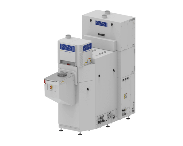
Oxford Instruments, a UK-based company, has introduced the PlasmaPro ASP, a breakthrough addition to the Atomfab product line, set to redefine atomic layer deposition (ALD) research. The system features an exclusive remote-plasma source design, optimized chamber geometry, and wafer stage bias, resulting in a remarkable threefold increase in ALD deposition rates—a milestone for research efficiency.
“We have experienced high pre-launch interest from the market for the PlasmaPro ASP for superconducting quantum materials. The PlasmaPro ASP is designed to address key quantum challenges with an innovative high-rate source design and high machine up-time, as well as an intuitive software user interface called PTIQ."

“With the source design derived from our Atomfab® ALD production product, the PlasmaPro ASP retains process speed and robustness, with the inclusion of additional hardware to increase flexibility, which offers a unique solution to the quantum market to speed up development cycles.” Dr Russ Renzas, Quantum Technologies Market Manager, Oxford Instruments Plasma Technology, Americas.

The collaboration with Eindhoven University of Technology (TU/e) on the plasma source design yielded accolades, with their joint research paper receiving recognition at the American Vacuum Society’s 22nd International Conference on Atomic Layer Deposition (AVS ALD/ALE 2022) conference.


With a primary focus on quantum technology, the PlasmaPro ASP facilitates the creation of essential low-resistivity and high-Tc superconducting nitride films. The system's intuitive software interface, PTIQ, along with its adaptable source design from Oxford Instruments' Atomfab ALD production product, ensures both rapid processing and robustness.

Anticipation for the PlasmaPro ASP's launch, especially for its potential in superconducting quantum materials, underscores the imminent impact of this innovation. Collaborative efforts with TU/e will likely accelerate advancements in quantum technology and various applications like electronics and photonics.

Professor Erwin Kessels of TU/e praises the PlasmaPro ASP for its distinctive capabilities, set to invigorate diverse research and innovation prospects.

Breakthrough Ultra-fast ALD Product - Oxford Instruments (oxinst.com)

Thursday, July 13, 2023

2023 Semiconductor Materials Market Slowing but Resilient

Material growth to resume in 2024 as industry recovers and fabs ramp up

San Diego, CA, July 12, 2023: TECHCET—the electronic materials advisory firm providing business and technology information— announced that the Total Semiconductor Materials market will contract by at least -3% in 2023 given the industry wide slowdown and reported higher levels of inventory in the materials supply chain. This year’s decline will result in revenues for Semiconductor Materials to total US$69.6 billion, down from the US$71.7 reported in 2022. However, leading-edge logic and automotive/power device production will limit the overall decline in materials revenues for 2023.
TECHCET is forecasting a strong recovery in the market in 2024, with total material revenues increasing 8% to almost US$75 billion. CAGR growth over the next 5 years is forecasted to be 4%, which will result in the market reaching US$88 billion by 2027.


To read the full article, go to: https://lnkd.in/gVan5qSq

To find out more: see TECHCET at SEMICON West at NY CREATES Booth (North Hall 5845) from July 11-13. Lita Shon-Roy, Diane Scott, Dan Tracy, and Kevin McLaughlin will all be there to share market insights and industry updates. Or visit our website here: https://lnkd.in/gJQ2Gt36.

Segment summarized by TECHCET previous recent releases:

Semiconductor Metal Plating Chemicals:

The market for semiconductor metal plating chemicals is expected to experience a slight decrease of 2% in 2023. This decline is due to lower expectations for overall wafer starts and inventory corrections within the market. Copper is the largest revenue contributor in this segment, particularly in advanced packaging wiring and interconnect copper plating. However, the market is expected to rebound in the long term, with a positive compound annual growth rate (CAGR) of 3.7% for advanced packaging and 3.3% for interconnect metal chemicals.

Semiconductor Quartz Equipment Components:

After reaching an all-time high in 2022, the market for fabricated quartz equipment components is expected to decline in 2023. The slowdown is attributed to a shift in industry investments and reduced purchase orders. However, the market is buoyed by previous purchases and backlogs, leading to a projected decline of 6% in 2023. New fab expansions are expected to drive future growth, with a CAGR of 5% from 2022 to 2027.

CMP Consumables:

Following strong performance in 2022, the CMP consumables market is forecasted to experience a slight reduction of 2.4% in 2023. The decrease is primarily due to oversupply in DRAM and market corrections. However, the market is expected to achieve a 5-year CAGR of 5.2%. The demand for new metals pads and slurry is anticipated to drive growth in this segment, particularly with the development of advanced logic methodologies and the evaluation of new BEOL materials.

Electronic Gases:

The electronic gases market is expected to witness a positive 5-year CAGR of 6.4% driven by expansions within the semiconductor industry, especially in leading-edge logic and 3DNAND applications. However, supply constraints for critical gases like B2H6 and WF6 may arise as demand outpaces supply. Disruptions in gas supply from current sources and geopolitical events may lead to shortages. Helium supply is also considered at high risk. Despite these challenges, the market is projected to grow, particularly with new fab expansions and increasing demand.

Semiconductor Wet Chemicals:

Semiconductor wet chemical revenues are forecasted to decline by 2% in 2023, following the trends in wafer starts and rising energy prices. The industry slowdown and instability from the Russia-Ukraine war contribute to the market contraction. However, the market is expected to rebound in 2024, with a 5-year CAGR of 3.9%. Phosphoric acid is the strongest segment within wet chemicals due to growth in the 3DNAND market. A holistic approach to the chemical supply chain is crucial for success in this market.

ALD/CVD Precursors:

The market for ALD/CVD precursors experienced a flattening in 2023 due to reduced memory pricing in production. However, a rebound is expected in the second half of the year, driven by the recovery of memory pricing. The market for high-ƙ and low-ƙ dielectric precursors is projected to rebound significantly in 2027, with a growth rate of approximately 19%. The market will be boosted by fab expansions, logic advancements, and increasing demand for metal and dielectric precursors.

Friday, June 30, 2023

Intel Takes Strategic Steps to Regain Semiconductor Chip Leadership

Intel plans to separate its manufacturing and fabless units to regain its semiconductor chip leadership. The move aims to serve emerging markets and make chip manufacturing more efficient. Intel seeks to emulate TSMC's success and become the second-largest external foundry by 2030.

In an effort to reclaim its position as a leader in the semiconductor chip industry, Intel has announced plans to separate its manufacturing and fabless units. This strategic move aims to address evolving market dynamics and capitalize on emerging sectors such as cloud computing, edge computing, and artificial intelligence (AI). By granting independence to its foundry business and diversifying its chip production, Intel aims to regain its competitive edge and accelerate chip development.


Diversifying into New Markets

Intel's factories have traditionally focused on serving the PC and server markets, but the company recognizes the need to adapt to the changing landscape. By separating fabless and manufacturing operations, Intel can now cater to a broader customer base, including external clients. The new fabs, set to be operational by early 2024, will manufacture chips for non-Intel customers, making Intel a potential competitor to contract chip manufacturers like TSMC.

Emulating the TSMC Playbook

Intel's strategy shares similarities with Taiwan Semiconductor Manufacturing Co. (TSMC), which has successfully produced chips for companies like Nvidia, Apple, and AMD. TSMC's approach of guaranteeing capacity to long-term partners during the recent chip shortage has proven effective. Intel aims to replicate this success by becoming the second-largest external foundry by 2030 and generating more than $20 billion in manufacturing revenue.

Competing for Internal Fab Capacity

The separation of fabless and manufacturing units introduces a new dynamic within Intel. Internal chip design units will now compete with external customers for fab capacity, potentially accelerating Intel's internal chip design efforts. The competition for volume will drive efficiency and faster innovation, as internal business units can leverage third-party foundries if they are willing to pay top dollar for guaranteed capacity.

Reviving Manufacturing Prowess

Intel's ability to deliver chips on time has been a key challenge, allowing TSMC to emerge as a leader in the industry. However, Intel aims to regain its position by focusing on advanced nodes such as the Intel 18A process, which incorporates cutting-edge technologies like gate-all-around (GAA) transistors. By emphasizing more efficient manufacturing processes and performance improvements, Intel intends to win back customers and regain its reputation as a reliable chip manufacturer.

Intel is expanding as a foundry in Europe

Intel's expansion plans in Europe took a significant step forward as the company signed a deal with the German government to build a €30 billion chip manufacturing site in Magdeburg. Germany will cover a third of the investment, marking the largest foreign direct investment in the country's modern history. The agreement was signed during a meeting between German Chancellor Olaf Scholz and Intel CEO Pat Gelsinger in Berlin. The investment will significantly expand Intel's production capacity in Europe and is seen as a crucial strategic move for Germany and Europe to establish self-sufficiency in strategic technologies. The project, known as the "Silicon Junction," is expected to create 3,000 high-quality jobs and additional positions in supplier networks. The EU's executive branch will review the plan to ensure fair competition. With this expansion, Germany aims to become one of the major global semiconductor production sites and reduce its dependence on imported chips and global supply chains. The completion of the twin semiconductor plants is expected by 2027 and will contribute to the EU's goal of decreasing reliance on China and the US for microchip production.

Conclusion

Intel's decision to separate its manufacturing and fabless units marks a strategic shift aimed at regaining its leadership in the semiconductor chip industry. By diversifying into emerging markets, emulating successful models like TSMC's, and focusing on advanced manufacturing processes, Intel hopes to reclaim its competitive edge and position itself as a leading player in the evolving landscape of chip manufacturing.

Source: 

U.S. and Netherlands Tighten Restrictions on Chipmaking Equipment Sales to China, Impacting ALD and ASM International

The United States and the Netherlands are set to impose stricter restrictions on the sale of chipmaking equipment to China, aiming to prevent the use of foreign technology for military strengthening. In their efforts to curb China's access to advanced semiconductor technology, the Dutch government plans to restrict equipment from ASML, the leading chip equipment maker in the Netherlands, while the U.S. plans to further withhold Dutch equipment from specific Chinese fabs. These measures will impact atomic layer deposition (ALD) firm ASM International as well.


Besides ASM and Lithography, ASM International and ALD is of national interest to The Netherlands. During the recent Royal State Visit of King Willem-Alexander and Queen Máxima of the Netherlands to imec, ASM, a long-standing partner of imec, was in attendance. With over 30 years of partnership, ASM has made significant investments in research and development and maintains a substantial on-site team at imec known in the industry as ASM B or ASM Belgium. During the visit, ASM had the opportunity to highlight its role in the semiconductor ecosystem of both the Netherlands and Belgium, emphasizing how this collaboration connects Europe to advanced semiconductor manufacturing activities on a global scale. (Source: ASM LinkedIn)

ASML, Europe's largest chip equipment company, dominates in lithography, a crucial step in the chip manufacturing process. The Dutch government intends to announce new regulations, including a licensing requirement, for ASML's deep ultraviolet (DUV) semiconductor equipment. ASML's more sophisticated extreme ultraviolet (EUV) lithography machines are already restricted and have never been shipped to China. The U.S. is expected to identify specific Chinese facilities, possibly including those operated by SMIC, China's largest chipmaker, in a new rule that restricts foreign equipment containing any U.S. parts. ASM International, an ALD firm, is also likely to be impacted by the new Dutch regulations.

The U.S. and Dutch measures aim to prevent China from gaining access to advanced chipmaking technology that could be used for military purposes. These actions reflect the ongoing tensions between the U.S. and China regarding national security concerns and technological competition. While the exact details and timing of the restrictions may change, the increasing limitations on chipmaking equipment sales are expected to have significant implications for the global semiconductor industry and the supply chain dynamics in the coming months.

Sources:

US, Dutch set to hit China's chipmakers with one-two punch | Daily Mail Online

State visit to Belgium – programme | News item | Royal House of the Netherlands (royal-house.nl)


Thursday, June 29, 2023

Revolutionizing Fuel Cell Catalysts: Enhanced Durability and Performance with Platinum-Modified Tungsten Oxide Support

Breakthrough Study Utilizes Atomic Layer Deposition and Ar Plasma Treatment for Highly Robust Anode Catalysts in Polymer Electrolyte Membrane Fuel Cells

Key Findings:

1. Tungsten oxide (WO3) supported catalysts, enhanced through Ar plasma surface treatment and Pt nanoparticle deposition using atomic layer deposition (ALD), demonstrated significantly improved durability in diverse operating conditions compared to commercial Pt/C catalysts.

2. The use of WO3 as a catalyst support material, coupled with ALD-based Pt nanoparticle deposition, offers a promising approach for developing high-performance anode catalysts for polymer electrolyte membrane fuel cells (PEMFCs) with enhanced stability and performance.

In an article titled "Atomic layer deposited platinum on tungsten oxide support as high-performance hybrid catalysts for polymer electrolyte membrane fuel cells" Korean researchers discuss the development of a robust anode catalyst for polymer electrolyte membrane fuel cells (PEMFCs). The researchers aimed to address the performance degradation and carbon support corrosion issues commonly observed in PEMFCs under harsh operating conditions.


Graphical abstract

The study focused on using tungsten oxide (WO3) as a catalyst support material due to its ability to provide additional hydrogen ions and electrons through the decomposition of tungsten bronze (HxWO3) formed by the hydrogen spillover effect. The presence of HxWO3 also helped stabilize the cell potential by scavenging oxygen that infiltrates into the anode during start-up and shut-down situations. However, the low electrical conductivity of metal oxides can lead to initial performance degradation.

To overcome this limitation, the researchers performed Ar plasma surface treatment on the WO3 layer to enhance its electrical conductivity. This treatment, known as P-WO3, increased the density of electrons, enabling n-doped conduction. Next, platinum (Pt) nanoparticles were deposited on the P-WO3 support using atomic layer deposition (ALD). ALD allowed for the controlled deposition of Pt at the nanoscale, maximizing the catalytic activity with a minimal amount of precious metal.

The resulting Pt/P-WO3 catalyst exhibited significantly enhanced durability compared to commercial Pt/C catalysts under diverse operating conditions. It demonstrated improved performance and acted as a reversal-tolerant anode catalyst. The study highlights the potential of using WO3 as a support material and the effectiveness of the proposed fabrication method in developing high-performance catalysts for PEMFCs.

Overall, the article presents a novel approach to address the challenges associated with catalyst performance and carbon support corrosion in PEMFCs. By utilizing WO3 as a support material and incorporating Pt nanoparticles through ALD, the researchers achieved an improved and durable anode catalyst for PEMFCs.

The academic institutions behind the article are:

1. Department of Automotive Convergence, Korea University, Republic of Korea.

2. School of Mechanical Engineering, Korea University, Republic of Korea.

Source: Atomic layer deposited platinum on tungsten oxide support as high performance hybrid catalysts for polymer electrolyte membrane fuel cells - ScienceDirect

Wednesday, June 28, 2023

New Reconfigurable Logic System Achieved with Heterojunction Transistors using ALD

Korean scientists have created a new kind of logic system using special transistors called H-MTR (Link). These transistors can control negative transconductance (NTC) characteristics, allowing for precise logic operations. By programming the transistors, they can switch between different transfer curves, making them highly versatile.

Using the H-MTR transistors, researchers developed a reconfigurable logic inverter called R-inverter (Link). This inverter performed exceptionally well, with a high static noise margin of 85% for binary logic and 59% for ternary logic. It also showed long-term stability and endurance. This reconfigurable logic system opens up new possibilities for computing methods and can generate different output sequences for the same input signal.

The study also demonstrated a dynamic logic conversion-in-memory by connecting a chain of R-inverters. This method allowed for the generation of three different output sequences using a single input signal. This innovative approach to logic computing has never been seen before. The development of this reconfigurable logic system has great potential for applications in artificial intelligence, integrated circuits, and personalized IoT devices. It addresses the need for compatibility and improved information processing capabilities.

One of the key technologies employed in the development of these reconfigurable logic devices is Atomic Layer Deposition. ALD is a precise thin-film deposition technique that allows for the controlled deposition of atomic layers onto a substrate. In the case of the H-MTR transistors, ALD was used to create the necessary heterojunctions and floating gates with high precision. This enables the fine-tuning of the transistor characteristics and ensures reliable performance. The use of ALD in fabricating these devices highlights the significance of advanced manufacturing techniques in pushing the boundaries of electronic systems and opens up possibilities for further advancements in the field of reconfigurable logic.


A reconfigurable binary/ternary logic conversion-in-memory based on drain-aligned floating-gate heterojunction transistors

Monday, June 19, 2023

Revolutionary Study Unveils Enhanced Uniformity and Selectivity in TiO2 Films for Nanoelectronics Manufacturing

Researchers Achieve 2× Improvement in TiO2 Film Thickness and Pattern-dependent Uniformity in 45 nm Half-pitch Patterns

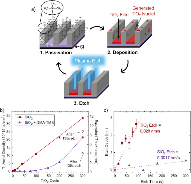
In a groundbreaking study, researchers have made significant advancements in the area-selective deposition (ASD) of TiO2 films, bringing unprecedented uniformity and selectivity to nanoelectronics manufacturing. The research, led by Rachel A. Nye and her team at imec, KU Leuven, and North Carolina University, demonstrates the successful implementation of passivation + deposition + etch supercycle process in industrially relevant 45 nm half-pitch patterns.


By leveraging the unique capabilities of the DMA-TMS inhibitor, the researchers achieved remarkable results. The TiO2 atomic layer deposition (ALD) process yielded a 2× improvement in film thickness, depositing approximately 8 nm of TiO2 with 88% uniformity and 100% selectivity on SiO2/TiN line/space patterns. Moreover, the study revealed lower defectivity on pattern sidewalls, top surfaces, and corners compared to previous reports.

A key finding was pattern-dependent uniformity, emphasizing the significance of understanding and optimizing processes at specific feature scales. As feature sizes continue to shrink, the researchers anticipate further improvements in uniformity. The study also highlighted the importance of refining passivation, deposition, and etch parameters for enhanced selectivity and uniformity control.

The research opens doors to a wide range of applications for TiO2 thin films in nanoelectronics, including antireflection coatings, sensors, photocatalysts, and etch-resistant layers. The study provides valuable insights into the quantification of uniformity and selectivity in nanoscale patterns, serving as a benchmark for future advancements in nanoscale ASD. The results have significant implications for the design and fabrication of electronic devices on an industrial scale.

Tuesday, June 13, 2023

EUV Lithography Embraces Sustainability with Hydrogen Recycling System

Edwards Vacuum and Imec Develop Reverse Fuel Cell to Recycle Contaminated Hydrogen in Chip Manufacturing

The semiconductor industry relies heavily on extreme ultraviolet (EUV) lithography systems to increase transistor density. These systems use large amounts of hydrogen to sweep away contaminants and maintain the cleanliness of their optics. Currently, the contaminated hydrogen is burned to form water, requiring a constant supply of new hydrogen. However, this process contributes to carbon emissions as most hydrogen is produced from natural gas using steam processing.
“It’s similar to a fuel cell, in reverse.”—Anthony Keen, Edwards Vacuum
To address this issue, engineers at Edwards, a vacuum systems firm based in England, have developed a hydrogen recovery system that can recycle up to 80 percent of the gas. The system functions similarly to a fuel cell but in reverse. The contaminated hydrogen is mixed with moisture and nitrogen, ionized, and then forced through a proton-exchange membrane using an electric field. On the other side of the membrane, the protons recombine with electrons to form pure hydrogen, while contaminants and water remain on the other side and can be disposed of properly. The recovered hydrogen can then be sent back to the EUV lithography system.


Edwards collaborated with Imec, a research and innovation hub for nanoelectronics and digital technologies, to test the recovery system. The tests conducted on Imec's silicon pilot line demonstrated that the system recovered 70 to 80 percent of the hydrogen and resulted in a net reduction in energy consumption.

The implementation of this hydrogen recovery system in the semiconductor industry could help lower the environmental footprint of EUV lithography systems and contribute to reducing the carbon emissions associated with chip manufacturing. The semiconductor industry has been striving to reduce its carbon footprint, with estimates suggesting it could account for 3 percent of global emissions by 2040. Edwards will need to make a case to top chipmakers, such as Intel, Samsung, and TSMC, to adopt this green technology and further promote sustainability in chip production.

Sources: 

Global 300mm Fab Equipment Spending to Reach Record $119 Billion in 2026, Fueled by Strong Demand for High-Performance Computing and Automotive Applications

 Korea Leads the Way, Foundry and Memory Sectors Drive Expansion

  • Global 300mm fab equipment spending is projected to reach a record high of $119 billion in 2026, driven by strong demand for high-performance computing, automotive applications, and improved memory requirements.
  • Korea is expected to lead global 300mm fab equipment spending in 2026, followed by Taiwan, China, and the Americas, with the foundry and memory sectors playing significant roles in the expansion.
The global 300mm fab equipment spending is expected to soar to an unprecedented level of $119 billion by 2026, after experiencing a temporary decline in 2023. This remarkable growth is primarily attributed to the surging demand for high-performance computing and automotive applications, coupled with an overall improvement in the demand for memory.


The foundry and memory sectors are poised to be major catalysts in this expansion, signaling a widespread need for semiconductor chips across various end markets and applications. These sectors will drive significant investment in 300mm fab equipment, ensuring the industry's capacity to meet the escalating demand.

In terms of regional spending, Korea is anticipated to lead the global 300mm fab equipment market in 2026. With its well-established semiconductor industry and technological prowess, Korea is well-positioned to capitalize on the increasing demand for chips. Following closely behind Korea, Taiwan, China, and the Americas are expected to contribute substantially to the global spending.

Among the different segments, the foundry sector is projected to witness the highest equipment spending. As the demand for custom-designed chips continues to surge, foundries will invest heavily in advanced manufacturing equipment to meet the diverse needs of their customers. The memory sector is also set to experience robust equipment spending, driven by the growing demand for high-capacity memory solutions in various applications, including data centers, artificial intelligence, and Internet of Things (IoT) devices.

While the foundry and memory sectors thrive, other segments may face modest growth or even decline. This suggests a shifting landscape within the semiconductor industry, with specific sectors driving the overall growth while others adapt to changing market dynamics.

In conclusion, the global 300mm fab equipment spending is poised to reach unprecedented heights in 2026, driven by the strong demand for high-performance computing, automotive applications, and improved memory requirements. Korea is expected to lead the global spending, with the foundry and memory sectors playing pivotal roles in the expansion. This remarkable growth underscores the critical importance of semiconductor chips across a wide range of industries and highlights the need for substantial investment in advanced manufacturing capabilities to meet future demands.

Monday, June 12, 2023

Merck Showcases Expertise in Thin Film Deposition and Atomic Layer Etching at AVS ALD 2023 Conference

Leading scientists and engineers from MERCK present papers on advanced materials and semiconductor processing techniques at AVS ALD/ALE 2023.

Merck, a global science and technology company, is set to participate as a sponsor in the 23rd International Conference on Atomic Layer (ALD/ALE) 2023 organized by the Association for Science and Technology of Materials, Interfaces & Processing (AVS). The conference focuses on the science and technology of atomic layer-controlled deposition of thin films and related topics such as atomic layer etching.

Merck's leading engineers and experts will present their research papers at the conference, covering a wide range of cutting-edge topics. Thong Ngo, a Senior Process Engineer, will discuss the synthesis of 2D MoSe2 by atomic layer deposition on a wafer scale. Randall Higuchi, a Process Engineer, will present an evaluation of Zr and Hf precursors with higher thermal stability for atomic layer deposition of ZrO2 and HfO2 films.

Ravi Kanjolia, a Technology Fellow at Merck, will explore the reverse templating effects of low-resistivity Ru Ald on sputtered Ru, while Haripin Chandra, a Senior R&D Manager, will discuss the properties of VHF PEALD silicon nitride film deposited by precursors with different amino ligands. Martin McBriarty, a Materials Scientist, will present on thermal ALE reactants for semiconductor processing, and Ravi Kanjolia will also discuss crystalline gallium nitride deposition on SiO2/Si by RF-biased atomic layer annealing.


Furthermore, Haripin Chandra will participate in the Emerging Materials Session, focusing on EUV lithography materials. Merck's experts will offer valuable insights and share their expertise with the conference attendees, contributing to the advancement of thin film deposition and atomic layer-controlled processes.


Merck's presence at AVS ALD 2023 demonstrates the company's commitment to advancing technology and providing innovative materials solutions. Attendees will have the opportunity to connect with Merck's experts on-site for personalized advice and support. The conference, being held from July 23 to July 26, 2023, in Bellevue, Washington, promises to facilitate knowledge exchange and foster collaborations among scientists and industry professionals in the field of atomic layer-controlled deposition.

Source: The 23rd International Conference on Atomic Layer (ALD/ALE) 2023 | Merck (merckgroup.com)

Black Ultra-Thin Crystalline Silicon Wafers Achieve Maximum Absorption Limit for Improved Solar Cell Efficiency

State-of-the-art black silicon nanotexture enables ultra-thin silicon photovoltaics with enhanced light trapping and improved performance.

Finnish and Spanish researchers have made a breakthrough in the development of ultra-thin crystalline silicon wafers for solar cells by reaching the maximum theoretical absorption limit using advanced black silicon nanotexture. The achievement not only addresses the challenge of maintaining high absorption in thin wafers but also offers significant cost reductions in the photovoltaic industry. The study demonstrates that wafer thicknesses as low as 10 µm can achieve ideal light trapping.


a) Measured absorption of thin silicon wafers (10, 20, and 40 µm nominal thickness) with polished surfaces (orange) and with black silicon texture etched on the front side (blue). Solid and dashed lines represent absorption with and without back a reflector, respectively. The dotted line corresponds to Yablonovitch's 4n2 absorption limit. b) Scanning electron microscope (SEM) image, bird's eye view, of the black silicon nanotexture obtained by DRIE. The scale bar represents 1 µm. c) A free-standing 10µm-thick black silicon wafer, where its high flexibility can be appreciated. d,e) Top view of two 10 µm wafers: d) textured with black silicon and e) out-of-the-box with polished surfaces.

Reducing wafer thickness is a key strategy for cutting costs in the crystalline silicon photovoltaic industry. Thinner wafers significantly reduce substrate-related expenses. However, the weak absorption of silicon at long wavelengths poses a challenge when reducing wafer thickness. To overcome this, the researchers employed black silicon nanotexture, generated through deep reactive ion etching (DRIE) at cryogenic temperatures. The nanotexture allows for better light management and extends the optical path through internal dispersion and scattering, thus improving photon absorption.

The study also includes the implementation of black silicon nanotexture in an interdigitated back-contacted (IBC) solar cell. The proof-of-concept cell, encapsulated in glass, achieved an impressive 16.4% efficiency, representing a 43% increase in output power compared to a reference polished cell. The results highlight the potential of black silicon nanotexture for future ultra-thin silicon photovoltaics, offering both economic savings and improved cell efficiency.

Conventional techniques like chemical texturization through random pyramids and advanced nanopatterning methods have limitations in terms of material consumption, surface damage, and cost. Black silicon nanotexture produced through cryogenic DRIE offers several advantages, including minimal silicon consumption, low surface recombination, and compatibility with high-efficiency IBC solar cell structures. The researchers successfully applied black silicon nanotexture to ultra-thin monocrystalline substrates, demonstrating its potential for mass-produced ultra-thin crystalline silicon photovoltaics.

This study contributes to the ongoing efforts to make solar energy more cost-effective and efficient. The use of black silicon nanotexture in ultra-thin silicon wafers opens up new possibilities for next-generation solar cell technologies, paving the way for widespread adoption of renewable energy solutions. 

Source: 

Black Ultra-Thin Crystalline Silicon Wafers Reach the 4n2 Absorption Limit–Application to IBC Solar Cells

First published: 31 May 2023
 

Black Ultra‐Thin Crystalline Silicon Wafers Reach the 4n2 Absorption Limit–Application to IBC Solar Cells - Garín - Small - Wiley Online Library

Tokyo Electron Introduces Breakthrough Memory Channel Hole Etch Technology for 3D NAND Flash, Reducing Global Warming Potential by 84%

Tokyo Electron's Innovative Etch Process Enables Ultra-fast 10-µm-deep Etching for 3D NAND Flash with Over 400 Layers, Showcased at Symposium on VLSI Technology and Circuits

Tokyo Electron (TEL) has achieved a significant technological milestone by developing a cutting-edge etch technology capable of creating memory channel holes in advanced 3D NAND devices with over 400 layers. This breakthrough process, pioneered by the development team at Tokyo Electron Miyagi, leverages cryogenic temperatures to achieve exceptionally high etch rates, marking the first time dielectric etch application has been utilized in this temperature range.

The groundbreaking technology not only enables the etching of memory channel holes up to 10 µm deep with a high aspect ratio in just 33 minutes but also boasts an impressive 84% reduction in global warming potential compared to previous methods. The etched structure exhibits well-defined geometry, as demonstrated by cross-section SEM and FIB cut images.


Cross section SEM image of memory channel hole pattern after etching, and FIB cut image at the hole bottom.

TEL's research team behind this groundbreaking technology will present their findings at the prestigious 2023 Symposium on VLSI Technology and Circuits, a renowned international conference on semiconductor research. Their contribution showcases the potential for even larger capacity 3D NAND flash memory.

The presentation, titled "Beyond 10 µm Depth Ultra-High Speed Etch Process with 84% Lower Carbon Footprint for Memory Channel Hole of 3D NAND Flash over 400 Layers," will be delivered by Y. Kihara, M. Tomura, W. Sakamoto, M. Honda, and M. Kojima from Tokyo Electron Miyagi Ltd. The session, scheduled for Tuesday, June 13, from 2 p.m. to 3:40 p.m., will take place in the NAND Flash section of the Technology Session 3 [Shunju II].

For detailed event information about the 2023 Symposium on VLSI Technology and Circuits, please click here. Stay tuned for TEL's technology presentation, which combines semiconductor advancements and environmental protection efforts. 2023 Symposium on VLSI Technology and Circuits

Source: Tokyo Electron Develops Memory Channel Hole Etch Technology That Enables Ultra-fast 10-µm-deep Etching for 3D NAND Flash with Over 400 Layers and an 84% Reduction of Global Warming Potential | News Room | Tokyo Electron Ltd. (tel.com)