Thursday, May 29, 2014

New industrial ALD processes from Picosun

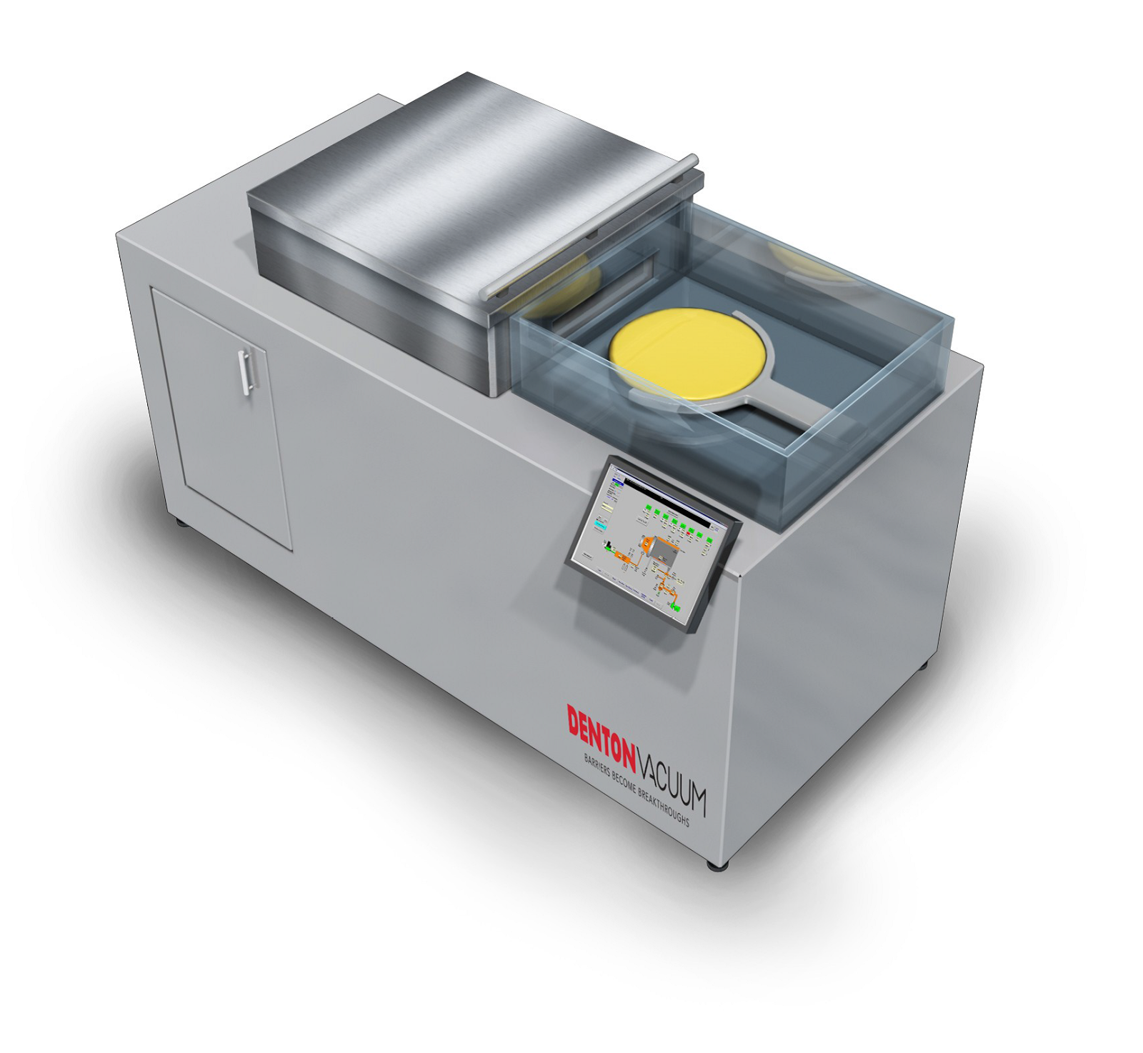
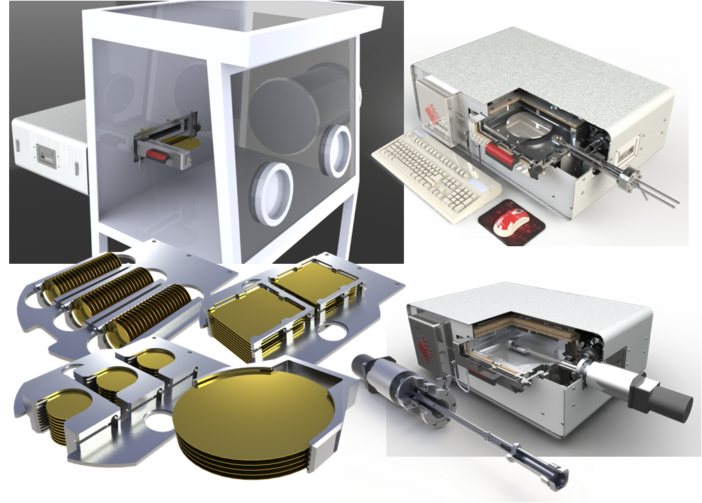
Picosun reports that they now offers new industrial ALD processes for copper and niobium oxide using the 2nd generation of the Picohot™ 300 source system.


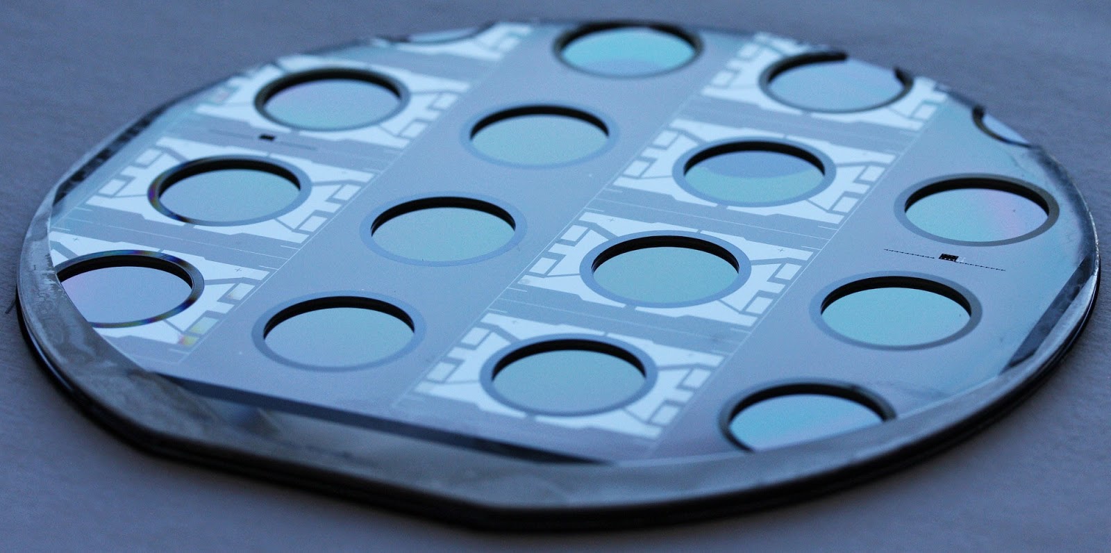
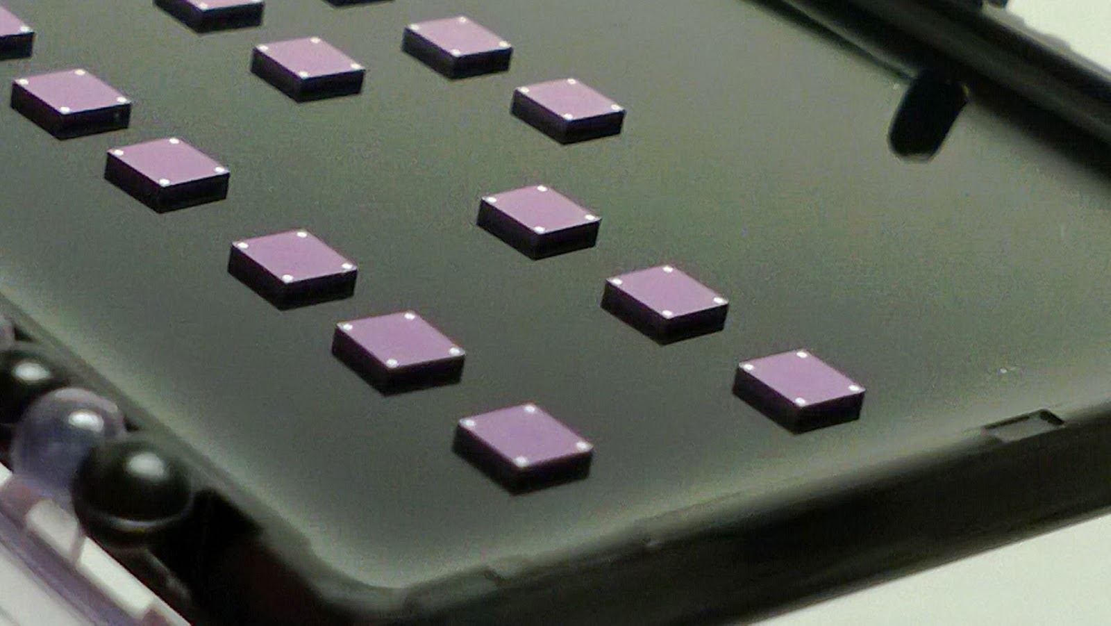
Ultra-thin copper films with the highest level of uniformity and conformality only ALD can offer as a thin film deposition method are a crucial element in today’s and future’s microelectronics and MEMS (microelectromechanical sensors) manufacturing. Copper metallization and seed layers are needed in e.g. microprocessors and 3D-integrated microelectronic components as interconnects. Niobium oxide (Nb2O5), on the other hand, is ideal for moisture and corrosion protection due to its hardness and chemical resistance. 

The now developed low temperature (below 150 °C) thermal ALD processes for niobium oxide and copper have been enabled by Picosun’s newest generation of precursor source design. The 2nd generation of the Picohot™ 300 source system allows even lower vaporization temperatures and efficient, uniform distribution of the precursor vapor in the reaction chamber even at low substrate temperatures.

“Our new processes for copper and niobium oxide show again the excellent quality of Picosun’s precursor source design, allowing true ALD processing also on thermally sensitive materials such as plastics and piezoelectrical elements. On several of Picosun’s main market areas such as MEMS, microelectronics, and corrosion protection, these processes further solidify our status as the leading solution provider of the thin film coating needs of today’s industries,” states Juhana Kostamo, Managing Director of Picosun.

Picosun’s highest level ALD thin film technology enables the industrial leap into the future by novel, cutting-edge coating solutions, with four decades of continuous, groundbreaking expertise in the field. Today, PICOSUN™ ALD systems are in daily production use in numerous prominent industries around the globe. Picosun is based in Finland, with subsidiaries in USA, China, and Singapore, and a world-wide sales and support network.

Wednesday, May 28, 2014

RWTH Aachen fabricate ferroelectric hafnium oxide by chemical solution deposition

RWTH Aachen fabricate ferroelectric hafnium oxide with a remnant polarization of >13 μC/cm2 by chemical solution deposition - to be specific - a yttrium-doped hafnium oxide films on platinum electrodes. This work opens up opportunities for applications using a thicker ferroelectric material than for ALD films at about 10nm that has been developed recent years by NaMLab and Fraunhofer IPMS-CNT.


Chemical solution deposition of ferroelectric yttrium-doped hafnium oxide films on platinum electrodes

S. Starschich, D. Griesche, T. Schneller, R. Waser and U. Böttger

Appl. Phys. Lett. 104, 202903 (2014): http://dx.doi.org/10.1063/1.4879283, Published online 21 Mai 2014

Abstract: Ferroelectric hafnium oxide films were fabricated by chemical solution deposition with a remnant polarization of >13 μC/cm2. The samples were prepared with 5.2 mol. % yttrium-doping and the thickness varied from 18 nm to 70 nm. The hafnium oxide layer was integrated into a metal-insulator-metal capacitor using platinum electrodes. Due to the processing procedure, no thickness dependence of the ferroelectric properties was observed. To confirm the ferroelectric nature of the deposited samples, polarization, capacitance, and piezoelectric displacement measurements were performed. However, no evidence of the orthorhombic phase was found which has been proposed to be the non-centrosymmetric, ferroelectric phase in HfO2.

Monday, May 26, 2014

T. Suntola, "From ideas to global industry" BALTIC ALD, May 12-13, 2014, University of Helsinki

Dr. Tuomo Suntola, has shared his opening presentation "From ideas to global industry" from the recently held Baltic ALD conference, May 12-13, 2014, University of Helsinki [thanks Riikka for sharing].
 
BALTIC ALD, May 12-13, 2014, University of Helsinki
(some snapshots form the presentation that I find especially interesting, follow the link for the complete presentation)
 
 
In late 1973 instrumentarium Oy was searching for new challenges. 1.1.1974 a research unit headed by Tuomo Suntola was formed and The Proposal was given to the board by Dr. Tuomo Sunola: "Let´s develop an electroluminicent flat panel display...nobody has done it yet"


The famous picture of Sven Lindfors, today Chief Technology Officer and a Member of the Board of Directors of Picosun.“We had numerous unsuccessful test runs behind us. Dr. Tuomo Suntola knew that in order to proceed, we needed to advance from using pure chemical elements to an exchange reaction based on carrier gases and sulphides,” says Sven Lindfors, at the time working as a key technician for Dr Suntola’s team. (Source Picosun Newsletter :  http://www.picosun.com/binary/file/-/id/3/fid/79/).


Introduction of high-k materials by ALD in the semiconductor industry for DRAM Capacitors and MOSFETs and the contribution of ALD to the learning curve to keep up with Moore's Law.
 
Follow this link for an overvie on his work concerning Atomic Layer Deposition and thin film devices. The page includes articles, books patents, and conference presentation material from Dr. Tuomo Suntola. ranging back to the early 70s: http://www.sci.fi/~suntola/ald.html

Additional ALD presentations given by Tuomo Suntola in the last 10 years that can also be downloaded from this page:

 T. Suntola, "30 years of ALD"
ALD 2004 Conference, University of Helsinki
 
Russian-Finnish Scientific Conference, 12 – 13 September 2007, Helsinki
 
T. Suntola, "35 years of ALD"
Winter-School Picosun World Forum, 9-10 June 2009, Espoo
 
ENHANCE - Winter-School 9-12 January 2012, University of Helsinki


Sunday, May 25, 2014

Integration of thulium silicate for enhanced scalability of HKMG CMOS technology

A very interesting fresher than fresh PhD Thesis from Royal Institute of Technology (KTH), Sweden on the Integration of thulium silicate for enhanced scalability of high-k/metal gate CMOS technology. The ALD processing in this work has been preformed in a  Beneq TFS 200 ALD system - a crossflow-type 200mm hot-wall reactor. The public defense will take place on 27 May 2014 at 10.00 a.m. in Sal D, Forum, Kungliga Tekniska Högskolan, Isafjordsgatan 39, Kista. - Best of luck!
 

Left, the process flow and right a TEM cross-section of the TmSiO/HfO2/TiN gate stack implemented in gate-last MOSFETs. (From the thesis below)


Integration of thulium silicate for enhanced scalability of high-k/metal gate CMOS technology
EUGENIO DENTONI LITTA
Doctoral Thesis in Information and Communication Technology, Stockholm, Sweden 2014

Abstract: High-k/metal gate stacks have been introduced in CMOS technology during the last decade in order to sustain continued device scaling and ever improving circuit performance. Starting from the 45nm technology node, the stringent requirements in terms of equivalent oxide thickness and gate current density have rendered the replacement of the conventional SiON/poly-Si stack unavoidable. Although Hf-based technology has become the de facto industry standard for high-k/metal gate MOSFETs, problematic long-term scalability has motivated the research of novel materials and solutions to fulfill the target performances expected of gate stacks in future technology nodes. In this work, integration of a high-k interfacial layer has been identified as the most promising approach to improve gate dielectric scalability, since this technology presents the advantage of potential compatibility with both current Hf-based and plausible future higher-k materials. Thulium silicate has been selected as candidate material for integration as interfacial layer, thanks to its unique properties which enabled the development of a straightforward integration process achieving well-controlled and repeatable growth in the sub-nm thickness regime, a contribution of (0.25 ± 0.15)nm to the total EOT, and high quality of the interface with Si. Compatibility with industry-standard CMOS integration flows has been kept as a top priority in the development of the new technology. To this aim, a novel ALD process has been developed and characterized, and a manufacturable process flow for integration of thulium silicate in a generic gate stack has been designed. The thulium silicate interfacial layer technology has been verified to be compatible with standard integration flows, and fabrication of high-k/metal gate MOSFETs with excellent electrical characteristics has been demonstrated. The possibility to achieve high performance devices by integration of thulium silicate in current Hf-based technology has been specifically demonstrated, and the TmSiO/HfO2 dielectric stack has been shown to be compatible with the industrial requirements of operation in the sub-nm EOT range (down to 0.6nm), reliable device operation over a 10 year expected lifetime, and compatibility with common threshold voltage control techniques. The thulium silicate interfacial layer technology has been especially demonstrated to be superior to conventional chemical oxidation in terms of channel mobility at sub-nm EOT, since the TmSiO/HfO2 dielectric stack achieved 20% higher electron and hole mobility compared to state-of-the-art SiOx/HfO2 devices at the same EOT. Such performance enhancement can provide a strong advantage in the EOT-mobility trade-off which is commonly observed in scaled gate stacks, and has been linked by temperature and stress analyses to the higher physical thickness of the high-k interfacial layer, which results in attenuated remote phonon scattering compared to a SiOx interfacial layer achieving the same EOT.


Durable and safe cathode material enabled by ALD for the next-generation electric vehicles

Researchers at University of Colorado at Boulder, Brookhaven National Laboratory, and Seoul National University, has shown that a Al2O3 coating deposited by Atomic Layer Deposition (ALD) dramatically reduces the degradation in cell conductivity and reaction kinetics of commercially available cathode material used in today's state-of-art Li-ion batteries, lithium nickel–manganese–cobalt oxide Li[Ni1/3 Mn1/3Co1/3]O2 a.k.a. NMC.
 
According to the researchers the use of NMC cathodes for plug-in hybrid electric vehicles (PHEVs) and electric vehicles (EVs), have not been possible so far because of: 
  • limited power performance (rate capability)
  • degradation in their capacity and cycle-life at high operation temperatures and voltages
The researches have developed a new durable ultra-thin Al2O3-ALD coating layer that also improves stability for the NMC at an elevated temperature. Furthermore, the experimental results suggest that a highly durable and safe cathode material enabled by atomic-scale surface modification can meet the demanding performance and safety requirements of next-generation electric vehicles.
 

The University of Colorado Boulder (also commonly referred to as CU-Boulder, CU, Boulder, or Colorado) is a public research university located in Boulder, Colorado, United States. It is the flagship university of the University of Colorado system and was founded five months before Colorado was admitted to the union in 1876. According to The Public Ivies: America's Flagship Public Universities (2001), it is considered one of the thirty "Public Ivy League" schools. (Source: Wikipedia, Picture :  The  Campus of University of Colorado Boulder, http://www.colorado.edu/).
 
The work has been funded by by National Science Foundation (USA), Department of Energy (USA), and Ministry of Knowledge Economy (KOR).
 
Results have been published in the article below in the Journal of Power Sources:
 
Ji Woo Kim, Jonathan J. Travis, Enyuan Hu, Kyung-Wan Nam, Seul Cham Kim, Chan Soon Kang, Jae-Ha Woo, Xiao-Qing Yang, Steven M. George, Kyu Hwan Oh, Sung-Jin Cho, Se-Hee Lee
Journal of Power Sources, Volume 254, 15 May 2014, Pages 190–197
 
Abstract: Electric-powered transportation requires an efficient, low-cost, and safe energy storage system with high energy density and power capability. Despite its high specific capacity, the current commercially available cathode material for today's state-of-art Li-ion batteries, lithium nickel–manganese–cobalt oxide Li[Ni1/3 Mn1/3Co1/3]O2 (NMC), suffers from poor cycle life for high temperature operation and marginal rate capability resulting from irreversible degradation of the cathode material upon cycling. Using an atomic-scale surface engineering, the performance of Li[Ni1/3Mn1/3Co1/3]O2 in terms of rate capability and high temperature cycle-life is significantly improved. The Al2O3 coating deposited by atomic layer deposition (ALD) dramatically reduces the degradation in cell conductivity and reaction kinetics. This durable ultra-thin Al2O3-ALD coating layer also improves stability for the NMC at an elevated temperature (55 °C). The experimental results suggest that a highly durable and safe cathode material enabled by atomic-scale surface modification could meet the demanding performance and safety requirements of next-generation electric vehicles.
 
More interesting publications from The Electrochemical Energy Laboratory at University of Colorado at Boulder  on high performance materials for sustainable energy applications :  batteries, supercapacitors, fuel cells, electrochromic winodws, and photoelectrochemical devices can be found here: http://www.colorado.edu/mechanical/ecel/publication.html
  

Saturday, May 24, 2014

Video explaining The Beneq TFS 200 Thin Film System for ALD

As recently published by Beneq: The Beneq TFS 200 Thin Film System for atomic layer deposition (ALD) is the most flexible and upgradable ALD system on the market. Some of its features include:
  • Up to 3 liquid sources
  • 8 gas lines
  • Hot sources
  • Thermal reaction chamber with load lock

Friday, May 23, 2014

ASM International "One cannot think now, the world without Atomic Layer Deposition"

ASM International, one of the leading suppliers of ALD equipment for the semiconductor market has recently updated its web appearance. There are a number of videos that give insights in how ASM and the employees are innovating in the Semiconductor ALD market. And don´t forget - the best page for all Pulsar fans - The switch is on: http://asmtheswitchison.com/.
 

Check out the Vimeo Channel here: http://vimeo.com/user17485889/videos/page:1/sort:date

Here are some of my favourites:

 
Tanja talks about the Thermal Products business unit and how being ‘fast, first and the best’ with ASM innovations like Atomic Layer Deposition (ALD) inspires her.
Tanja, Senior Product Director
 

“I expect innovation from everyone.” Suvi who is recognized, globally, as a pioneering expert in Atomic Layer Deposition (ALD) gives us an insight into her world.
Suvi, Executive Scientist


Doug explains about marketing Atomic Layer Deposition (ALD) technology and the benefits of working at such a diverse, global company like ASM.
Doug, Senior Product Marketing Manager

MIT shows a new promising way to make sheets of graphene on wafers by CVD

MIT News reports - Now researchers at MIT and the University of Michigan have come up with a way of producing graphene, in a process that lends itself to scaling up, by making graphene directly on materials such as large sheets of glass. The process is described, in a paper published this week in the journal Scientific Reports, by a team of nine researchers led by A. John Hart of MIT. Lead authors of the paper are Dan McNerny, a former Michigan postdoc, and Viswanath Balakrishnan, a former MIT postdoc who is now at the Indian Institute of Technology.

The new work, Hart says, still uses a metal film as the template — but instead of making graphene only on top of the metal film, it makes graphene on both the film’s top and bottom. The substrate in this case is silicon dioxide, a form of glass, with a film of nickel on top of it.
 
Using chemical vapor deposition (CVD) to deposit a graphene layer on top of the nickel film, Hart says, yields “not only graphene on top [of the nickel layer], but also on the bottom.” The nickel film can then be peeled away, leaving just the graphene on top of the nonmetallic substrate.
 
This way, there’s no need for a separate process to attach the graphene to the intended substrate — whether it’s a large plate of glass for a display screen, or a thin, flexible material that could be used as the basis for a lightweight, portable solar cell, for example. “You do the CVD on the substrate, and, using our method, the graphene stays behind on the substrate,” Hart says.
 
Read all details about this new approach to manufacture sheets of graphene in the open access Scientific Reports article below.
 
 
a) Process schematic, indicating Ni grain growth during annealing in He, followed by graphene growth under CVD conditions, and then removal of Ni using adhesive tape. Photos of substrates (~1 × 1 cm) and delaminated Ni films in case of b) ex situ tape delamination after graphene growth and c) in situ delamination during the graphene growth step. In the latter case the Ni film retains its integrity upon delamination and is moved to the side using tweezers after the sample is taken from the CVD system. (picture and caption from article below) 
Directfabrication of graphene on SiO2 enabled by thin film stress engineering
Daniel Q. McNerny, B. Viswanath, Davor Copic, Fabrice R. Laye, Christophor Prohoda, Anna C. Brieland-Shoultz, Erik S. Polsen, Nicholas T. Dee, Vijayen S. Veerasamy, A. John Hart   
Scientific Reports, Volume: 4, Article number: 5049, DOI:doi:10.1038/srep05049, Published

Abstract: We demonstrate direct production of graphene on SiO2 by CVD growth of graphene at the interface between a Ni film and the SiO2 substrate, followed by dry mechanical delamination of the Ni using adhesive tape. This result is enabled by understanding of the competition between stress evolution and microstructure development upon annealing of the Ni prior to the graphene growth step. When the Ni film remains adherent after graphene growth, the balance between residual stress and adhesion governs the ability to mechanically remove the Ni after the CVD process. In this study the graphene on SiO2 comprises micron-scale domains, ranging from monolayer to multilayer. The graphene has >90% coverage across centimeter-scale dimensions, limited by the size of our CVD chamber. Further engineering of the Ni film microstructure and stress state could enable manufacturing of highly uniform interfacial graphene followed by clean mechanical delamination over practically indefinite dimensions. Moreover, our findings suggest that preferential adhesion can enable production of 2-D materials directly on application-relevant substrates. This is attractive compared to transfer methods, which can cause mechanical damage and leave residues behind.      

Wednesday, May 21, 2014

Hybrid technology for 2D electronics by graphene/molybdenum disulfide heterostructures grown by CVD

Nanotechweb.org reports that Researchers in the US have unveiled a new CMOS-compatible technology to integrate different two-dimensional materials into a single electronic device. The team, led by Tomás Palacios of the Massachusetts Institute of Technology, constructed large-scale electronic circuits based on graphene and molybdenum sulphide heterostructures grown by chemical vapour deposition where MoS2 was used as a transistor channel, and graphene as contact electrodes and circuit interconnects. The fabrication process itself might be extended to fabricate heterostructures from any type of 2D layered material with potential applications in flexible and transparent electronics, sensors, tunnelling FETs and high-electron mobility transistors.
 
Demonstration of a novel technology for constructing large-scale electronic systems based on graphene/molybdenum disulfide (MoS2) heterostructures grown by chemical vapor deposition.
 
Mor details on this work in the article below:
 
Lili Yu, Yi-Hsien Lee, Xi Ling, Elton J. G. Santos, Yong Cheol Shin , Yuxuan Lin, Madan Dubey, Efthimios Kaxiras, Jing Kong, Han Wang, and Tomás Palacios
Nano Lett., DOI: 10.1021/nl404795z Publication Date (Web): May 8, 2014

Abstract: Two-dimensional (2D) materials have generated great interest in the past few years as a new toolbox for electronics. This family of materials includes, among others, metallic graphene, semiconducting transition metal dichalcogenides (such as MoS2), and insulating boron nitride. These materials and their heterostructures offer excellent mechanical flexibility, optical transparency, and favorable transport properties for realizing electronic, sensing, and optical systems on arbitrary surfaces. In this paper, we demonstrate a novel technology for constructing large-scale electronic systems based on graphene/molybdenum disulfide (MoS2) heterostructures grown by chemical vapor deposition. We have fabricated high-performance devices and circuits based on this heterostructure, where MoS2 is used as the transistor channel and graphene as contact electrodes and circuit interconnects. We provide a systematic comparison of the graphene/MoS2 heterojunction contact to more traditional MoS2-metal junctions, as well as a theoretical investigation, using density functional theory, of the origin of the Schottky barrier height. The tunability of the graphene work function with electrostatic doping significantly improves the ohmic contact to MoS2. These high-performance large-scale devices and circuits based on this 2D heterostructure pave the way for practical flexible transparent electronics.

Monday, May 19, 2014

Vanderbilt University - A Multifunctional Load-Bearing Solid-State Supercapacitor

"The biggest problem with designing load-bearing supercaps is preventing them from delaminating," said Westover. "Combining nanoporous material with the polymer electrolyte bonds the layers together tighter than superglue."
 
Andrew S. Westover, John W. Tian, Shivaprem Bernath, Landon Oakes, Rob Edwards, Farhan N. Shabab, Shahana Chatterjee, Amrutur V. Anilkumar, and Cary L. Pint
Nano Lett., DOI: 10.1021/nl500531r, Publication Date (Web): May 13, 2014


Abstract: A load-bearing, multifunctional material with the simultaneous capability to store energy and withstand static and dynamic mechanical stresses is demonstrated. This is produced using ion-conducting polymers infiltrated into nanoporous silicon that is etched directly into bulk conductive silicon. This device platform maintains energy densities near 10 W h/kg with Coulombic efficiency of 98% under exposure to over 300 kPa tensile stresses and 80 g vibratory accelerations, along with excellent performance in other shear, compression, and impact tests. This demonstrates performance feasibility as a structurally integrated energy storage material broadly applicable across renewable energy systems, transportation systems, and mobile electronics, among others.

Improved supercapacitors using ruthenium oxide RGM foam by University of California

As reported today by Sean Nealon, UC Riverside, Researchers at the Univ. of California, Riverside have developed a novel nanometer scale ruthenium oxide anchored nanocarbon graphene foam architecture that improves the performance of supercapacitors, a development that could mean faster acceleration in electric vehicles and longer battery life in portable electronics.

Read the full story here in the R&D Mag or check out the original OPEN ACCESS publication bellow:
 
Hydrous Ruthenium Oxide Nanoparticles Anchored to Graphene and Carbon Nanotube Hybrid Foam for Supercapacitors
Wei Wang, Shirui Guo, Ilkeun Lee, Kazi Ahmed, Jiebin Zhong, Zachary Favors, Francisco Zaera, Mihrimah Ozkan & Cengiz S. Ozkan          
Scientific Reports 4, Article number: 4452 doi:10.1038/srep04452, 25 March 2014

Abstract: In real life applications, supercapacitors (SCs) often can only be used as part of a hybrid system together with other high energy storage devices due to their relatively lower energy density in comparison to other types of energy storage devices such as batteries and fuel cells. Increasing the energy density of SCs will have a huge impact on the development of future energy storage devices by broadening the area of application for SCs. Here, we report a simple and scalable way of preparing a three-dimensional (3D) sub-5 nm hydrous ruthenium oxide (RuO2) anchored graphene and CNT hybrid foam (RGM) architecture for high-performance supercapacitor electrodes. This RGM architecture demonstrates a novel graphene foam conformally covered with hybrid networks of RuO2 nanoparticles and anchored CNTs. SCs based on RGM show superior gravimetric and per-area capacitive performance (specific capacitance: 502.78 F g−1, areal capacitance: 1.11 F cm−2) which leads to an exceptionally high energy density of 39.28 Wh kg−1 and power density of 128.01 kW kg−1. The electrochemical stability, excellent capacitive performance, and the ease of preparation suggest this RGM system is promising for future energy storage applications.

(a) Schematic illustration of the preparation process of RGM nanostructure foam. SEM images of (b–c) as-grown GM foam (d) Lightly loaded RGM, and (e) heavily loaded RGM. (Source : article above)


Check out the performance in this Ragone plot - Woah - pretty high energy density material!


(a) EIS plots and (b) high frequency region EIS plots of GM, RGM, a control sample (RuO2 nanoparticles only), respectively. (c) Ragone plot related to energy densities and power densities of the packaged whole cell RGM SC, GM SC, RuO2 nanoparticles SC, hydrous ruthenium oxide (RuO2)/graphene sheets composite (GOGSC), RuO2 nanowire/single walled carbon nanotube (SWNT) hybrid film. (Source: articlew above)


Sunday, May 18, 2014

ITRS 2013 Emerging Research Devices on HfO2 based ferroelectric devices

ITRS 2013 Emerging Research Devices (ERD) Chapter has been updated on ferroelectric devices (page 13) referring to recent development using ferroelectric hafnium oxide.

From Page 12 : Notably, since 2011, ferroelectricity in a variety of doped and polycrystalline HfO2 has been reported. The HfO2 based FeFETs show promising write speed (down to a few ns), retention (projected to 10 years), and endurance (up to 1012), which all match the best performances of its perovskite counterparts (refer to ERD4a). [65,66,67,68,69], and HfO2-based FeFETs have been fabricated using standard high-k metal gate (HKMG) processes. The use of HfO2-based ferroelectrics significantly reduces the physical thickness of the gate stack, and in turn scales down the channel length to the current technology node [70]. Follow the typical HKMG process, SiO2 serves as the buffer layer between HfO2 and Si with a sub-nanometer thickness, yielding low depolarization field.

"In Ferroelectric FET memory, a ferroelectric dielectric forms the gate insulator of an FET. The main concern on FeFET memory lies in operation reliability. Operational reliability of the FeFET RAM is limited by the time dependant remnant polarization of the ferroelectric gate dielectric reflected in retention loss. Control of the ferroelectric-semiconductor interface is critical for FeFET properties. The scalability of FeFET memory beyond the 22nm generation is uncertain"

 
As a comparasion to RRAM, one of the main contenders for emerging memory technologies:

 
"RRAM include multiple device types and mechanisms with varying level of maturity. The survey is based on rating of the general field rather than specific types. Some recent breakthrough in RRAM significantly enhanced perceived potential of this technology, e.g., 32Gb array demonstration726. Overall RRAM assessment is similar or better than existing CMOS-based nonvolatile memories (Flash). A clear advantage of RRAM is scalability owing to the filamentary conduction and switching mechanisms. The simple device structure and fab-friendly materials also contribute to high rating in CMOS compatibility. One of the major concerns of RRAM is the operation reliability due to the stochastic nature and the defect-related mechanisms. Large variation of RRAM switching parameters has been commonly observed and is considered an intrinsic feature of RRAM mechanisms."
 
Refernces on FeFET:

[65] T. S. Boscke, J. Muller, D. Brauhaus, U. Schroder, and U. Bottger, "Ferroelectricity in hafnium oxide: CMOS compatible ferroelectric field effect transistors," IEDM 2011, pp. 24.5.1–24.5.4.
[66] M. Hyuk Park, H. Joon Kim, Y. Jin Kim, W. Lee, H. Kyeom Kim, and C. Seong Hwang, "Effect of forming gas annealing on the ferroelectric properties of Hf0.5Zr0.5O2 thin films with and without Pt electrodes," Appl. Phys. Lett., vol. 102, no. 11, p. 112914, 2013.
[67] J. Muller, et al, "Ferroelectricity in yttrium-doped hafnium oxide," J. Appl. Phys., vol. 110, no. 11, p. 114113, 2011.
[68] J. Muller, et al, "Ferroelectric Zr0.5Hf0.5O2 thin films for nonvolatile memory applications," Appl. Phys. Lett., vol. 99, no. 11, p. 112901, 2011.
[69] S. Mueller, J. Mueller, A. Singh, S. Riedel, J. Sundqvist, U. Schroeder, and T. Mikolajick, "Incipient Ferroelectricity in Al-Doped HfO2 Thin Films," Adv. Funct. Mater., vol. 22, no. 11, pp. 2412–2417, Jun. 2012.
[70] J. Muller, E. Yurchuk, T. Schlosser, J. Paul, R. Hoffmann, S. Muller, D. Martin, S. Slesazeck, P. Polakowski, J. Sundqvist, M. Czernohorsky, K. Seidel, P. Kucher, R. Boschke, M. Trentzsch, K. Gebauer, U. Schroder, and T. Mikolajick, "Ferroelectricity in HfO2 enables nonvolatile data storage in 28 nm HKMG," 2012 Symp. VLSI Tech., pp. 25–26, 2012


Emerging memory taxonomy according to ITRS 2013

For all of you working on emerging memory technologies such as ReRAM, FeRAM, PCM, MRAM etc. this classification scheme in the latest ITRS roadmap should be very useful. Please check out the  ERD - Emerging Research Devices Chapter.


"Figure ERD3 [inserted below] provides a simple visual method of categorizing memory technologies. At the highest level, memory technologies are separated by the ability to retain data without power. Nonvolatile memory offers essential use advantages, and the degree to which non-volatility exists is measured in terms of the length of time that data can be expected to be retained. Volatile memories also have a characteristic retention time that can vary from milliseconds to (for practical purposes) the length of time that power remains on. Nonvolatile memory technologies are further categorized by their maturity. Flash memory is considered the baseline nonvolatile memory because it is highly mature, well optimized, and has a significant commercial presence. Flash memory is the benchmark against which prototypical and emerging nonvolatile memory technologies are measured. Prototypical memory technologies are at a point of maturity where they are commercially available (generally for niche applications), and have a large scientific, technological, and systematic knowledge base available in the literature. These prototypical technologies are covered in Table ERD2 and in the PIDS Chapter. The focus of this section is Emerging Memory Technologies. These are the least mature memory technologies in Fig. ERD4, but have been shown to offer significant potential benefits if various scientific and technological hurdles can be overcome. This section provides an overview of these emerging technologies, their potential benefits, and the key research challenges that will allow them to become viable commercial technologies."

 
Figure ERD3, from the ERD Chapter 2013 - Emerging memory taxonomy (ITRS 2013, Chapter ERD
 
If you continue to read from page 8 on you will find a short description of all emerging memory technologies that are being considered by he ITRS. If you´re saturated on resistive technologies you can fast forward to page 12 and read about the new contender FeFET :-)
 

Saturday, May 17, 2014

The new ITRS 2013 edition

The new 2013 edition is now released since about a month Follow this link to the Summary Files. However, not all areas/Chapters has been updated. As an example, for Front End Process (FEP) Chapter the status is as follows:


Updated FEP Roadmap tables are: High Performance Devices, Low Standby Power Devices, FeRAM, Thermal, Thin Film, Doping Process Technology, Starting Materials, and Surface Preparation.
 
"Likely to be updated" in 2014: Updates to DRAM, Floating Gate Flash Non-Volatile memory (NVM), Charge Trap Flash NVM, Phase Change Memory, Etch and CMP.
 
We can assume that Samsung, Hynix, Micron, Toshiba and the guys will have some interesting meetings ahead to conclude what to put in those tables :-)

What is The International Technology Roadmap for Semiconductors - ITRS?

"The International Technology Roadmap for Semiconductors is sponsored by the five leading chip manufacturing regions in the world: Europe, Japan, Korea, Taiwan, and the United States. The sponsoring organizations are the European Semiconductor Industry Association (ESIA), the Japan Electronics and Information Technology Industries Association (JEITA), the Korean Semiconductor Industry Association (KSIA), the Taiwan Semiconductor Industry Association (TSIA), and the United States Semiconductor Industry Association (SIA)."
 
"The objective of the ITRS is to ensure cost-effective advancements in the performance of the integrated circuit and the advanced products and applications that employ such devices, thereby continuing the health and success of this industry."

 
The International Technology Roadmap for Semiconductors is sponsored by the five leading chip manufacturing regions in the world: Europe, Japan, Korea, Taiwan, and the United States. (source : http://www.itrs.net/about.html)

Comments on Twitter:
2013 ITRS executive summary, in the autumn of Moore's Law.
The non-planar future: They 2013 International Technology Roadmap for Semiconductors (ITRS)
ITRS 2013- "The new era of scaling is 3D Power Scaling"
Scouting report for materials at end of the road: 2013 ITRS 


A brief review of atomic layer deposition: from fundamentals to applications

A recent review paper on Atomic Layer Deposition with open access. The review gives an overview of ALD precursors and materials and highlights the following applications: 
  • ALD in microelectronics : high-k gate dielectrics
  • ALD in photovoltaics: buffer layers in Cu(In,Ga)Se2 thin film solar cells
  • ALD in energy storage: Pt and YSZ for solid oxide fuel cells
A brief review of atomic layer deposition: from fundamentals to applications
Richard W. Johnson, Adam Hultqvist, Stacey F. Bent
Materials Today, Available online 10 May 2014

Abstract: Atomic layer deposition (ALD) is a vapor phase technique capable of producing thin films of a variety of materials. Base on sequential, self-limiting reactions, ALD offers exceptional conformality on high-aspect ratio structures, thickness control at the Angstrom level, and tunable film composition. With these advantages, ALD has emerged as a powerful tool for many industrial and research applications. In this review, we provide a brief introduction to ALD and highlight select applications, including Cu(In,Ga)Se2 solar cell devices, high-k transistors, and solid oxide fuel cells. These examples are chosen to illustrate the variety of technologies that are impacted by ALD, the range of materials that ALD can deposit – from metal oxides such as Zn1−xSnxOy, ZrO2, Y2O3, to noble metals such as Pt – and the way in which the unique features of ALD can enable new levels of performance and deeper fundamental understanding to be achieved.
 
 
Different multiple gate design structures where ALD gate oxides have been used. (a) A TEM cross-section of Intel's FinFET transistor at the 22 nm node with the gate-oxide and gate wrapped around the fin. (C. Auth et al. 2012 Symposium on VLSI Technology (VLSIT) (2012), pp. 131–132) (b) Liu et al. omega gate structure wrapping around a Ge channel (B. Liu et al. IEEE Trans. Electron Dev., 60 (6) (2013), pp. 1852–1860) (c) A pi-gate surrounding a poly-Si nanowire in a thin film transistor by Chen et al. (L.-J. Chen et al. IEEE Trans. Nanotechnol., 10 (2) (2011), pp. 260–265) (d) A carbon nanotube FET with a gate all around structure by Franklin et al. (A.D. Franklin et al. Nano Lett., 13 (6) (2013), pp. 2490–2495)
 

Friday, May 16, 2014

Towards all solid-state 3D thin-film batteries for durable and fast storage by imec

An excellent overview on all solid-state 3D thin-film batteries where Philippe Vereecken principal scientist at imec, and associate professor at KU Leuven explains "One way to make Li-ion batteries more durable, safer, smaller and in particularly faster, is a transition towards all solid-state 3D thin-film Li-ion batteries." The article can be find on page 30 in the May 2014 issue of Solid State Technology. UPDATE: this paper is also available here as html Solid State Technology.
 
 
Schematic of a planar (a) and 3D thin-film (b) battery with the following stack: current collector/ electrode/solid electrolyte/electrode/current collector. (Source: Solid State Technology)
 
 
ALD processes for solid state lithium batteries has been and is an active field of research at Oslo and Helsinki University. Below is a recent review from Ola Nilsen et al giving a great overview on the ALD precursor and processes that have been investigated so far.

Ola Nilsen, Ville Miikkulainen, Knut B. Gandrud, Erik Østreng, Amund Ruud, Helmer Fjellvag
Volume 211, Issue 2, pages 357–367, February 2014

The lithium ion battery concept is a promising energy storage system, both for larger automotive systems and smaller mobile devices. The smallest of these, the microbatteries, are commonly based on the all-solid state concept consisting of thin layers of electroactive materials separated by a solid state electrolyte. The fact that solid state electrolytes are required puts rather severe constraints on the materials in terms of electronic and ionic conductivity, as well as lack of pinholes otherwise leading to self-discharge. The atomic layer deposition (ALD) technology is especially suitable for realization of such microbatteries for the Li-ion technology. ALD has an inherent nature to deposit conformal and pinhole free layers on complex geometrical shapes, an architecture most commonly adopted for microbattery designs. The current paper gives an overview of ALD-type deposition processes of functional battery materials, including cathodes, electrolytes, and anodes with the aim of developing all-solid-state batteries. Deposition of Li-containing materials by the ALD technique appears challenging and the status of current efforts is discussed.


ALE - Atomic Layer Etch emerges for 3D NAND, sub-20nm DRAMs and FinFETs

Atomic Layer Etch Finally Emerges - is a interesting blog post by Mark LaPedus (Executive Editor for manufacturing at Semiconductor Engineering) that you should really read if you want some insight into why we need ALE and why it has been difficult to develope this etch technique.
 
After nearly two decades of being confined to R&D labs, equipment makers are placing big bets on this next-gen plasma etch technology.
 
[...]
 
Lam’s Lill agrees that ALE will not replace RIE. “We will offer both technologies in one reactor,” Lill said. “We think they will be complementary for certain applications. But we are already seeing the transition (to ALE) in certain applications.”
 
ALE could be used for 3D NAND, sub-20nm DRAMs and finFETs, but there are still some challenges before ALE is running in the production fab. “There are still three grand challenges left,” Lill said. “One is that there are no secondary unintended reactions for ALE. For example, we don’t want extreme UV radiation in the reactor. Second, we want the unit steps to be discrete. And finally, we need self-limiting single unit steps. They are very difficult to find.”
 
Read more here and additional comments from experts from LAM Research, Applied Materials and Sematech : http://semiengineering.com/atomic-layer-etch-finally-emerges/ 

 
Illustration of the process steps in a plasma-enhanced ALE cycle for a silicon film etched by chlorine and argon. (Source Electroiq)
 
[please note that we used to know ALE as Atomic Layer Epitaxy until ALD - Atomic Layer Deposition took over]

RENA and SoLayTec ship new turnkey InPERC technology order

According to a press release : PV equipment suppliers, RENA and SoLayTec said they had shipped their 10th ‘InPassion’ system to a tier-1 fully integrated PV manufacturer based in China for monocrystalline solar cells.
 
The InPERC turnkey package consists of a complete rear-side smoothing, passivation, capping SiNx and laser ablation solution, which is capable of increasing average conversion efficiencies by more than 0.8%. The technology partners have demonstrated PERC solar cell efficiencies of over 20% with record efficiencies achieved at research centre, ISFH.
 
“It is clear that several PECVD and ALD solutions are available for deposition of Al2O3,” said Roger Görtzen, co-founder of SoLayTec. “SoLayTec  believes that its modular ALD concept has the potential to win the game from PECVD, due to a few important factors. A higher uptime because of less periodic maintenance, 5 times lower usage of TMA precursor material and most important a very high stability of the ALD process. This results into a more narrow efficiency distribution of the cells and a higher average efficiency, leading to a better margin for our customer.”
 
The partners said that they would be presenting the results of their InPERC technology for multicrystalline solar cells with efficiencies above 18% at SNEC 2014. 
 
 
RENA and SoLayTec said they had shipped their 10th ‘InPassion’ system to a tier-1 fully integrated PV manufacturer based in China for monocrystalline solar cells. Image SoLayTec

Thursday, May 15, 2014

Arradiance Introduces GEMstar XT-P™, the First Benchtop PEALD System for Research

As ALD Pulse reports : Arradiance® Introduces Their GEMstar XT-P™, the First Benchtop Thermal and Plasma-Enhanced Atomic Layer Deposition System for Research . The next generation GEMStar XT-P™ provides enhanced thermal and plasma ALD capabilities for cutting-edge nanoscale materials deposition.
 
GEMStar XT-P incorporates a fully functional, remote ICP plasma enhanced ALD capability which enables a broader range of precursor chemistries and ALD films at lower deposition temperatures. The 13.56 MHz plasma source is very compact and air cooled, operating at up to 300 Watts power with an automated matching network. GEMStar XT-P comes standard with three MFC controlled plasma gas lines and one MFC controlled carrier gas line for uniformly depositing even the most challenging oxides, nitrides and metals.
 
 
"Arradiance manufacture Benchtop Atomic Layer Deposition(ALD) Process Systems for a variety of applications. Our systems are designed to deposit uniform, defect free resistive and emissive coatings, even deep inside high aspect ratio (HAR) structures such as Microchannel Plates, Channel Electron Multipliers and Particles. High quality films with ultra-high aspect ratios are key features of our systems." (Source Arradiance.com)

ALD of hematite on Gd2O3 lead to record performance for water splitting electrodes

Omid Zandi and co-workers at the Materials for Energy Conversion Group, Michigan State University are using ALD for the deposition of metal oxide semiconductors, doping and coatings, for solar fuel production purposes. Recent published work in Journal of Physical Letters about solar water oxidation with hematite deposited and modified via ALD allowed them to study and overcome the limitations of this system which led to the record performance reported for hematite based photoanodes recently (J. Phys. Chem. Lett., 2014, 5 (9), pp 1522–1526 below).

Substrate Dependent Water Splitting with Ultrathin α-Fe2O3 Electrodes
Omid Zandi, Joseph A. Beardslee, and Thomas Hamann
J. Phys. Chem. C, Article ASAP

 
Thin films of hematite (α-Fe2O3) were deposited by atomic layer deposition (ALD), and the effects of metal oxide underlayers on the photocatalytic water oxidation performance were investigated. It was found that a Ga2O3 underlayer dramatically enhances the water oxidation performance of the thinnest hematite films. The performance enhancement is attributed to the increased crystallinity of the ultrathin films induced by the oxide underlayers. The degree of crystallinity was examined by Raman line shape analysis of the characteristic hematite phonon modes. It was found that multiple metal oxide underlayers, including Nb2O5, ITO, and WO3, increase the film crystallinity compared to hematite deposited on bare FTO. The increased crystallite size was also clearly evident from the high resolution SEM images. The degree of crystallinity was found to correlate with absorbance and the photocatalytic water oxidation performance. These findings shed light on the origin of the dead layer at the interface of the FTO substrate and ultrathin hematite films and elucidate strategies at overcoming it. (Picture from graphical abstract)

Enhanced Water Splitting Efficiency Through Selective Surface State Removal
Omid Zandi and Thomas W. Hamann
J. Phys. Chem. Lett., 2014, 5 (9), pp 1522–1526
 
 
Hematite (α-Fe2O3) thin film electrodes prepared by atomic layer deposition (ALD) were employed to photocatalytically oxidize water under 1 sun illumination. It was shown that annealing at 800 °C substantially improves the water oxidation efficiency of the ultrathin film hematite electrodes. The effect of high temperature treatment is shown to remove one of two surface states identified, which reduces recombination and Fermi level pinning. Further modification with Co–Pi water oxidation catalyst resulted in unprecedented photocurrent onset potential of 
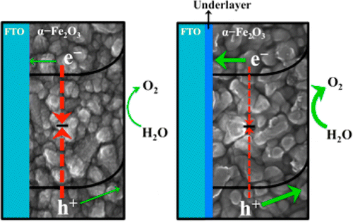
0.6 V versus reversible hydrogen electrode (RHE; slightly positive of the flat band potential). (Picture from graphical abstract).

Growth mechanism and the effect of doping hematite with Ti can be found in this publication: Highly photoactive Ti-doped α-Fe2O3 thin film electrodes: resurrection of the dead layer.


VTT in Finland to spin-off MEMS devices based on novel FABRY-Perot interferometers

According to press release : VTT Technical Research Centre of Finland has developed smart optical measuring devices with companies for uses that include optimisation of vehicle engines, reduction and monitoring of environmental emissions, and quality control of pharmaceuticals. The FABRY research project aimed at utilisation of VTT-developed technologies to enable commercialisation of new products on global markets. So far, two of the companies involved – Rikola Ltd from Finland and InnoPharma Labs from Ireland – have launched products of their own. VTT’s technology makes it possible to miniaturise an entire measuring laboratory to the size of a small sensor.
 
 
Special industry-grade mirror structures realized in the project. (source VTT)
 
Originally, VTT developed these optical measurement technologies and the associated micromechanical Fabry-Perot interferometer components for the purpose of carbon dioxide measurements. The technology has many other applications, however. VTT joined together with eight companies in the Tekes-financed FABRY project in order to create business from the technology in the form of new products.
 
In the course of the project, five of the companies started a product development project of their own based on the project results. So far, two of the companies have launched a new product on the market. Rikola Ltd manufactures and sells the world’s smallest hyperspectral camera, which can be used, for example, for surveying fertilisation and irrigation needs in agricultural areas from UAVs. The Irish InnoPharma Labs manufactures Eyemap cameras for the pharmaceutical industry, facilitating rapid verification of the drug ingredients and their distribution in a tablet.
 
VTT is also in the process of establishing a spin-off company based on this technology, with expected launch in May 2014.
 
“Apart from new business operations, optical measurement technology also has an impact on employment. In the long run, this could create dozens, or maybe even hundreds of new jobs in Finland,” says Jarkko Antila, Senior Scientist at VTT, who has been coordinating the project.
 
 
Tunable MEMS-based Infrared filters. (source VTT)
 
Participants in the 2011–2014 FABRY project (Spectroscopic sensor devices based on novel FABRY-Perot interferometers) coordinated by VTT were Continental Automotive SAS from France (fuel measurements for the automotive industry, onboard sensor); SICK AG from Germany (demanding industrial gas measurements); InnoPharma Labs from Ireland (automatic quality management and control for drug manufacturing in the pharmaceutical industry); Ocean Optics from the United States (optical spectroscopy and Raman spectroscopy); Murata Electronics from Finland (sensor manufacturing for the automotive industry); Rikola Ltd Oy from Finland (cameras for hyperspectral imaging ; manufacturing of spectrometer modules); Okmetic Oyj from Finland (development and manufacturing of high-quality silicon wafer for optical sensor applications) and VTT Memsfab Ltd (manufacturing of MEMS components).
 
Fabry-Perot interferometer
The principle of optical measurement, developed at the end of the 19th century, is a widely used technique, for example in astronomy. Expensive scientific instruments are used to identify and measure different materials based on their characteristic spectral lines, thus obtaining information about the composition of the target. VTT has combined this technology with microelectromechanical systems (MEMS), creating an affordable, very small and adjustable spectral filter. This makes it possible to miniaturise an entire measuring laboratory to the size of a small sensor.
 
Here is a interesting presentation with much more details form Jarkko Antila showing details on ALD MEMS Fabry-Perot interferometer principles and its use for imaging purposes
http://www.vtt.fi/files/newsletter/os/022012/spectral_imaging_device.pdf. It is unclear if this ALD technology is used in the commercial product.

 
Screendump from presentration above

Wednesday, May 14, 2014

How to build your ALD reactors for less than $10,000


A publication on how grad students at Central Michigan University construct ALD reactors for less than $10,000. One hot wall tube reactor and a cold-wall reactor equiped with QCM sensor for in-situ growth studies.

Cost-Effective Systems for Atomic Layer Deposition
Michael Lubitz, Phillip A. Medina, Aleks Antic, Joseph T. Rosin, and Bradley D. 
Publication Date (Web): May 12, 2014
Journal of Chemical Education - (ACS Publications and Division of Chemical Education) http://pubs.acs.org/doi/full/10.1021/ed4007698

Abstract: Herein, we describe the design and testing of two different home-built atomic layer deposition (ALD) systems for the growth of thin films with sub-monolayer control over film thickness. The first reactor is a horizontally aligned hot-walled reactor with a vacuum purging system. The second reactor is a vertically aligned cold-walled reactor with a quartz crystal microbalance (QCM) and a vacuum purging system. This latter reactor was also built to be capable of the addition of liquid- or solution-phase precursors, including the addition of a solution-based precursor containing nanoparticles. Each system cost less than $10,000, and they were used to deposit aluminum oxide thin films using trimethylaluminum and water/isopropyl alcohol as coreactants. Whereas the horizontal hot-walled system was able to deposit alumina thin films at a growth rate of 1.2–1.4 Å/cycle, the more sophisticated vertically aligned reactor deposited films at 0.95–1.1 Å/cycle, which is comparable to commercial systems costing $100,000 or more. Most importantly, both systems were fabricated entirely by M.S. and undergraduate students at Central Michigan University.
 
 
Upper left, a hot-wall tube reactor and right a cold-wall reactor equiped with QCM sensor for in-situ growth studies.(images fromgraphical abstract)  

Monday, May 5, 2014

Denton Vacuum introduces Exilis 1 ALD system

As reported today: Denton Vacuum LLC, a leading manufacturer of thin film technology products, has announced the introduction of Exilis 1, a new atomic layer deposition (ALD) system that will deliver breakthrough results for users in the research, aerospace, optics, semiconductor, and medical communities.
 
DV Model CF-102 ALD Process Chamber (cross-flow thermal). Configured for stand-alone operation or as a Denton Vacuum cluster tool module. Plasma source upgrade will become available in the future (Source Data Sheet).
 
"We've talked to ALD system users all over the world, and they are not happy with what's now available on the market," said Vince McGinty, president and CEO of Denton Vacuum. "Many commercially available ALD systems are limited in capability, while others have proven to be maintenance nightmares, with such simple tasks as chamber cleaning, precursor loading and valve changes turning into complex events that lead to extended, even indeterminate downtime.
"Adding to this," McGinty continued, "users in the corporate community often find that systems designed for research and development bear no resemblance to systems designed for manufacturing-scale activities. Exilis 1 addresses these issues, with broader capability, improved productivity and maintainability, and direct paths to production scale-up."
Denton Vacuum's Exilis 1 brings new capability in several key areas, including:
  • Multi-wafer and 3D component capability.
  • Expanded process chamber adaptability (remote plasma source, a vacuum load lock, and even integration into a Denton cluster tool).
  • An automated load/unload arm that enables immediate, safe removal of hot substrates from the process chamber.
  • Reliable and quick replacement of precursor canisters and ALD valves (the hard-mounted, easy-access manifold incorporates an internal heater assembly, enabling canister or ALD valve changes in less than ten minutes).
For more information regarding Denton's new ALD offering, click here or dwnload the data sheet here.

Sunday, May 4, 2014

Flexible monolayer circuit design by Vanderbilt and ORNL

Vanderbilt University reported - How to create nanowires only three atoms wide with an electron beam - "Junhao Lin, a Vanderbilt University Ph.D. student and visiting scientist at Oak Ridge National Laboratory (ORNL), has found a way to use a finely focused beam of electrons to create some of the smallest wires ever made. The flexible metallic wires are only three atoms wide: One thousandth the width of the microscopic wires used to connect the transistors in today’s integrated circuits."
 
“This will likely stimulate a huge research interest in monolayer circuit design,” Lin said. Because this technique uses electron irradiation, it can in principle be applicable to any kind of electron-based instrument, such as electron-beam lithography.”
 
One of the intriguing properties of monolayer circuitry is its toughness and flexibility. It is too early to predict what kinds of applications it will produce, but “If you let your imagination go, you can envision tablets and television displays that are as thin as a sheet of paper that you can roll up and stuff in your pocket or purse,” Pantelides commented.
 
In addition, Lin envisions that the new technique could make it possible to create three-dimensional circuits by stacking monolayers “like Lego blocks” and using electron beams to fabricate the wires that connect the stacked layers.
 
Full report from Vanderbilt University can be found here and please check out the video and the publication below for more insights!


Series of still scanning electron micrographs (a to d) show how the electron beam is used to create nanowires. (Junhao Lin / Vanderbilt)


Junhao Lin, a Vanderbilt University Ph.D. student and visiting scientist at Oak Ridge National Laboratory (ORNL), has found a way to use a finely focused beam of electrons to create flexible metallic wires that are only three atoms wide: One thousandth the width of the microscopic wires used to connect the transistors in today's integrated circuits and some of the smallest wires ever made. The discovery gives a boost to efforts aimed at creating electrical circuits on monolayered materials, raising the possibility of flexible, paper-thin tablets and television displays. [youtube.com]

Atomic mechanism of the semiconducting-to-metallic phase transition in single-layered MoS2
Yung-Chang Lin, Dumitru O. Dumcenco, Ying-Sheng Huang & Kazu Suenaga        
Nature Nanotechnology (2014) doi:10.1038/nnano.2014.64 Published online 20 April 2014
 
Abstract:
Phase transitions can be used to alter the properties of a material without adding any additional atoms and are therefore of significant technological value. In a solid, phase transitions involve collective atomic displacements, but such atomic processes have so far only been investigated using macroscopic approaches. Here, we show that in situ scanning transmission electron microscopy can be used to follow the structural transformation between semiconducting (2H) and metallic (1T) phases in single-layered MoS2, with atomic resolution. The 2H/1T phase transition involves gliding atomic planes of sulphur and/or molybdenum and requires an intermediate phase (α-phase) as a precursor. The migration of two kinds of boundaries (β- and γ-boundaries) is also found to be responsible for the growth of the second phase. Furthermore, we show that areas of the 1T phase can be controllably grown in a layer of the 2H phase using an electron beam.
 

Saturday, May 3, 2014

3rd China ALD conference Shanghai, October 16 to 17, 2014

The 2nd International Conference on ALD Applications / 3rd China ALD conference will be a two-day meeting, dedicated to the fundamental, materials, and applications of Atomic Layer Deposition (ALD) technology. It will be held in Shanghai, China, from October 16 to 17, 2014. Following the success of the 1st and 2nd China ALD Scientific Meeting in 2010 and 2012, the 3rd China ALD 2014 conference will feature plenary sessions, poster sessions and an industrial exhibition.


Organization Commmittee:

ORGANIZING CHAIRS : Prof. Shi-Jin Ding and Prof. Yongfeng Mei
     
SECRETARY-GENERAL : Asso. Prof. Hongliang Lu and Asso. Prof. Feng Zhang


Invited Speakers (Confirmed)


Prof. Steve George, University of Colorado at Boulder
Title: Spatial Atomic Layer Deposition on Flexible Substrates Using a Modular Rotating Cylinder

Prof. Gregory Parsons, North Carolina University
Title: New Applications and Ab-Initio Reaction Mechanism Analysis for ALD onto Polymer Fibers and Films Abstract

Prof. Erwin Kessels, Technische Universiteit Eindhoven
Title: Surface chemistry during metal ALD: Opportunities for film growth, nanopatterning and nanoparticle synthesis

Prof. Christophe Detavernier, Ghent University
Title: Thermal and Plasma Enhanced Atomic Layer Deposition on Powders Abstract

Prof. Hyeongtag Jeon, Hanyang University
Title: Multi-density ALD Al2O3 Layer for OLED Abstract

Prof. Yukihiro SHIMOGAKI, University of Tokyo

Prof. Peide Ye, Purdue University
Title: ALD for State-Of-The-Art Nanoelectronics Abstract

Prof. Stacey F. Bent, Stanford University
Title: ALD of Nanoscale Materials for Energy Conversion Applications Abstract

Prof. Mato Knez, Nanoscience Cooperative Research Center

Prof. Jane P. Chang, University of California at Los Angeles
Title: Enabling the Synthesis and Integration of Multiferroic Materials by Atomic Layer Processing

Prof. Hyungjun Kim, Yonsei University
Title: Synthesis of 2D Transition Metal Disulfides (TMDSs) Nanosheets using Atomic Layer Deposition Abstract

Prof. Yong Wang, Nanjing Tech University
Title: Atomic layer deposition for the modification and functionalization of separating membranes: chances and challenges Abstract

Prof. Markku Leskela, University of Helsinki
Title: ALD for Energy Applications Abstract

Program is now available here.