Sunday, July 13, 2014

IBM Zürich solves 40+ Year Old Challenge for Phase Change Materials

IBM Research reports in their News Blog on a breakthrough made in understanding and development of phase change memory cells by IBM Research in Zürich. "... for more than 40 years scientists have never measured the temperature dependence of crystal growth, due to the difficulties associated with the measurements which are taken at both a nanometer length and a nanosecond time scale. That was until earlier this year when, for the first time, IBM scientists in Zurich were able to take the measurements, which is today being reported in the peer-review journal Nature Communications."
 
 
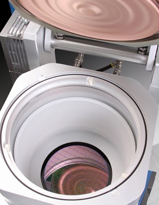
The Binnig and Rohrer Nanotechnology Center is a unique facility for exploratory research. It is not a production or a pilot line with fixed processes or wafer sizes. Rather, it is a state-of-the-art exploratory cleanroom fabrication facility combined with "noise-free" labs shielded against external vibrations, acoustic noise, electromagnetic fields and temperature fluctuations.
 
Please see the abstract to the publication below and check out the blog more details including also an interview with the resreachers at The Binnig and Rohrer Nanotechnology Center in Zürich.
 
  
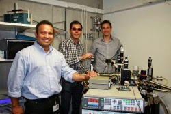
Abu Sebastian, Manuel Le Gallo und Daniel Krebs (Bild: IBM Research)

Abu Sebastian, Manuel Le Gallo, & Daniel Krebs,
Nature Communications Volume: 5, Article number: 4314 DOI:doi:10.1038/ncomms5314, 07 July 2014

In spite of the prominent role played by phase change materials in information technology, a detailed understanding of the central property of such materials, namely the phase change mechanism, is still lacking mostly because of difficulties associated with experimental measurements. Here, we measure the crystal growth velocity of a phase change material at both the nanometre length and the nanosecond timescale using phase-change memory cells. The material is studied in the technologically relevant melt-quenched phase and directly in the environment in which the phase change material is going to be used in the application. We present a consistent description of the temperature dependence of the crystal growth velocity in the glass and the super-cooled liquid up to the melting temperature.
 
 
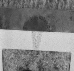
The cross-sectional tunneling  electron microscopy (TEM) image of  a mushroom-type PCM cell  is shown in this photo.
 

Saturday, July 12, 2014

Self assembly of 15,000 semiconductor chips per hour

The Next Big Future Blog reports on a A first automated reel-to-reel fluidic self-assembly process for macroelectronic applications. The system enables high speed assembly of semiconductor dies (15,000 chips per hour using a 2.5 cm wide web) over large area substrates. The optimization of the system (hour 99% assembly yield) is based on identification, calculation, and optimization of the relevant forces. As an application the production of a solid state lighting panel is discussed involving a novel approach to apply a conductive layer through lamination.

A First Implementation of an Automated Reel-to-Reel Fluidic Self-Assembly Machine 
Se-Chul Park , Jun Fang , Shantonu Biswas , Mahsa Mozafari , Thomas Stauden , and Heiko O. Jacobs
Adv. Mater. 2014, DOI: 10.1002/adma.201401573 (Free down load)

In this communication, we report on recent progress towards a fi rst implementation of a self-assembly machine that is based on surface-tension-directed-self-assembly. The reported assembly process is no longer a discontinuous smallbatch hand-operated process but resembles an automated machine like process involving a conveyer belt and a reel-to-reel (RTR) type assembly approach with automated agitation. As a comparison, the assembly rate of conventional chip level pick-and-place machines depends on the cost of the system and number of assembly heads that are used. For example, a highend FCM 10000 (Muehlbauer AG) fl ip chip assembly system can assemble approximately 8000 chips per hour achieving a placement accuracy of 30 μm. 

Our current design achieves 15 k chips per hour using a 2.5 cm wide assembly region which is only a factor of 2 better than one of the faster pick-and-place machines; scaling to 150 k chips per hour, however, would be possible using a 25 cm wide web, which would be a factor of 20 faster. 


In principle, scaling to any throughput should be possible considering the parallel nature of self-assembly. In terms of placement accuracy our precision increase with a reduction of chip and solder bump size. Generally, it exceeds the 30 μm limits for the components that have been used. Under optimized operational conditions, we achieved an assembly yield of 99.8% using the self-assembly process. As an application the assembly machine is applied to the realization of area lighting panels incorporating distributed inorganic light emitting diodes (LEDs).


Friday, July 11, 2014

IBM is investing $3 billion to push the limits of chip technology to 7 nm and beyond

Nanowerk News reports: IBM today announced it is investing $3 billion over the next 5 years in two broad research and early stage development programs to push the limits of chip technology needed to meet the emerging demands of cloud computing and Big Data systems. These investments will push IBM's semiconductor innovations from today's breakthroughs into the advanced technology leadership required for the future.


IBM infoographic

Peeling back the layers of thin film structure and chemistry

Nanowerk News reports: Perovskites — any material with the same structure as calcium titanium oxide (CaTiO3) —continue to entice materials scientists with their ferroelectricity, ferromagnetism, catalytic activity, and oxygen-ion conductivity. In recent years, scientists realized that they could vastly improve the properties of perovskites by assembling them into thin films. The problem was that no one understood why thin films beat out bulk materials.Researchers gained new insight into thin-film superiority by probing the structure of perovskites at the X-ray Science Division 33-ID-D,E x-ray beamline at the U.S. Department of Energy's Advanced Photon Source (APS), Argonne National Laboratory. They used a groundbreaking approach to tease apart the thin-film structure and chemistry layer-by-layer

Read more: Peeling back the layers of thin film structure and chemistry http://www.nanowerk.com/nanotechnology-news/newsid=36506.php#ixzz37BBtO4pz 


                                              Graphical abstract: Revealing the atomic structure and strontium distribution in nanometer-thick La0.8Sr0.2CoO3−δ grown on (001)-oriented SrTiO3


Zhenxing Feng, Yizhak Yacoby, Wesley T. Hong, Hua Zhou, Michael D. Biegalski, Hans M. Christen and Yang Shao-Horn

Surface segregation in metal oxides can greatly influence the oxygen transport and surface oxygen exchange kinetics critical to the performance of solid-state devices such as oxygen permeation membranes and solid oxide fuel/electrolytic cell electrodes. Unfortunately detecting elemental distributions at the atomic scale near the surface remains challenging, which hampers the understanding of underpinning mechanisms and control of surface segregation for the design of high-performance materials. Using the coherent Bragg rod analysis (COBRA) method, we report the first direct 3D atomic imaging of a 4 nm-thick “La0.8Sr0.2CoO3–δ”/SrTiO3epitaxial film. Of significance, energy differential COBRA revealed pronounced Sr segregation (La1−xSrxCoO3−δ, x 0.4) in the four unit cells from the top surface while complete Sr depletion was detected in the five unit cells from the “La0.8Sr0.2CoO3−δ”/SrTiO3 interface. The drastic strontium compositional changes in the film were associated with large changes in the atomic positions of apical oxygen sites in the perovskite structure. Such Sr segregation tendencies toward the surface were also found in nominal “La0.6Sr0.4CoO3−δ” thin films, which can greatly enhance the surface oxygen exchange properties of oxides. The results presented here show that COBRA and the differential COBRA methods can be used to investigate a variety of electrochemically active systems providing atomic scale structural and chemical information that can help understand the physical and chemical properties of these systems and serve as a basis for comparison with DFT calculations.


Tuesday, July 8, 2014

VIDEO from Lam Research - Engineering at the Atomic Scale ALD & ALE

Cool video from the Lam Reaearch blog - Building Chips a Few Atoms at a Time


Snap shot from the animated video below (youtube.com)

"Atomic layer deposition (ALD) and atomic layer etch (ALE) use cycles of multi-step processes to deposit or remove a few atomic layers at a time, providing chipmakers with the process control needed for next-generation device manufacturing. To see how these technologies work, check out our latest video"

HAM-LET is releasing its new Ultra Fast (UF) Diaphragm Valve for ALD

HAM-LET is releasing its new Ultra Fast (UF) Diaphragm Valve for Atomic Layer Deposition and fast switching applications, at Semicon West in San Francisco, booth no. 1539, from 8-10 July.

"Our UF's unique flow adjustment mechanism, patent pending no. US 61/910,79, allows for exceptional flow tuning during operation," said Eran Pintel, VP Marketing and Sales at HAM-LET.


"Another advantage of our UF diaphragm valve is its outstanding durability and low maintenance, as it offers over 100 million life cycles. The UF series meets the demand for high-precision diaphragm valves that can perform accurately and repeatedly over an extremely large number of cycles, required by ALD applications," said Pintel.

The optional extended bonnet and cooling fin provide a superb solution when precise and repeatable performance in high-temperature applications is required. The UF series offers superior sealing performance and remarkable durability in hazardous environments, under severe demands of ultra fast actuation at high purity applications.

HAM-LET will showcase a live demonstration of the UF series at Semicon West 2014, booth no. 1539.

About HAM-LET Group

Founded in 1950, HAM-LET Group specializes in the design, development production and marketing of high quality instrumentation valves and fittings in a wide variety of materials for high pressure, high temperature and vacuum applications. An accent on quality combined with ongoing research and development has given the company an international reputation for excellence. As a result, HAM-LET Group today is the fastest growing company in this industry. We are Totally Committed to our customers providing highest quality products and best of breed service. Our products are used around the world in a wide range of industries, including Energy, Oil & Gas, Ground Turbines, Chemical and Petrochemical, CNG/NGV, Semiconductor, Analytical and others.

Visit us at: http://www.ham-let.com

Imec Achieve Record for n-PERT Solar Cell with Spatial ALD from SoLayTec

As reported today : Nano-electronics research center Imec, reported today an n-type PERT crystalline silicon (Si) solar cell fabricated on a large area wafer (15.6cm x 15.6 cm) reaching a top conversion efficiency of 21.5%(calibrated at ISE CalLab), claiming that this is the highest efficiency achieved for this type of solar cell on an industrial large area wafer size.

This result will accelerate the adoption of n-type PERT (Passivated Emitter, Rear Totally diffused) solar cells in the industry as it clearly shows the potential for improved conversion efficiencies for next generation standard two side contacted crystalline silicon solar cells. Additionally imec researchers showed recently that n-type PERT solar cells of imec, having a rear emitter, are not affected by reliability risks originating from a front Ni/Cu plated metallization.

The cell reaching this 21.5% conversion efficiency had an open circuit voltage (Voc) of 677mV, a short circuit current (Jsc) of 39.1 mA/cm2, and 81.3% fill factor, and features a rear blanket p+ emitter obtained by boron diffusion. Reliable front metal contacts on an n+ front-surface-field are formed by means of Ni/Cu/Ag plating (3 bus bars grid) using an industrial plating tool from Meco, while the rear local contacts to the p+ emitter were obtained by laser ablation of the rear passivation stack and subsequent physical-vapor-deposition of aluminum. The rear passivation stack includes a thin (<10 nm) Atomic-Layer-Deposited (ALD) Al2O3 layer, deposited with the spatial ALD technique InPassion Lab from SoLayTec.

The adoption of ALD Al2O3 based-passivation for the p+ emitter resulted in an average improvement in cell efficiency of about 0.3% absolute with respect to passivation by wet oxidation. This illustrates the excellent capabilities of ALD for passivation layers in next generation cell concepts like PERC and n-type PERT.

These results have been achieved in the framework of the imec’s industrial affiliation program on advanced silicon solar cells, dedicated to developing high performance and low cost Si PV-technologies. In this program, imec works closely together with industrial and academic partners along the solar cell value chain. Via participation and contribution to this program, these partners support Imec’s developments and obtain early access to new technology solutions in this way accelerating their own product development.


Lam's New Products Deliver Critical Capability for Building 3D NAND Memory Devices

As reported today by Lam Research Corp. : Lam Research Corp. today unveiled its latest thin film deposition and plasma etch products for 3D NAND fabrication. As memory customers begin ramping production of these new devices, greater process control is needed for cost-effective manufacturing. Lam's new systems address this need for three of the most critical steps in forming 3D NAND memory cells: stack deposition (VECTOR® Q Strata(tm)), vertical channel etching (2300® Flex(tm) F Series), and tungsten wordline deposition (ALTUS® Max ICEFill(tm)).


The 3D NAND memory structures now moving to production involve numerous pairs of stacked films. Process variability on both the horizontal and vertical planes must be minimized for critical steps so that each memory cell in the final device delivers similar performance. Otherwise, variation in one step can be transferred and multiplied in subsequent steps, compounding errors and leading to poor device performance and low product yield. With 40 or more pairs of films in the stack, carefully managing even slight process fluctuations is essential. Lam's new products address these stringent control requirements.

As memory customers begin ramping production of these new devices, greater process control is needed for cost-effective manufacturing. Lam's new systems address this need for three of the most critical steps in forming 3D NAND memory cells: stack deposition (VECTOR® Q Strata™), vertical channel etching (2300® Flex™ F Series), and tungsten wordline deposition (ALTUS® Max ICEFill™).


The new VECTOR Q Strata PECVD (plasma enhanced chemical vapor deposition) system is used for depositing multilayer film stacks. For this critical 3D NAND process step, the system can perform both oxide/nitride (ONON) and oxide/polysilicon (OPOP) film stack deposition. To deposit the ultra-smooth, uniform films required to avoid compounding errors, the system's matched chambers deliver superior defectivity, film stress, and wafer bow performance. In addition, the VECTOR Q Strata also provides industry-leading productivity with the highest throughput per square meter of fab area available today. As the number of layers in these stacks continues to grow, high productivity is increasingly important for cost-effective production.

Once the stack of paired films is deposited, Lam's 2300 Flex F Series dielectric etch product is used to create a vertical channel through the stack. The new system can etch through high aspect ratio structures with minimal distortion or sidewall damage, while also tightly controlling etch profile uniformity across the wafer. This capability is critical since even small deviations can cause channel dimensions to differ from cell to cell, resulting in device performance variation. A proprietary high ion energy source with modulation of energies enables these results.

The latest in Lam's market-leading tungsten deposition product line, the ALTUS Max ICEFill system controls variability by providing void-free fill of the geometrically complex 3D NAND wordlines. Using a proprietary filling technique, the new system creates the tungsten wordlines with an inside-out atomic layer deposition (ALD) process. The ICEFill process completely fills the lateral (horizontal) lines without any voids, while at the same time minimizing deposition in the vertical channel area. As a result, both electrical performance and yield are enhanced.

"By focusing on collaboration at Lam Research, we are innovating faster and more effectively to deliver the enabling capabilities our customers need," said Rick Gottscho, executive vice president of Global Products. "With the support and expertise of our customers and research partners, Lam now offers three products -- VECTOR Q Strata, 2300 Flex F Series, and ALTUS Max ICEFill -- that are playing critical roles in the development and production ramp of 3D NAND memory devices."

Sunday, July 6, 2014

Picosun introduces novel ALD metallization solutions

Picosun Oy, presents a range of novel metallization processes for electronics industry. The trend towards more and more compact and miniaturized electronics has forced the manufacturers to invent new methods for packing, stacking, and connecting the active components. Instead of the more traditional horizontal geometry, so-called three-dimensional integrated circuits (IC) and modules in which the components are stacked vertically on top of each other enable denser and more integrated device architecture. This enables continued scaling of technology nodes, faster and more powerful devices, and saves the valuable physical space inside constrained environments such as smartphones and other personal mobile equipment, thus realizing even more versatile and multifunctional end products. 

Picosun’s now developed metallization processes enable several critical applications of the electronics industry such as diffusion barriers, adhesion and seed layers for interconnects, capacitor electrodes for memories, gate metals for logic devices, and TSV (Through-Silicon-Via) structures for 3D packaging. 
 
 
Applications Director at Picosun Wei-Min Li, Ph.D.

“We are pleased to announce these novel processes, developed in collaboration between Picosun and our customers. During the past 20 years of ALD development I’ve come to known the immense industrial relevancy of these processes. These metallization processes will be a yet new essential asset for Picosun as a leading solution provider for today’s and tomorrow’s IC industries,” states Dr. Wei-Min Li, Applications Director of Picosun and the CEO of Picosun Asia, after his invited speech at the AVS ALD 2014 conference in Kyoto, Japan in June.

Picosun’s highest level ALD thin film technology enables the industrial leap into the future by novel, cutting-edge coating solutions, with four decades of continuous, groundbreaking expertise in the field. Today, PICOSUN™ ALD systems are in daily production use in numerous major industries around the world. Picosun is based in Finland, with subsidiaries in USA, China, and Singapore, and a world-wide sales and support network.

Oxford Instruments Seminar at IOP in Beijing 24-25th September 2014

Starting with half day plenary sessions on 2D materials with guest plenary speaker Dr Aravind Vijayaraghavan from the National Graphene Institute in Manchester, UK, and on Quantum Information Processing with guest plenary speaker Prof David Cory from the Institute for Quantum Computing, University of Waterloo, Canada, Oxford Instruments’ seminar at the IOP in Beijing from 24-25th September promises to discuss cutting edge nanotechnology solutions for multiple applications.

 
Two parallel sessions will focus on thin film processing, & materials characterisation, surface science and cryogenic environments and a wide range of topics will be covered within each technical area. These sessions will include guest international and Chinese speakers from renowned research institutions, speakers from the host institute, and technical experts from Oxford Instruments. This will also present an excellent opportunity for networking between all participants.
Confirmed speakers include the following, but more will be announced soon:
  • Dr. Aravind Vijayaraghavan, National Graphene Institute, Manchester, UK
  • Prof David Cory, Institute for Quantum Computing, University of Waterloo, Canada
  • Prof Guoxing Miao, Institute for Quantum Computing, University of Waterloo, Canada
  • Prof Erwin Kessels, Tue Eindhoven, Netherlands
  • Prof. HE Ke, Tsinghua University, Institute of Physics, CAS, China
  • Dr. WANG Xiaodong, Institute of Semiconductors, CAS, China
  • Prof. ZENG Yi, Institute of Semiconductor, CAS, China
  • Prof Robert Klie, University of Illinois Chicago, USA
  • Prof. Xinran WANG, Nanjing University, China
  • Prof. Zhihai CHENG, National Centre for Nanoscience and Technology, China
  • Prof. Yeliang WANG, Institute of Physics, CAS, China
The thin film processing sessions will review latest etch and deposition technological advances, including: ALD, Magnetron Sputtering, ICP PECVD, Nanoscale Etch, MEMS, MBE and more.
Materials characterisation, Surface Science and Cryogenic Environment sessions will cover multiple topics and technologies including: Ultra high vacuum SPM, Cryo free low temperature solutions, XPS/ESCA, an introduction to atomic force microscopy (AFM) and applications such as nanomechanics, In-situ heating and tensile characterisation using EBSD, Measuring Layer thicknesses and compositions using EDS, Nanomanipulation and fabrication within the SEM / FIB.
The host of last year’s Nanotechnology Tools seminar in India, Prof. Rudra Pratap, Chairperson at the Centre for Nano Science and Engineering, Indian Institute of Science, IISC Bangalore commented, “This seminar has been extremely well organised with competent speakers covering a variety of processes and tools for nanofabrication. It is great to have practitioners of the art give talks and provide tips and solutions based on their experience, something that cannot be found in text books.”
“This workshop is a great opportunity for a wide range of scientists in research and manufacturing to discover practical aspects of many new and established processes, technologies and applications, directly from renowned scientists and a leading manufacturer with over 50 years in the industry”, comments Mark Sefton, Sector Head of Oxford Instruments NanoSolutions, “Delegates appreciate the informal workshop atmosphere of these events, encouraging delegates to participate through open discussion and sharing their questions and experiences.”
This seminar is free of charge but prior booking is essential. To register and for more information, visit www.oxford-instruments.cn/NanoWorldChina

Digital Specialty Chemicals HVM production of UHP PDMAT for ALD-TaN

As reported by Digital Specialty Chemicals in a Solid State Technology Blog - An Improved methods of purification have been used to produce microcrystalline pale yellow PDMAT with purity of >99.99995%
 
 
Improved methods of purification have been used to produce microcrystalline pale yellow PDMAT with purity of >99.99995% (determined by trace metals and other spectroscopic methods) with extremely low chloride (<10ppm), low oxygen and total trace metals. (Picture from Solid State Technology Blog)

HVM production and challenges of UHP PDMAT for ALD-TaN

For sub-22nm device generations, device manufacturers are likely to adopt PDMAT precursor for ALD-TaN barrier films for copper interconnect structures.

BY LEIJUN HAO, RAVI K. LAXMAN and SCOTT A. LANEMAN, Digital Specialty Chemicals, Toronto, Ontario, Canada.

At sub-micron device technology, copper is the interconnect metal of choice because of low resistivity, 1.7μΩ-cm, high current densities and excellent thermal conductivity. These characteristics of copper are increasingly important for supporting sub-22nm lines with high device density and speed. Deposition of copper lines can be achieved by a variety of techniques. A standard method generally involves physical vapor deposition (PVD) and electrochemical deposition (ECD). Because copper diffuses into silicon, silicon dioxide, and other low k dielectric materials, which can “poison” the device, Ta/TaN films are used as copper diffusion barriers. Copper integration schemes at sub-22nm use low-k dielectric PVD Ta/TaN barrier/ PVD copper seed/ ECD-Cu material stack.
 
Continue reading here.

JUSUNG Provides Etcher and TSD-CVD Deposition Equipment to CNSE

JUSUNG Provides Etcher and Single Type TSD-CVD Semiconductor Deposition Equipment to CNSE /SUNYIT

In accordance with Governor Andrew M. Cuomo’s commitment to maintaining New York State’s leadership in nanotechnology, the newly merged SUNY College of Nanoscale Science and Engineering (CNSE) / SUNY Institute of Technology (SUNYIT) today announced a strategic partnership agreement with JUSUNG Engineering Co., Ltd. which includes delivery of state-of-the-art equipment for use in production processes of nanoscale computer chips and the location of technical staff from Korea to the Albany Nanotech campus.
 

The $10M partnership, supported by 25 earchers and engineers in Korea and New York, focuses on improving manufacturing efficiency, which is a primary objective in semiconductor manufacturing. The JUSUNG etcher (Model name: Genaon Plus) represents a first-of-its-kind design that includes a core process tool to etch novel material metal layers. The cutting-edge tool enables significantly improved semiconductor chip efficiency that will set the standard for future production processes. In addition, JUSUNG employees stationed at the Albany Nanotech Complex will collaborate with researchers from the newly merged CNSE/SUNYIT and its global corporate partners to develop innovative etching and encapsulation techniques critical for advanced technology nodes.

“The addition of JUSUNG Engineering to our team of global semiconductor leaders and specifically to our processing equipment center is further testament to the technology powerhouse that Governor Cuomo continues to build in New York State,” said Dr. Michael Liehr, Executive Vice President of Innovation and Technology of the newly merged CNSE/SUNYIT. “JUSUNG is world renowned for its work in the semiconductor industry. Their contribution of technical expertise and cutting-edge tools further strengthens the newly merged CNSE/SUNYIT’s world-class capabilities, and we anticipate an exciting and mutually beneficial partnership.”

“Our collaboration with the newly merged CNSE/SUNYIT will have significant impact on semiconductor players around the world,” said JUSUNG CEO, Hwang Chul-joo. “The JUSUNG tool being delivered to CNSE is the first in the world that can provide a complete solution of etch and deposition of new metal materials for next-generation devices. Combined with the vast collection best in class tools and practices already in use at the Albany NanoTech campus, we will drive innovation in the global semiconductor industry while strengthening the next-generation semiconductor equipment market.”

The etcher and single type TSD-CVD to be supplied together is semiconductor deposition equipment that enables simultaneous space and time split while allowing for applicability to various processes including nitridation, oxidation, doping and metal electrode deposition functions on top of traditional Chemical Vapor Deposition (CVD) and Atomic Layer Deposition (ALD). Advantages include the absence of polymer residue after etching is complete; over 200 hours MTBC (Mean Time Between Cleaning); and absence of surface plasma damage.

The JUSUNG Genaon Plus is scheduled for arrival to the Albany NanoTech campus June 29, 2014.

Source: http://www.sunycnse.com/
 
Jusung has previoously supplied a Genaon Plus to CROCUS for MRAM stack ecting as reported here.

Tuesday, June 24, 2014

Vacation - Blog is down until mid July

‎Dear Reader of probably the best ALD Blog 

I am on vacation until mid July see you on three weeks!

Bis BALD,
BALD Engineering
http://www.baldengineering.com/

Monday, June 16, 2014

1st Belux workshop on Coating (CVD, ALD, Epiaxy), Materials, Surfaces and Interfaces

The 1st Be-lux workshop will be held in Belvaux from 11th to 12th September 2014. The workshop will provide a common ground to address today's challenges and facilitate discussions on improving the state of the art and increasing fundamental insights related to chemical vapor deposition (CVD), atomic layer deposition (ALD), plasma-CVD, epitaxy, chemical etching and surface functionalization. These processes share a common involvement of complex interactions between solid surfaces and reactive species from gaseous and possibly liquid phases. Private and public research in these areas is inherently multidisciplinary and addresses the topic from process development, monitoring and application angles. [Thanks Henrik Pedersen for the tip!]


For this workshop we invite contributions that concern:
  • Innovative chemistries or hardware modifications for film growth and surface treatments. This includes the ALD of metals and the growth of multi-phase coatings; issues related to the chemical etching of some challenging materials (e.g. Pt) as well as to other general limitations such as side wall damage and surface roughness.
  • In situ monitoring approaches, such as those involving e.g. infrared spectroscopy, mass-spectrometry, ellipsometry, X-ray techniques, gravimetry and optical characterization. Diagnostic techniques in real time are required for the understanding of surface chemistries and material growth, providing information at the molecular level and nanometric scale; and assessing process kinetics. Both are essential inputs for process modeling and upscaling.
  • Theoretical approaches, such as DFT modeling, to improve the understanding of deposition and etch processes.
  • Integrating scientific and engineering developments to address novel applications involving the deposition of 2D materials (MX2, graphene, superlattices,..), 3D structures (conformal deposition, filling, nucleation, deposition of nano-sized powder…) and the growth of multi-component coatings.
 
Invited speakers:

Prof. Mikko Ritala
Professor of Inorganic Materials Chemistry, Laboratory of Inorganic Chemistry, Department of Chemistry, University of Helsinki, Finland

Prof. Claire J. Carmalt
Head of Inorganic & Materials Chemistry Section, Department of Chemistry
University College London, UK

Prof. Christophe Detavernier
Coating and contacting of nanostructures Research Group
Ghent University, Belgium

ALD NanoSolutions is the first company to carry out ALD on particle surfaces and on polymer surfaces

Accordng to recently updated information on ALD NanoSolutions web : ALD NanoSolutions is the first company to carry out atomic layer deposition on particle surfaces and on polymer surfaces (also includes non-particle surfaces).
 
 
ALD NanoSolutions manufactures Fluidized and rotating beds ALD reactors and technology through licensing agreements: "Fluidized and rotating beds have distinct advantages with respect to ALD processing. The FBX offers the well characterized fluidized bed processing vessel; widely used, easy scaled, and excellent for thermal ALD. The RX uses a rotating bed style, which allows for easier loading and unloading, static dosing, glove box loading, and optional plasma processing. Both reactor styles are benchmark designs used for years to produce state of the art coated materials." [aldnanosolutions.com]
 
Because of this innovation, the U.S. and foreign patent offices have issued broad process and composition of matter patent claims for ALD on particles and polymers, including more than 100 related claims. ALD NanoSolutions, Inc. has exclusive rights to practice and to license the technology covered by the following patents: 

Particle Patents
Atomic Layer Controlled Deposition on Particle Surfaces – US6,613,383
Insulating and Functionalizing Fine Metal-Containing Particles with Conformal Ultra-thin Films – US6,713,177; EP1412175B7; JP4507598B; CA2452531C
Nanocoated Primary Particles and Method for their Manufacture – US6,913,827
Nanomaterials for Quantum Tunneling Varistors – US7,132,697
Dental Composite Filler Particles – US7,396,862
Titanium Dioxide Particles Coated via an Atomic Layer Deposition Process – US8,133,531

Methods for Producing Coated Phosphors and Host Material Particles Using Atomic Layer Deposition Methods – US8,163,336; US8,637,156
Metal Ferrite Spinel Energy Storage Devices and Methods for Making and Using Same – US8,187,731

Polymer Patents
Method for the Deposition of an Inorganic Film on an Organic Polymer Surface using Atomic Layer Deposition Techniques – JP4295614; CA2452656C; Pending US & EPO
Protective Coatings for Organic Electronic Devices made using Atomic Layer Deposition and Molecular Layer Deposit Techniques – JP5220106; Pending US & EPO

MEMS Patents
Atomic Layer Deposition on Micro-Mechanical Devices – US7,426,067
Al2O3 Atomic Layer Deposition to Enhanced the Deposition of Hydrophobic or Hydrophilic Coatings on Micro-Electromechanicals Devices – US7,553,686

Supporting Patents
A Solid Material Comprising a Thin Metal Film on its Surface and Methods for Producing the Same – US6,958,174
Crystal Microbalance Holder – US8,531,090

ALL ABOUT ALD technology seminar by ASM at AVS ALD 2014 Tuesday June 17

For those of you attending the AVS ALD 2014 conference in Kyoto Japan : INVITATION ASM WELCOMES YOU TUESDAY JUNE 17, 2014 - ALL ABOUT ALD In this technology seminar, ASM and a distinguished guest speaker will address challenges and opportunities for plasma enhanced ALD processes and equipment to manufacture next generations of micro-electronic devices.


PICOSUN™ P-300B ALD production tool is a success

Picosun reports today: 16th June, 2014 – Picosun Oy, the leading manufacturer of high quality Atomic Layer Deposition (ALD) equipment for global industries, reports several new orders for it­s success product for High Volume Manufacturing, the PICOSUN™ P-300B batch ALD tool.

Multiple industrial production customers around the world, representing fields such as MEMS (MicroElectroMechanical Systems), LEDs (Light-Emitting Diodes), and passivation of large batches of machined metal parts, have placed repeated orders for P-300B ALD systems. Some of the systems also come equipped with various automatic loading options available from Picosun, such as linear loading or batch handling with industrial robotics. 
 
PICOSUN™ P-series Atomic Layer Deposition (ALD) systems set a new standard for ALD production tools, providing extremely fast process times and very low cost of ownership with the patented design solely based on the requirements of the ALD method. The reactor design is optimized for efficient processing of batches of 4-18" (100-450 mm) or 156 mm x 156 mm solar wafers  and  glass substrates up to 460 mm x 640 mm with high throughput that fulfills HVM requirements for both for electronics manufacturing and solar applications. PICOSUN™ P-series ALD tools are reliable, have a small footprint and are fully compatible with the most stringent clean room processing requirements. Operation and maintenance of the PICOSUN™ P-series ALD tools is fast and simple. Excellent particle performance and short cycle times can be reached thanks to the unique batch chamber design. Performance of the ALD system can be maximized with automated loading systems. Facts about the PICOSUN™ P-300B ALD can be found here.
 
P-300B ALD system is well-known for its world leading process quality regarding particle levels down to 0 – 2 added particles per wafer and lower than 1 % film non-uniformity in a batch for several processes. Easy and fast maintenance, as high as 99 % uptime, and 100 % yield have been reported by customers.  

“We are proud that our newest generation of batch ALD tools have provided for industrial breakthrough of ALD to several completely new application areas, enabling Picosun’s frontline position in spearheading new technologies and adding value to existing ones with today’s leading thin film processing solutions. Our dedication and unparalleled, cumulative know-how in ALD has again manifested itself in the repeated demand for our production ALD technology from various prominent global industries,” summarizes Juhana Kostamo, Managing Director of Picosun.  

Picosun’s highest level ALD thin film technology enables the industrial leap into the future by novel, cutting-edge coating solutions, with four decades of continuous, groundbreaking expertise in the field. Today, PICOSUN™ ALD systems are in daily production use in numerous major industries around the world. Picosun is based in Finland, with subsidiaries in USA, China, and Singapore, and a world-wide sales and support network.

History of ALD - Tutorial lecture by Riikka Puurunen AVS ALD 2014, Kyoto, Japan

History of Atomic Layer Deposition - Tutorial lecture given at the 14th International Conference on Atomic Layer Deposition in Kyoto, June 15, 2014.

Thursday, June 12, 2014

Webhosting for The Virtual Project on the History of ALD - VPHA

Webhosting for The Virtual Project on the History of ALD - VPHA - through BALD Engineering. The Virtual Project on the History of ALD is a worldwide collaborative effort, carried out in atmosphere of openness, respect and trust - anyone welcome to attend! Please check for future updates!


VPHA main links:


VPHA files


Other ALD history presentations/blog posts:


Malygin presentation [to be updated]


Events

AVS ALD 2014 in Kyoto Japan - Tutorial & Workshop
June 15th 2014, Sunday
16:20-17:10 ALD History
by Riikka Puurunen, VTT, Finland

Poster Session
June 16th Monday, 18:00‐20:00
16P003 On the Early History of ALD: Molecular Layering
Riikka Puurunen et al., VTT Technical Research Centre of Finland, Finland

Beneq Announces Relocation to Join Lumineq Displays Premises in Espoo

Beneq is on the move! As of Thursday, June 12, 2014, Beneq’s facilities in Vantaa will join Lumineq Displays on its premises in Espoo, Finland.


Now for the first time, Beneq Thin Film Equipment and Beneq Lumineq Displays will be under the same roof, enabling the two complementary entities to take greater advantage from their synergies. The Espoo plant, the biggest concentration of ALD equipment in the world, will be the place that combines the past, present and future of ALD.

“We bring you our heritage from 30 years of continuous thin film production. Today, we are the world’s largest atomic layer deposition (ALD) stronghold with an offering that satisfies the most demanding of needs, be that research, industry or job coating. For the future, we will continue to pioneer the future of ALD for use in research, product development and industrial production,” says Sampo Ahonen, CEO, Beneq.

Monday, June 9, 2014

ALD Equipment comparasion chart by ALD Pulse

ALD Pulse has put together a fantastic chart comparing most of the R&D ALD equipment on the market today. Access through ALD Pulse here : ALD R&D EQUIPMENT CHART
 

ALD Pulse reports that "This chart will be subject to updates according to audience and each companies' feedback and input, more companies and criteria may be added in the future."


ALD R&D Equipment chart from 2014-06-14, please follow the link for the latest version : ALD R&D EQUIPMENT CHART


Saturday, June 7, 2014

WODIM 2014, the 18th Workshop on Dielectrics in Microelectronics, 9-11 June 2014 in Kinsale Cork Ireland.

Coming up next week - The 18th Workshop on Dielectrics in Microelectronics, which takes place from 9-11 June 2014 in Kinsale Co Cork Ireland. This event is hosted by Tyndall National Institute, UCC, Cork, and celebrates the 10th anniversary of the last time the workshop was held in Ireland.
 
 
The main objective of the workshop is to bring together specialists who work in the field of dielectrics and all aspects of their application in the field of micro and nanoelectronics. The forum is intended to provide an overview of the state of the art in this significant field, and to promote a relatively informal atmosphere for the discussion of the latest research results, where contributions from students are particularly encouraged. The workshop deals with a range of issues in the field of advanced and new dielectrics, such as: growth and deposition, modelling and simulation, physical and electrical properties, reliability and dielectric applications.
 
 
 Kinsale, Co Cork, Ireland, in one of the most beautiful coastal towns in Ireland.
 
One of the more interesting talks will be on Tuesday ;-)

09.40 “Fluorine Interface Treatments within the Gate Stack for Defect Passivation in 28nm HKMG Technology”

M. Drescher1, E. Erben2, M. Trentzsch2, C. Grass2, M. Hempel2, A. Naumann1, J. Sundqvist1, J. Schubert3, J. Szillinski3, A. Schäfer3, S. Mantl3

1 Fraunhofer IPMS-CNT, Königsbrückerstraße 180, 01099 Dresden, Germany, 2 Globalfoundries,
Wilschdorfer Landstraße 101, 01109 Dresden, Germany, 3 Forschungszentrum Jülich, Wilhelm-Johnen-Straße, 52428 Jülich, Germany
 

Wednesday, June 4, 2014

Missouri S&T is synthesizing multi-element ENPs for Single Particle ICPMS references using ALD

Missouri S&T is synthesizing multi-element ENPs for Single Particle ICPMS references using ALD. Missouri University of Science and Technology and Perklin Elmer reports : The growing use of nanoparticles in consumer projects has raised concerns about their adverse effects on human health and the environment. A new technology being tested at Missouri University of Science and Technology could improve the field of study by giving researchers a tool to quickly measure a wide range of characteristics and detect trace levels of nanoparticles.


The technology, Single Particle (SP) – Inductively Coupled Plasma (ICP) – Mass Spectrometry (MS), addresses one of the National Nanotechnology Initiative’s most urgent priorities, tracking the fate of engineered nanoparticles. The NNI was established by the U.S. government for the research and development of nanoscale projects.

International instrumentation company PerkinElmer installed its NexION 300/350D-ICP-MS on the Missouri S&T campus in February. The instrument, which measures nanoparticles 10 times faster than other ICP-MS on the market, is being used as part of a collaborative research project between PerkinElmer and Missouri S&T to develop SP-ICP-MS methods for characterizing novel engineered nanoparticles (ENP) and investigate their mechanisms and toxicity

Dr. Xinhua Liang, assistant professor of chemical and biochemical engineering at Missouri S&T, another member of the research team, is synthesizing multi-element ENPs as calibration and reference material using advanced atomic layer deposition (ALD) technology. ALD is best known for its ability to deposit high-quality thin films of materials based on alternating pulses of chemical vapors that react with surfaces. Liang is using the technology to deposit metal oxide films on the ENPs.
 
Read the full story here.


Sunday, June 1, 2014

In situ characterization of ALD processes and study of reaction mechanisms for high-k metal oxide formation

"In situ characterization of ALD processes and study of reaction mechanisms for high-k metal oxide formation" is a fresh doctoral thesis to be defended 6th of June 2014 in Helsinki Finland by Mr Yoann Tomczak at University of Helsinki, Faculty of Science, Department of Chemistry, Laboratory of Inorganic Chemistry. To learn more on in-situ studies by QCM and QMS I recommend to read the doctoral thesis by Antti Rahtu that can be downloaded here.
 
Precursors, processes and materials studied in this thesis.
 
Yoann Tomczak
University of Helsinki, Faculty of Science, Department of Chemistry, Laboratory of Inorganic Chemistry
Doctoral dissertation (article-based), http://urn.fi/URN:ISBN:978-952-10-9926-7
 
Atomic Layer Deposition (ALD) is a thin film deposition method allowing the growth of highly conformal films with atomic level thickness and composition precision. For most of the ALD processes developed, the reaction mechanisms occurring at each step of the deposition remain unclear. Learning more about these reactions would help to control and optimize the existing growth processes and develop new ones more quickly. For that purpose, in situ methods such as quartz crystal microbalance (QCM) and quadrupole mass spectrometer (QMS) are used. These techniques present numerous advantages because they allow monitoring the thin film growth mechanisms directly during the process. Additionally, they do not require separate experiments or large amounts of precursors to test the efficiency of new processes and could be very effective means to monitor industrial processes in real time.

This thesis explores the most common in situ analytical methods used to study ALD processes. A review on the ALD metal precursors possessing ligands with nitrogen bonded to the metal center and their reactivity is provided. The results section reports the reaction mechanisms of ALD processes for the deposition of Nb2O5, Ta2O5, Li2SiO3, TiO2 and ZrO2. All the processes studied are using metal precursors with nitrogen bonded ligands and ozone or water for the deposition of high-k and other oxide films.
 
This is a Finnish article-based doctoral dissertation, the scientiffic work is mainly reported in the form of published or soon to be published journal articles:
 
I. “In situ reaction mechanism studies on the new tBuN=M(NEt2)3 -Water and tBuN=M(NEt2)3 - Ozone (M=Nb,Ta) Atomic Layer Deposition processes.” 
Y. Tomczak, K. Knapas, M. Sundberg, M. Ritala, M. Leskelä 
Chem. Mater.(2012), 24(9), 1555-1561 

II. “In situ reaction mechanism studies on atomic layer deposition of AlxSiyOz from Y. Tomczak, K. Knapas, S. Haukka, M. Kemell, M. Heikkilä, M. Ceccato, M. Leskelä, M. Ritalatrimethylaluminium, hexakis ethylaminodisilane and water.”
Chem. Mater.(2012), 24(20), 3859-3867
III. “In situ reaction mechanism studies on lithium hexadimethyldisilazide and ozone atomic layer deposition process for lithium silicate.”
Y. Tomczak, K. Knapas, M. Sundberg, M. Leskelä, M. Ritala
Journal of Physical Chemistry C (2013), 117(27), 14241-14246
 
IV. “In situ reaction mechanism studies on the Ti(NMe2)2(OiPr)2-D2O and Ti(OiPr)3(NiPr-Me-amd)-D2O Atomic Layer Deposition processes”
Y. Tomczak, K. Knapas, M. Ritala, M. Leskelä
Journal of Vacuum Science and Technology A: Vacuum, Surfaces, and Films (2014), 32(1), 01A121-01A121-7
V. “[Zr(NEtMe)2(guan-NEtMe)2] as a novel ALD precursor: ZrO2 film growth and mechanistic studies”
T. Blanquart, J. Niinistö, N. Aslam, M. Banerjee, Y. Tomczak, M. Gavagnin, V. Longo, E. Puukilainen, H.D. Wanzenböck, W.M.M. Kessels, A. Devi, S. Hoffmann-Eifert, M. Ritala, and M. Leskelä
Chem. Mater.(2013), 25(15), 3088-3095
 
VI. “Atomic layer deposition, characterization and growth mechanism of high quality TiO2 thin films”
VI. M. Kaipio, T. Blanquart, Y. Tomczak, J. Niinistö, M. Gavagnin, V. Longo, V. Pallem, C. Dussarrat, M. Ritala, M. Leskelä
submitted


How to build an ALD chamber for in situ x-ray diffraction

Stanford University present a ALD chamber for in-situ x-ray diffraction and scattering installed  at SLAC National Accelerator Laboratory, Stanford Synchrotron Radiation Lightsource. The  ALD chamber is designed for studying the structural properties of thin films during growth by high resolution XRD, GIXRD, and GISAXS. The ability to monitor the growth of an ALD material from nucleation to the formation of continuous films has been shown, and the precision to measure changes to the structure following single half-cycles has been demonstrated. According to the researchers, the design can also be adapted x-ray reflectivity (XRR) and x-ray absorption and fluorescence spectroscopy (XAFS). For all details please go ahead and access the all free content of the publication below.


The Stanford Synchrotron Radiation Lightsource (SSRL), a directorate of the SLAC National Accelerator Laboratory, is an Office of Science User Facility operated for the U.S. Department of Energy by Stanford University. SSRL provides synchrotron radiation, a name given to X-rays or light produced by electrons circulating in a storage ring at nearly the speed of light. These extremely bright X-rays can be used to investigate various forms of matter ranging from objects of atomic and molecular size to man-made materials with unusual properties. (news.slac.stanford.edu, Photo by Brad Plummer)

An atomic layer deposition chamber for in situ x-ray diffraction and scattering analysis
Scott M. Geyer, Rungthiwa Methaapanon, Richard W. Johnson, Woo-Hee Kim, Douglas G. Van Campen, Apurva Metha and Stacey F. Bent
Rev. Sci. Instrum. 85, 055116 (2014); http://dx.doi.org/10.1063/1.4876484

Abstract: The crystal structure of thin films grown by atomic layer deposition (ALD) will determine important performance properties such as conductivity, breakdown voltage, and catalytic activity. We report the design of an atomic layer deposition chamber for in situ x-ray analysis that can be used to monitor changes to the crystal structural during ALD. The application of the chamber is demonstrated for Pt ALD on amorphous SiO2 and SrTiO3 (001) using synchrotron-based high resolution x-ray diffraction, grazing incidence x-ray diffraction, and grazing incidence small angle scattering.


a) Cartoon depiction of the XRD chamber. (b) Depiction of the heater assembly with bridge mount and base plate. Citation: Rev. Sci. Instrum. 85, 055116 (2014); http://dx.doi.org/10.1063/1.4876484

Webinar: Use of ALD for MEMS and NEMS Applications by Oxford Instrument Plasma Technology


Use of Atomic Layer Deposition for MEMS and NEMS Applications
Wednesday, July 2, 2014 11:30 AM - 12:30 PM EDT
Presented by Dr. Harm Knoops, Technical Sales Specialist (ALD) at Oxford Instrument Plasma Technology
 
 
Atomic layer deposition (ALD) with its growth control and unique properties can be used to grow an increasing variety of films in complex structures. As MEMS and NEMS applications are becoming more advanced, this webinar will discuss important aspect of ALD and how they can be applied to MEMS. Mechanical properties that are important for MEMS, such as stress, will be discussed for thermal and plasma ALD. Several examples from the literature of how ALD films can be used in MEMS applications will be demonstrated and discussed.
 
 
Dr. Harm Knoops presenting at the High-k workshop organized by NaMLab in Dresden, March 2014.
 
Dr. Harm Knoops, Technical Sales Specialist (ALD) at Oxford Instrument Plasma Technology. Before his current position, Harm investigated the fundamentals and applications of atomic layer deposition (ALD) at the Eindhoven University of Technology.
 
To register, please click here.


Saturday, May 31, 2014

Exhibition: 40 Years of ALD in Finland - Photos, Stories

40 years ago, Dr. Tuomo Suntola and his group demonstrated the growth of ZnS thin films in alternating, saturating gas-solid reactions. This initiated the development of Atomic Layer Deposition (ALD) in Finland and gradually led to industrial and academic activities worldwide. The famous patent on Atomic Layer Epitaxy (FIN 52359) was filed on November 29, 1974. (from http://www.vtt.fi/news/2014/events/12_5_to_19_8_2014.jsp)
 

"40 Years of ALD in Finland: Photos, Stories” organizers in front of the finalized posters, Dr. Riikka Puurunen and Dr. Jaakko Niinistö (Picture from Twitter, Riikka Puurunen @rlpuu).


Celebrating the round years, the Academy of Finland’s Finnish Centre of Excellence on Atomic Layer Deposition, led by professor Markku Leskelä of the University of Helsinki, is organizing an exhibition: “40 Years of ALD in Finland: Photos, Stories”. Initially, the exhibition was organized for the international Baltic ALD conference, May 12-13, 2014, Helsinki (http://www.aldcoe.fi/bald2014/). The main organizers of the exhibition have been Dr. Riikka Puurunen (VTT) and Dr. Jaakko Niinistö (University of Helsinki).

The exhibition material can be viewed at:
- VTT, Micronova, Tietotie 3, Espoo (Mon-Fri 8:00 - 16:30), from May 12 to August 29, 2014 and
- University of Helsinki, Chemicum, A.I. Virtasenaukio 1, Helsinki (Mon-Fri 7:45 - 19:00), from August 15 to October 15, 2014
 
There is also information out there that the Exhibition will travel to Japan for the ALD conference. Stay tuned. :-)


A new technique for fabricating high-quality epitaxial oxide thin films on amorphous substrates

A new technique for fabricating high-quality epitaxial oxide thin films on amorphous substrates such as glass has been developed by Japaneese reserachers from University of Tokyo, Kanagawa Academy of Science and Technology, Japan Science and Technology Agency and National Institute for Materials Science. The new manufacturing method called lateral solid-phase epitaxy, could help realise applications of oxide-based thin film devices. This is especially interesting for large scale production of flexible electronics on foil or large glass substrates used in e.g. display technology. The results has been published in ACS Nano (abstract and supporting information below).

Lateral Solid-Phase Epitaxy of Oxide Thin Films on Glass Substrate Seeded with Oxide Nanosheets
Kenji Taira, Yasushi Hirose, Shoichiro Nakao, Naoomi Yamada, Toshihiro Kogure, Tatsuo Shibata, Takayoshi Sasaki, and Tetsuya Hasegawa
ACS Nano, Article ASAP, DOI: 10.1021/nn501563j, Publication Date (Web): May 27, 2014
 
 
Pictures from graphical abstratct (ACS Nano).

Abstract: We developed a technique to fabricate oxide thin films with uniaxially controlled crystallographic orientation and lateral size of more than micrometers on amorphous substrates. This technique is lateral solid-phase epitaxy, where epitaxial crystallization of amorphous precursor is seeded with ultrathin oxide nanosheets sparsely (≈10% coverage) deposited on the substrate. Transparent conducting Nb-doped anatase TiO2 thin films were fabricated on glass substrates by this technique. Perfect (001) orientation and large grains with lateral sizes up to 10 μm were confirmed by X-ray diffraction, atomic force microscopy, and electron beam backscattering diffraction measurements. As a consequence of these features, the obtained film exhibited excellent electrical transport properties comparable to those of epitaxial thin films on single-crystalline substrates. This technique is a versatile method for fabricating high-quality oxide thin films other than anatase TiO2 and would increase the possible applications of oxide-based thin film devices.

[ACS Nano free Supporting information] An alkaline-free glass substrate sparsely covered with Ca2Nb3O10 nanosheets was prepared by the same process described in the main text. Amorphous SrTiO3 (STO) precursor films were fabricated on the unheated substrate by pulsed laser deposition (PLD) with a single crystalline STO plate target. Partial oxygen gas pressure (PO2) was set at 10−3 Torr during the deposition. A 1-nm-thick STO secondary seed layer was also fabricated by PLD at TS = 400 °C prior to the deposition of the precursor film. The precursor film was crystallized by post-deposition annealing at 600 °C for 1 hour under H2 atmosphere (1 atm) in an infrared image furnace. After the annealing, the crystallographic structure and orientation of the film were determined by X-ray diffraction (XRD) measurements with a two-dimensional area detector. Figure S1a shows the θ-2θ XRD profile of the STO thin film fabricated on a glass substrate by NS-LSPE with the 1 nm-secondary seed layer. Only 100 and 200 diffraction peaks with spot-like shapes were recognizable, which indicates perfectly (100)-oriented growth of STO, as expected from good lattice-matching with Ca2Nb3O10 nanosheets (−1.0%). In contrast, in case of STO film fabricated directly on bare glass by solid phase crystallization, only Debye rings of 110 and 200 diffractions from randomly oriented grains were observed (Fig. S1b). These results verify the versatility of the NS-LSPE technique for oxide thin films other than TiO2.
 

Figure S1. θ-2θ XRD profile of STO thin films fabricated on glass substrate (a) by the NS-LSPE and (b) by conventional solid phase crystallization without nanosheets. The corresponding two dimensional area detector images are also shown. [ACS Nano free Supporting information]


Friday, May 30, 2014

Leaky ALD TiO2 stabilizes common semiconductors for solar fuel generation

Nanowerk News report today on "Caltech researchers at the Joint Center for Artificial Photosynthesis (JCAP) have devised a method for protecting these common semiconductors from corrosion even as the materials continue to absorb light efficiently. The research, led by Shu Hu, a postdoctoral scholar in chemistry at Caltech, appears in the May 30 issue of the journal Science" (Abstract below) 


AmorphousTiO2 coatings stabilize Si, GaAs, and GaP photoanodes for efficient wateroxidation 
Shu Hu, Matthew R. Shaner, Joseph A. Beardslee, Michael Lichterman, Bruce S. Brunschwig, Nathan S. Lewis
Science 30 May 2014, Vol. 344 no. 6187 pp. 1005-1009

Abstract: Although semiconductors such as silicon (Si), gallium arsenide (GaAs), and gallium phosphide (GaP) have band gaps that make them efficient photoanodes for solar fuel production, these materials are unstable in aqueous media. We show that TiO2 coatings (4 to 143 nanometers thick) grown by atomic layer deposition prevent corrosion, have electronic defects that promote hole conduction, and are sufficiently transparent to reach the light-limited performance of protected semiconductors. In conjunction with a thin layer or islands of Ni oxide electrocatalysts, Si photoanodes exhibited continuous oxidation of 1.0 molar aqueous KOH to O2 for more than 100 hours at photocurrent densities of >30 milliamperes per square centimeter and ~100% Faradaic efficiency. TiO2-coated GaAs and GaP photoelectrodes exhibited photovoltages of 0.81 and 0.59 V and light-limiting photocurrent densities of 14.3 and 3.4 milliamperes per square centimeter, respectively, for water oxidation.


The Joint Center for Artificial Photosynthesis (JCAP) is the nation's largest research program dedicated to the development of an artificial solar-fuel generation technology. Established in 2010 as a U.S. Department of Energy (DOE) Energy Innovation Hub, JCAP aims to find a cost-effective method to produce fuels using only sunlight, water, and carbon dioxide as inputs. JCAP brings together more than 140 top scientists and researchers from the California Institute of Technology and its lead partner, Berkeley Lab, along with collaborators from the SLAC National Accelerator Laboratory, and the University of California campuses at Irvine and San Diego. (Youtube.com)


Thursday, May 29, 2014

Applied Materials Enables Cost-Effective Vertical Integration of 3D Chips by PVD

As reported by Applied Materials: SANTA CLARA, Calif., May 28, 2014 - Applied Materials, Inc. today introduced the Endura® VenturaTM PVD system that helps customers reduce the cost of fabricating smaller, lower power, high-performance integrated 3D chips. The system incorporates Applied's latest innovations to its industry-leading PVD technology that enables the deposition of thin, continuous barrier and seed layers in through-silicon-vias (TSVs). Demonstrating Applied's precision materials engineering expertise, the Ventura system also uniquely supports the use of titanium in volume production as an alternate barrier material for lower cost. With the launch of the Ventura system, Applied is expanding its comprehensive toolset for wafer level packaging (WLP) applications, including TSVs, redistribution layer (RDL) and Bump.
 
 
"Ventura provides a less expensive barrier for copper, as well as the copper seed layer necessary for the subsequent through copper plating process itself. Typical copper interconnects on-chip are very very small -- on the order of 50 nanometers -- but TSVs are much larger -- on the order of 50 microns. Ventura can safely address aspect rations of TSVs ranging from typical TSVs today of 5-to-1 to those of the future of 10-, 11-, and even 12-to-1 aspect ratios. The Ventura tool can also handle traditional tantalum liners for TSVs as well as the more cost-effective titanium TSV liners, before depositing the copper seeds for the eventual polished interconnect itself. Applied materials also claims twice the throughput of competing PVD interconnect tools, and says it has already shipped 30 Ventura chambers in the last 18 months" (Source EE Times)
 
TSVs are a critical technology for vertically fabricating smaller and lower power future mobile and high-bandwidth devices. Vias are short vertical interconnects that pass through the silicon wafer, connecting the active side of the device to the back side of the die, providing the shortest interconnect path between multiple chips. Integrating 3D stacked devices requires greater than 10:1 aspect ratio TSV interconnect structures to be metallized with copper. The new Ventura tool solves this challenge with innovations in materials and deposition technology to manufacture TSVs more cost-effectively than previous industry solutions.


Applied Materials' Sesh Ramaswami discusses the fundamentals of advanced packaging and the revolutionary impact this technology is having on the gadgets we buy and the cloud infrastructure that makes mobility work. (Youtube.com) 
 
"Building on 15 years of leadership in copper interconnect technology, the Ventura system enables fabrication of robust high-aspect ratio TSVs, with up to 50 percent barrier seed cost savings compared to copper interconnect PVD systems," said Dr. Sundar Ramamurthy, vice president and general manager of Metal Deposition Products at Applied Materials. "These innovations deliver a higher-performance and more functional, yet, compact chip package with less power consumption to meet leading-edge computing needs. Customers are realizing the benefits of this new PVD system and are qualifying it for volume manufacturing."
 
Supporting the manufacture of high-yielding 3D chips, the Ventura system introduces advances in ionized PVD technology that assure the integrity of the barrier and seed layers that are critical to superior gap-fill and interconnect reliability. These developments significantly improve ion directionality to enable the deposition of thin, continuous and uniform metal layers deep into the vias to achieve the void-free fill necessary for robust TSVs. With the improvement in directionality, higher deposition rates can be achieved, while the amount of barrier and seed material needed can be reduced. These attributes of the Ventura system and the adoption of titanium as an alternate barrier are expected to improve device reliability and reduce the overall cost of ownership for TSV metallization.