Applied Materials (Santa Clara, USA): The semiconductor industry is at a crossroads. Demand for chips has never been greater as we enter the early stages of a new wave of growth fueled by the Internet of Things, Big Data and AI. At the same time, it’s become apparent that conventional Moore’s Law 2D scaling techniques are no longer able to deliver the consistent improvements in power, performance, area-cost and time to market (PPACt) that chipmakers have long relied on. This is particularly the case for logic chips, which serve as the main processing engine in nearly every electronic product and where power efficiency and performance are critical.
To shed light on this issue, Applied Materials is hosting an online Logic Master Class on Wednesday, June 16. I will be joined by other experts from Applied and the industry to discuss the logic scaling roadmap, including challenges and solutions for delivering continued improvements in PPACt. We will be exploring several different areas, including transistor and interconnect scaling, patterning and design technology co-optimization (DTCO). The common denominator underlying all of these areas is the need to supplement classic 2D scaling with a combination of approaches that includes new chip architectures, new 3D structures, novel materials, new ways to shrink features and new ways to connect chips with advanced packaging.
Primary modules of a FinFET are channel and shallow trench isolation (1), high-k metal gate (2) and transistor source/drain resistance (3). (Credit: Applied Materials)
Here is a very insightful article by PETER GILLESPIE, VP & GM, Semiconductor Products, Advanced Energy Industries on the progress of Plasma RF Generators and Matching Networks. The article looks at applications in 3DNAND High Aspect Ratio Contacts (HARC) and Logic FinFET transitor fabrication using reactive ion etching and plasma CVD using the latest plasma technology. This is a an articel in a series of three in SEMICONDUCTOR DIGEST entitled “Process Power Steps Out from the Shadows,” looking at the leading edge technology node process challenges to highlight key drivers that are fundamentally transforming the role and importance of process power.
Process Power: The New Lithography (SEMICONDUCTOR DIGEST, LINK)
"Evolution of RF power supplies (plasma generators) and RF matching
networks. Today’s RF power delivery systems are highly sophisticated
with frequency tuning, complex pulsing regimes, and agile micro-second
response." (Below)
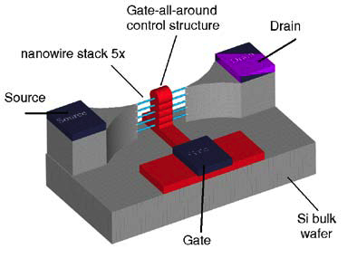
While chipmakers are struggling with the FinFET based chip production below 5 nm process nodes, Samsung has planned to opt for GAA (gate all around) architecture. Samsung’s GAA redesigns the transistor, making it more power-efficient and better-performing than the existing Multi Bridge Channel FET (MBCFET™) that utilize stacked nanosheets.
Samsung’s patented MBCFET™ is formed as a nanosheet, allowing for a larger current and simpler device integration. It allows to reduce the operating voltage below 0.75 V that had been extremely difficult with FinFET. This yields to 50% less power consumption or 30% more performance at 45% less chip area compared to 7 nm FinFET technology. Also, Samsung's GAA technology is compatible with current FinFET production line that means the today's fab running on mature process tools and methodology can be utilized for GAA transistors. Here is the infographic to learn more about how Samsung’s GAA is advancing the future of semiconductor technology.
Source: Samsung LINK
Written by : Abhishekkumar Thakur and Jonas Sundqvist
Using a new manufacturing technique, MIT researchers fabricated a 3-D
transistor less than half the width of today’s slimmest commercial
models, which could help cram far more transistors onto a single
computer chip. Pictured is a cross-section of one of the researchers’
transistors that measures only 3 nanometers wide.Credits Courtesy of the researchers: Published under a Creative Commons Attribution Non-Commercial No Derivatives license
[MIT News] Researchers from MIT and the University of Colorado have fabricated a 3-D transistor that’s less than half the size of today’s smallest commercial models. To do so, they developed a novel microfabrication technique that modifies semiconductor material atom by atom.
As described in a paper presented at this week’s IEEE International Electron Devices Meeting, the researchers modified a recently invented chemical-etching technique, called thermal atomic level etching (thermal ALE), to enable precision modification of semiconductor materials at the atomic level. Using that technique, the researchers fabricated 3-D transistors that are as narrow as 2.5 nanometers and more efficient than their commercial counterparts.
The 64th IEDM conference will be held December 1-5, 2018 in San Francisco (LINK). This year Samsung will give insights to their 3nm CMOS technology that will feature the so calle gate-all-around (GAA) transistors. The GAA is trasistors ar realized by having channels made from horizontal layers of nanosheets that are completely surrounded by gate structures.
Samsung has recently stated (LINK) that they have started wafer production on its new 7LPP node (FinFET). According to the press release the process uses EUV lithography technology and demonstrates that Samsung's Foundry can
follow its roadmap reaching down to 3 nm.
Samsung Foundry Roadmap as shown at SFF Japan 2018.
Samsung refers to this architecture as a Multi-Bridge-Channel architecture, and claims "that it is highly manufacturable as it makes use of ~90% of the company’s existing FinFET fabrication technology, requiring only a few revised photomasks" (LINK).
Paper #28.7, "3nm GAA Technology Featuring Multi-Bridge-Channel FET for Low-Power and High-Performance Applications," G. Bae et al, Samsung
Here is an interesting paper to be presented by Imec at the upcoming IEDM 2018 in San Fransisco. Imec has managed to stack the complete FinFET front end module on top of a "standard" bulk silicon FinFET Module demonstrating also good threshold
voltage tuning, reliability and low-temperature performance.
So just imagine if this would be used in high volume manufacturing - it would mean that all those ALD processes used in patterning and for the high-k metal gate module, spacers, local interconnect etc. etc. would come twice meaning a 2X need for ALD process chambers. And lets say you can run this twice - is there any reasons why you can´t run it yet another time? Woah!
Also as a note, Imec is here using a LaSiOx layer an a dipole inserted in the HKMG stack - presumably it is an ALD process since it will have to conformally coat this fins and ensure precise thickness control and uniformity.
So just enjoy seeing double - it is Friday!
Paper #7.1, “First Demonstration of 3D Stacked FinFETs at a 45nm Fin
Pitch and 110nm Gate Pitch Technology on 300mm Wafers,” A. Vandooren et
al, Imec
Highest-Density 3DS Stacked FinFETs: Imec researchers will report on
3D stacked FinFETs that have the tightest pitches ever reported in such
a stacked architecture – 45nm fin pitch and 110nm gate pitch. The 3D
architecture makes use of a sequential integration process yielding
tight alignment between very thin top and bottom Si layers. The
junction-less devices in the top layer were fabricated and transferred
using low-temperature (≤525ºC) processes to avoid performance
degradation, and a 170nm dielectric was used to bond the two wafers. The
top layer is so thin that the bottom layer could be patterned right
through it by means of 193nm immersion lithography, which connects the
two via local interconnect. The researchers evaluated various gate
stacks, ultimately choosing TiN/TiAl/TiN/HfO2 with a LaSiOx dipole
inserted into the stack. The combination demonstrated good threshold
voltage tuning, reliability and low-temperature performance.
At
left above is a cross-sectional electron microscope image of the
fabricated 3D stacked FinFETs along fins and across gates, showing the
tight alignment achieved by the top processed layers (Gate Li1, Li2)
toward the bottom layers. At right is a cross-sectional image of the
final devices across fins with the gates covering the fins.
“First Demonstration of 3D Stacked FinFETs at a 45nm Fin Pitch and 110nm
Gate Pitch Technology on 300mm Wafers,” A. Vandooren et al, Imec (IEDM 2018 Press kit)
Lam Research has published a tutorial on FinFETs basics that is very
interesting for anyone who likes to understands the basics of FinFETs:
Transistors are at the heart of our cherished electronics. Millions, or even billions, of these tiny switches go to work for us when we check our mobile phones, use our computers, start our automobiles, or play on our gaming consoles. But what exactly are transistors and how do they work? And how have they changed over the years? Here we take a look at some transistor fundamentals, including the operation of a field-effect transistor (FET), as well as the FinFET technology inflection that is enabling even smaller, more powerful semiconductor chips.
Readers of this blog may have noticed that I got a new hobby and that I´ve been looking into some etching (ALE) on the side. Here is some interesting new results in etching InP Fins for future CMOS by a chemical method "enabled by inverse metal-assisted chemical etching". All recently published by University of Illinois researchers in Silicon Semiconductors and in the IEEE ElectronDevice Letter below. (Thanks Nicklas Nilsson for sharing this one).
A cross-sectional microscope image of a fin transistor. The indium
phosphide semiconductor fin is overlaid with insulators and metals to
make a working transistor. Image by Yi Song (as published in Silicon Semiconductors)
Ultra-High Aspect Ratio InP Junctionless FinFETs by a Novel Wet Etching Method
Abstract:
Junctionless FinFETs with an array of ultra-high aspect ratio (HAR) fins, enabled by inverse metal-assisted chemical etching, are developed to achieve high on-current per fin. The novel device fabrication process eliminates dry etching-induced plasma damage, high energy ion implantation damage, and subsequent high-temperature annealing thermal budget, ensuring interface quality between the high-k gate dielectric and the HAR fin channel. Indium phosphide junctionless FinFETs, of record HAR (as high as 50:1) fins, are demonstrated for the first time with excellent subthreshold slope (63 mV/dec) and ON/OFF ratio (3 × 10⁵). Published in: IEEE Electron Device Letters ( Volume: 37, Issue: 8, Aug. 2016 )
Chipmakers are currently ramping up 16nm/14nm finFET processes, with 10nm and 7nm just around the corner. The industry also is working on 5nm. TSMC hopes to deliver a 5nm process by 2020. GlobalFoundries, Intel and Samsung are doing R&D for that node.
But 5nm technology presents a multitude of unknowns and challenges. For one thing, the exact timing and specs of 5nm remain cloudy. Then, there are several technical and economic roadblocks. And even if 5nm happens, it’s likely that only a few companies will be able to afford it.
“My current assumption is that 5nm
will happen, but it won’t hit high-volume manufacturing until after
2020,” said Bob Johnson, an analyst at Gartner. “If I were to guess, I’d
say 2021 to 2022.”
10 nm FinFET may start to ship as early as end of 2016. However, according to a recent article by Mark Lapedus (at Semiconductor Engineering) Bob Johnson, an analyst at Gartner, projects that 7nm could get pushed out to 2020. "This, in turn, could impact the potential timing of 5nm, if the industry
decides to move forward with the technology. “I assume 5nm will happen,
but not by 2020,” Johnson said, adding that a viable 5nm process may
not appear until the next decade, possibly 2023."
The slow down in scaling is not something new and has been seen for some time now. Above is a forecast presented at 2014 Semicon West with conclusions of the SEMI’s World Fab Forecast - Technology Node Transitions Slowing Below 32 nm. Her you can clearly see that the node transitions has paced slower since 28/32 nm. The question now is then if the pace will come to a halt.
The current 3 main options for 5nm logic FETs are :
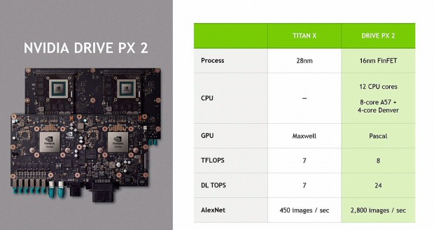
Recently we had Audi and Samsung announcing that ALD High-k DRAM volatile memory will be used in future joint electronics in Audi cars. At CES in Las Vegas Nvidia Corp.
unveiled a new, lunchbox-size super-computer for self-driving cars and
said Volvo Car Group will be the new device's first customer. Volvo
plans to install the device in 100 cars to be launched in 2017 as part
of a large-scale trial of autonomous driving technology in Göteborg,
Sweden. [Reuters]
Googling around I found what Logic is used and it seems to be 16 nm TSMC FinFET technology and then we should have round about 10 ALD process steps or maybe even more!
Nvidia Drive PX 2 (Bild:Nvidia/Screenshot: Golem.de). Since it says 16nm and not 14nm we can assume that the CPU is fabricated by TSMC in Taiwan.
Nvidia CEO Jen-Hsun Huang Keynote speaker at CES shows the Hardware module for Drive PX 2. (Bild: Nvidia)
This is how happy Zlatan Ibrahimovic was the first time he sat in his Volvo 2015 XC90 that he picked up in Paris Auto show from Volvo boss Håkan Samuelsson. Let´s hope Zlatan get the ALD upgrade as well.
Some ASM A412 Large Batch Furnaces form inside a TSMC 300mm Fab (Photo : Copyright® Taiwan Semiconductor Manufacturing Company Limited 2010-2016, All Rights Reserved. )
Screendump showing the ultimate goal of integration III/V vertical nanowire transistors.
"Driven by the growing demand for increased communication and increased
mobile and server data traffic, CMOS technologies will require
continuous innovations in the field of ultra-low power operation,
performance and density scaling. And this at an affordable cost. In this
movie, we visualize the evolution of a FinFET architecture into the
next technology generations: from tall Si fins and source/drain
stressors over "
VLSI 2015 is going on and there are a lot of interesting information flowing from there and especially on the future of CMOS scaling. Here is a good article on what´s next after FinFET by Peter Clarke. He is claiming that Silicon Nanowires is the most probable path, i.e., not III/V on silicon: Silicon Nanowire Remains Favorite to Replace FinFET. The article is based on the published information and opinions from ARM, Imec, and Prof. Asenov and tries to give insights to some of the major questions and possible issues:
Vertical or Lateral?
With or without EUV?
What Material?
Below some of the statements made by the experts in the article by Peter Clarke. Please do read the article for the full story here (IHS Electronics360).
Prof. Asen Asenov of Glasgow University and CEO of Gold Standard Simulations
Asenov says, "I do not think that there is a real alternative to NWTs. They are a natural progression to FinFETs. Think of it like this: MOSFET—gate on the side of the channel; FinFET—gate on three sides of the channel; NWT or gate all around—gate on four sides of the channel." In a word, ultimate control of the current.
Aaron Thean, logic research director at IMEC.
"At IMEC we look at silicon, silicon-germanium and III-V channel materials but the preference is silicon." Other materials suffer from immaturity. "You have to ask what is the value proposition for these materials? SiGe improves mobility but there are issues of reliability. It is very difficult to passivate the surface." So for Thean, at least, progress is likely to be based in silicon with first-scaled FinFET. That means a taller fin, then movement to lateral nanowire transistors. But it still needs some level of innovation, he says.
Lucian Shifren, principal engineer at ARM.
"Gate-all-around silicon is most likely for a 'real' 7nm," Shifren says. He adds that the nominal 7nm would likely be a pseudo-scaled FinFET and that the nominal 5nm process would be gate-all-around.
The Technology roadmap as presented recently by Imec at the EWMOVPE workshop in Lund, Sweden.
As the major portion of the industry adopts FinFETs as the workhorse transistor for 16nm and 14nm, researchers worldwide are looking into the limits of FinFETs and potential device solutions for the 7nm node and beyond. Two approaches, namely Gate-All-Around Nanowire (GAA NW) FETs, which offer significantly better short-channel electrostatics, and quantum-well FinFETs (with SiGe, Ge, or III-V channels), which achieve high carrier mobility, are promising options.
For the first time, imec demonstrated the integration of these novel device architectures with state-of-the-art technology modules like Replacement-Metal-Gate High-k (RMG-HK) and Self (Spacer)-Aligned Double-Patterned (SADP) dense fin structures. By building upon today’s advanced FinFET technologies, the work shows how post-FinFET devices can emerge, highlighting both new opportunities as well as complexities to overcome.
Imec and its technology research partners demonstrated SiGe-channel devices with RMG-HK integration. Besides SiGe FinFET, a unique GAA SiGe nanowire channel formation during the gate replacement process has been demonstrated. The novel CMOS-compatible process converts fin channels to nanowires by sacrificial Si removal during the transistor gate formation. The process may even enable future heterogeneous co-integration of fins and nanowires, as well as Si and SiGe channels. The work also demonstrates that such devices and their unique processing can lead to a drastic 2x or more improvement in reliability (NBTI) with respect to Si FinFETs.
Moreover, imec demonstrated Si GAA-NW FETs based on SOI with RMG-HK. The work compares junction-based and junction-less approaches and the role of gate work function for multi-Vt implementations. New insights into the improved reliability (PBTI) with junction-less nanowire devices have been gained.
Extending the heterogeneous channel integration beyond Si and SiGe, imec demonstrated for the first time strained Ge QW FinFETs by a novel Si-fin replacement fin technique integrated with SADP process. Our results show that combining a disruptive approach like fin replacement with advanced modules like SADF-fin, RMG-HK, direct-contacts can enable superior QW FinFETs. The devices set the record for published strained Ge pMOS devices, outperforming by at least 40% in drive current at matched off-currents.
Imec’s research into advanced logic scaling is performed in cooperation with imec’s key partners in its core CMOS programs including GLOBALFOUNDRIES, INTEL, Micron, Panasonic, Samsung, SK hynix, Sony and TSMC.
Nanowire transistors are the most likely successor to finfets and will scale to 5nm, says Professor Asen Asenov, Professor of Electrical Engineering at Glasgow University and CEO of Gold Standard Simulations (GSS) which specialises in the predictive simulation of nano-CMOS devices including statistical variability and reliability.
”While 16/14nm FinFETs are about to enter volume production at the major foundries, the next generation transistors suitable for 7nm CMOS and below are already on the drawing board,” says Asenov, “one of the best candidates “Gate all around” transistors, better known as nanowire transistors (NWT), have superior scaling properties compared to FinFETs and can be scaled to channel lengths of approximately 5nm. ”
Mobile charge distribution in a NWT with different cross-sections suitable for 7nm CMOS technology. Due to quantum mechanical confinement effects ‘strange’ patterns determine the Source' Drain' Gate' Spacer' Channel' positions of the current flow in the nanowire cross-section (Picure from GSS).
2016 will be another growth year for OEM stocks and Atomic Layer Processing. In a report recently published by JP Morgan, analysts predicted another growth year in 2016 for Semiconductors stocks, driven by technology transitions in memory and 10nm FinFET. So this is good news for all Tier 1 OEMs with a number of ALD and ALE technologies in the game.
"In general, we see capital intensity increasing by 10-15% on a per wafer basis when transitioning from 14nm/16nm FinFET to 10nm FF and by 15+% when transitioning to 20nm and below DRAM / 3D NAND. The number of critical patterning layers is increasing dramatically – in the foundry/logic segment, the number of critical layers is increasing by over 3x going from 28 nm node to the 10nm node…a significant increase," the analysts added.
Below is an overview of some of the ALD and ALE technologies offered by the leading OEMs. It is ion sense complete yet so please let me know what is missing (jonas.sundqvist@baldengineering.com).
LAM Research
LAM Research reported in 2014 that "The latest in Lam's market-leading tungsten deposition product line, the ALTUS Max ICEFill system controls variability by providing void-free fill of the geometrically complex 3D NAND wordlines. Using a proprietary filling technique, the new system creates the tungsten wordlines with an inside-out atomic layer deposition (ALD) process. The ICEFill process completely fills the lateral (horizontal) lines without any voids, while at the same time minimizing deposition in the vertical channel area. As a result, both electrical performance and yield are enhanced."
Lam’s ALTUS systems combine CVD and ALD technologies to deposit the highly conformal films needed for advanced tungsten metallization applications (http://www.lamresearch.com/products/deposition-products).
Lam's new ALE capability on the 2300 Kiyo F Series conductor etch system provides both the productivity and technology needed. The product leverages fast gas switching and advanced plasma techniques in the reactor to boost throughput, while dynamic RF bias enables the directional etching required to remove material in high aspect ratio (deep and narrow) features. As the latest offering in Lam's market-leading Kiyo family, the 2300 Kiyo F Series system continues to provide superior uniformity and repeatability enabled by a symmetrical chamber design, advanced electrostatic chuck technology, and independent process tuning features.
Shallow trench isolation
Source/drain engineering
High-k/metal gate
FinFET and tri-gate
Double and quadruple patterning
3D NAND
To learn how atomic layer deposition (ALD) and atomic layer etch (ALE) processes work, watch this video from LAM Research (www.youtube.com).
Applied Materials
CENTURA® ISPRINT™ TUNGSTEN ALD/CVD - The Applied Centura iSprint Tungsten ALD/CVD system provides complete contact/via fill for structures with aspect ratios ranging from 4:1 to 7:1 and extends the capability of tungsten technology to 20nm/16nm for logic and memory applications.
The iSprint system also delivers high throughput and low cost of consumables with an optimized ALD chamber design featuring a proprietary rapid gas delivery system and small chamber volume that enable fast, effective gas purging that uses less gas (www.appliedmaterials.com).
CENTURA® INTEGRATED GATE STACK - The system consists of an ALD HfO2 (hafnium oxide) deposition chamber and specialized chambers for interface layer oxide formation, post high-k nitridation, and post-nitridation anneal
The Centura Integrated Gate Stack system with ALD high-k chamber technology for 22nm and below uses Applied’s production-proven Centura Gate Stack platform to deliver the complete high-k process sequence in a controlled high vacuum environment without an “air break” (www.appliedmaterials.com).
Steven Hung, Ph.D. who specializes in integrating ALD into the transistor manufacturing process, dives deep into the chip to show what tomorrow's transistors look like, how they work, and how Applied can help the industry meet the challenges of fabricating these ultra-tiny structures to make faster, more power-efficient microchips (www.youtube.com).
Tokyo Electron
Tokyo electron has a number of ALD technologies and are very strong in batch processing that is used to large extent in DRAM production to get the cost per wafer down since DRAM is a commodity product.
TEL Formula - Mini batch, thermal processes including ALD for High-k, SiO2, SiN.
TEL INDY Plus - Large batch, thermal processes including ALD for High-k, SiO2, SiN.
TEL INDY IRad - Large batch, PEALD for ultra low temperature SiO2 and SiN.
TEL NT333 - Single wafer cluster tool for high t-put SiO2.
TEL INDY Large batch furnace for thermal processing and ALD (www.tel.com)
The NT333 applies inherent ALD concepts against conventional ALD processing to address the critical performance needs imposed by aggressive geometries. The NT333 can effectively deposit with a very tight thickness control, a range of less than 1A, while maintaining a productivity of 100+ wafers per hour. With a very unique reactor design, each of the ALD duty cycles enables the NT333 to deliver the high film quality which is typically compromised at low temperature regimes (<400C). (www.tel.com)
ASM International
ASM's ALD technologies, includes thermal ALD (Pulsar) for FinFET high-k metal gate stacks, and various applications of Plasma Enhanced ALD (Emerald) as an enabler for low temperature processing such as multiple patterning on resist and deposition of doped silicon oxide for solid state doping of FinFETs.
ASM’s Pulsar uses ALD to deposit the high-k dielectric materials required for advanced CMOS transistor gates and other applications. Pulsar is the benchmark ALD high-k tool for the industry. It was the first ALD system to be used for high-volume production at advanced customers for high-k metal gate transistors (www.asm.com).
EmerALD XP is a process module designed to deposit thin conformal metal and dielectric layers by atomic layer deposition (ALD) used for advanced CMOS gate stacks and other applications (www.asm.com).
Eagle XP8 is a high productivity 300mm tool for PEALD applications. The Eagle XP8 PEALD system can be configured with up to four Dual Chamber Modules (DCM), enabling eight chambers in high volume production within a very compact footprint (www.asm.com).
High-k für Alle - A very nice overview of the High-k/Metal Gate transistors that enabled the mobile revolution that we have enjoyed in the last years. Atomic Layer Deposition is definitely part of this revolution amongst other semiconductor manufacturing techniques. Originally published for the Advanced Semiconductor Manufacturing Conference (ASMC), 2014 25th Annual SEMI (19-21 May 2014) by Dick James at Chipworks. Many of these has been published earlier by Chipworks and this paper covers them all and is therefore a very good overview for anyone into high-k and modern transistors.
Abstract: 2007 saw the introduction of the first high-k/metal gate (HKMG) devices into the marketplace. This marked the return of metal-gate technology on silicon for the first time since polysilicon gates became ubiquitous in the early 1970s. Intel was the first to use high-k/metal gate in its 45-nm product. Other leading-edge manufacturers have now launched HKMG products in both gate-first and gate-last forms at the 28-nm node, and we have seen the first HKMG finFET products from Intel. In the near future we also expect to see the first 20-nm foundry products come onto the market. Chipworks, as a supplier of competitive intelligence to the semiconductor and electronics industries, monitors the evolution of chip processes as they come into commercial production. Chipworks has obtained parts from the leading edge manufacturers, and performed structural analyses to examine the features and manufacturing processes of the devices. The paper discusses some of the different transistor structures we have seen during the evolution of the HKMG technology, and examines the variety of 32/28-nm parts that have been introduced. We will also show more details of the Intel 22-nm finFETs.
The paper covers eight of the transistor structures that have made it into production in the last two years. HKMG processes in the industry have bifurcated into gate-first (IBM, GLOBALFOUNDRIES, Samsung) and gate-last (Intel, TSMC), with different implementations within each group. At the 20-nm node the majority of processes will migrate to planar gate-last, with IBM staying with the gate-first technology for their in-house products. Below 20-nm, we will start to see other finFET processes come into production
VIDEO : An overview on Atomic Layer Etching (ALEt) created for Stanford Nanomanufacturing Class July 2014. Thanks Annina at ALDPulse.com for sharing this!
Screendump - explaining self aligned double pattering (SAPD) and cration of silicon fins for leading edge FinFETs.
Atomic Layer Etch Finally Emerges - is a interesting blog post by Mark LaPedus (Executive Editor for manufacturing at Semiconductor Engineering) that you should really read if you want some insight into why we need ALE and why it has been difficult to develope this etch technique.
After nearly two decades of being confined to R&D labs, equipment makers are placing big bets on this next-gen plasma etch technology.
[...]
Lam’s Lill agrees that ALE will not replace RIE. “We will offer both technologies in one reactor,” Lill said. “We think they will be complementary for certain applications. But we are already seeing the transition (to ALE) in certain applications.”
ALE could be used for 3D NAND, sub-20nm DRAMs and finFETs, but there are still some challenges before ALE is running in the production fab. “There are still three grand challenges left,” Lill said. “One is that there are no secondary unintended reactions for ALE. For example, we don’t want extreme UV radiation in the reactor. Second, we want the unit steps to be discrete. And finally, we need self-limiting single unit steps. They are very difficult to find.”
The FinFET process is a way to stack additional transistors onto the silicon, thereby making faster and more power-efficient chip. For an explainer on the manufacturing process, watch the video below. The term FinFET was coined by University of California, Berkeley researchers (Profs. Chenming Hu, Tsu-Jae King-Liu and Jeffrey Bokor) to describe a nonplanar, double-gate transistor built on an SOI substrate. The distinguishing characteristic of the FinFET is that the conducting channel is wrapped by a thin silicon "fin", which forms the body of the device. The Wrap-around gate structure provides a better electrical control over the channel and thus helps in reducing the leakage current and overcoming other short channel effects. In current usage the term FinFET has a less precise definition. Among microprocessor manufacturers, AMD, IBM, and Freescale describe their double-gate development efforts as FinFET development whereas Intel avoids using the term to describe their closely related tri-gate architecture. In the technical literature, FinFET is used somewhat generically to describe any fin-based, multigate transistor architecture regardless of number of gates. In 2012, Intel started using FinFETs for its future commercial devices. In September 2012, Globalfoundries announced plans to offer a 14-nanometer process technology featuring FinFET three-dimensional transistors in 2014. The next month, the rival company TSMC, announced start early or "risk" production of 16 nm FinFETS in November 2013.[adopted from Wikipedia]
Recently Samsung and Globalfoundries announced an agreement between the two companies would see Samsung develop a 14nm process node and license it to Globalfoundries.
Screendump showing the ALD high-k dielectric and TiN metal gate wrapping the fin conformally.
This Globalfoundries factory near Albany, New York, will adopt a production process developed by Samsung. Kelvin Low, senior director of marketing for Samsung's North American foundry operations, said its 14-nanometer process is already being used to produce some customer chips in small quantities. It predicts volume production by the end of 2014 using the process, which will be introduced at two factories in South Korea as well as Austin. [Source WSJ]


%20(1).png)