
Register now for a FREE #ACSScienceTalks #VirtualEvent with Assoc Editor discussing "The Industrial Ecosystem of Si Chips & Atomic Layer Deposition as a Key Nanofabrication Technology."  brnw.ch/21wC0I4
brnw.ch/21wC0I4 


%20(1).png) brnw.ch/21wC0I4
brnw.ch/21wC0I4 Champion 23.7% efficient perovskite-PERC tandem cell was achieved.
The developed thermal atomic layer deposition (ALD) process for NiO is reported.
ALD NiO was added to an ITO/SAM recombination junction to improve the device yield.
Dutch researchers at TNO and TU Eindhoven have achieved a notable breakthrough in solar cell technology by creating a monolithic perovskite-PERC tandem solar cell with a remarkable 23.7% efficiency. The innovation lies in a new tunnel recombination junction (TRJ) design that includes indium tin oxide (ITO), carbazole (2PACz), and a nickel(II) oxide (NiO) layer. Unlike conventional TRJs, the addition of NiO significantly reduces electrical issues in the perovskite top cell.

(a) HAADF-scanning transmission electron microscopy (TEM) image of a tandem cell using ITO/NiO/2PACz. (b) Compositional line profiles at the interface ITO/NiO/SAM extracted from an EDX elemental mapping. Note that the figure is rotated 90°.
By using atomic layer deposition (ALD), the team improved the uniformity of the self-assembled monolayer (SAM) in the TRJ structure. This new solar cell design includes a perovskite absorber, electron transport layers, an ITO electrode, a silver (Ag) metal contact, and an antireflective coating.
Comparing their creation with a reference cell, the researchers found the novel TRJ-based cell achieved an efficiency of 23.7%, slightly below the reference cell's 24.2%. However, the novel design's uniform coverage of SAM and consistent efficiency across different devices within and between batches makes it promising for large-scale production.
Published in Solar Energy Materials and Solar Cells, this research opens doors for improved perovskite-PERC tandem solar cell technology using ALD NiO.
Atomic layer deposition of NiO applied in a monolithic perovskite/PERC tandem cell - ScienceDirect
Trelleborg Sealing Solutions, a leading player in engineering solutions, is making waves at Semicon Taiwan 2023 by showcasing its cutting-edge engineering capabilities and an expanded range of semiconductor sealing solutions. The event, hosted at the Taipei Nangang Exhibition Center, features Trelleborg's booth highlighting their latest additions to the Isolast PureFab FFKM material range, a significant advancement in semiconductor seal technology.

At the forefront of their display is the Isolast PureFab JPF40, an ultra-high temperature perfluoroelastomer (FFKM) designed for demanding subfab applications and thermal processes. This includes pivotal processes such as rapid thermal processing (RTP) and atomic layer deposition (ALD), crucial for semiconductor manufacturing. This material boasts unparalleled compression set performance within a wide operating temperature range, ensuring airtight seals in critical processes even at extreme temperatures reaching +300°C. The remarkable capability to withstand peak application temperatures exceeding +325°C makes it a game-changer in the semiconductor industry.
Ethan Huang, the Semiconductor Segment Manager at Trelleborg Sealing Solutions, emphasized the vital role of reliable sealing solutions in safeguarding semiconductor processes against escalating temperatures and aggressive chemical agents. The Isolast PureFab JPF40 and other offerings within the PureFab range are meticulously engineered to address the unique challenges posed by semiconductor environments.
Furthermore, Trelleborg's expertise extends to predictive engineering through finite element analysis. This innovative approach aids in modeling compression set data, allowing engineers to more accurately estimate the usable lifetime of seals during design and production. This predictive technology is a significant leap forward, enabling enhanced seal longevity assessments.
A standout in their exhibition is the Isolast K-Fab Flange Seal, designed for critical subfab applications and capable of withstanding temperatures up to +327°C, dependent on material selection. The seal's versatility in material options, including Isolast FFKM, PureFab FFKM, and PureFab Fluoroelastomer (FKM), makes it adaptable to various requirements.
An interesting focus lies on Trelleborg's contributions to atomic layer deposition (ALD). Their materials, like Isolast PureFab JPF22, exhibit remarkable chemical compatibility with wet process chemicals, steam, and amine-based ALD precursors. This makes them well-suited for ALD applications, which are vital to modern semiconductor fabrication processes.
In addition to their product lineup, Trelleborg also presents the Turcon Variseal NW, showcasing their prowess in spring-energized seals for extreme environments. This seal operates across an extensive temperature range and excels in both wear resistance and friction characteristics.
Semicon Taiwan 2023 provides a platform for Trelleborg Sealing Solutions to not only showcase their groundbreaking products but also to engage with industry professionals about their specific sealing needs. The event highlights the convergence of innovative engineering and the semiconductor industry's evolving demands.
South Korea's SK Hynix Inc. has orchestrated a substantial resurgence in the DRAM chip sector during Q2, propelling itself back to the second-largest global position and surging ahead of Micron Technology Inc., which now stands third. The chipmaker achieved a nearly 50% surge in DRAM shipments, propelling its revenue to $3.44 billion in the April-June period. Notably, SK Hynix excelled in DDR5 and HBM chip shipments, products with higher average selling prices (ASPs) than standard commodity DRAM items, thus enhancing its ASP growth by 7-9% compared to the previous quarter. In contrast, market leader Samsung Electronics experienced a 7-9% ASP drop while retaining its top position, and third-place Micron sustained relatively stable ASP with DDR5 shipments. The overall DRAM industry marked a 20.4% QoQ revenue increase in Q2, signaling a potential turnaround in the sector.
SK Hynix leads DRAM industry’s Q2 revenue rebound, retakes No. 2 spot - KED Global
In a recent report by SEMI, in collaboration with TechInsights, the global semiconductor industry shows signs of emerging from its downcycle, with a projected recovery expected in 2024. The report highlights that the third quarter of 2023 is anticipated to witness a healthy 10% quarter-on-quarter growth in electronics sales, while memory IC sales are set to achieve double-digit growth for the first time since the downturn began in 2022. Although headwinds persist in the semiconductor manufacturing sector during the latter half of 2023, a rebound is on the horizon.

Inventory drawdowns at integrated device manufacturer (IDM) and fabless companies are forecasted to keep fab utilization rates lower than those seen in the first half of 2023. Despite this, positive trends are noted in capital equipment billings and silicon shipments, stemming from government incentives and robust equipment sales backlogs.
Market indicators suggest the semiconductor industry reached its nadir by mid-2023, commencing a path to recovery, setting the stage for growth in 2024. All segments are predicted to witness year-over-year increases in 2024, with electronics sales projected to surpass their 2022 peak.
Clark Tseng, Senior Director of Market Intelligence at SEMI, pointed out that the gradual demand recovery might extend the timeline for inventory normalization until the end of 2023, leading to temporary reductions in fab utilization rates. Nevertheless, semiconductor manufacturing is expected to hit its bottom in Q1 2024.
Boris Metodiev, Director of Market Analysis at TechInsights, highlighted the resilience of equipment sales and fab construction despite the broader downturn. He attributed this trend to government incentives driving new fab projects and strong backlogs supporting equipment sales.
Original Source: SEMI https://www.semi.org/en/news-resources/press-releases/2023/08/global-semiconductor-industry-on-track-for-2024-recovery-but-near-term-headwinds-remain-semi-reports


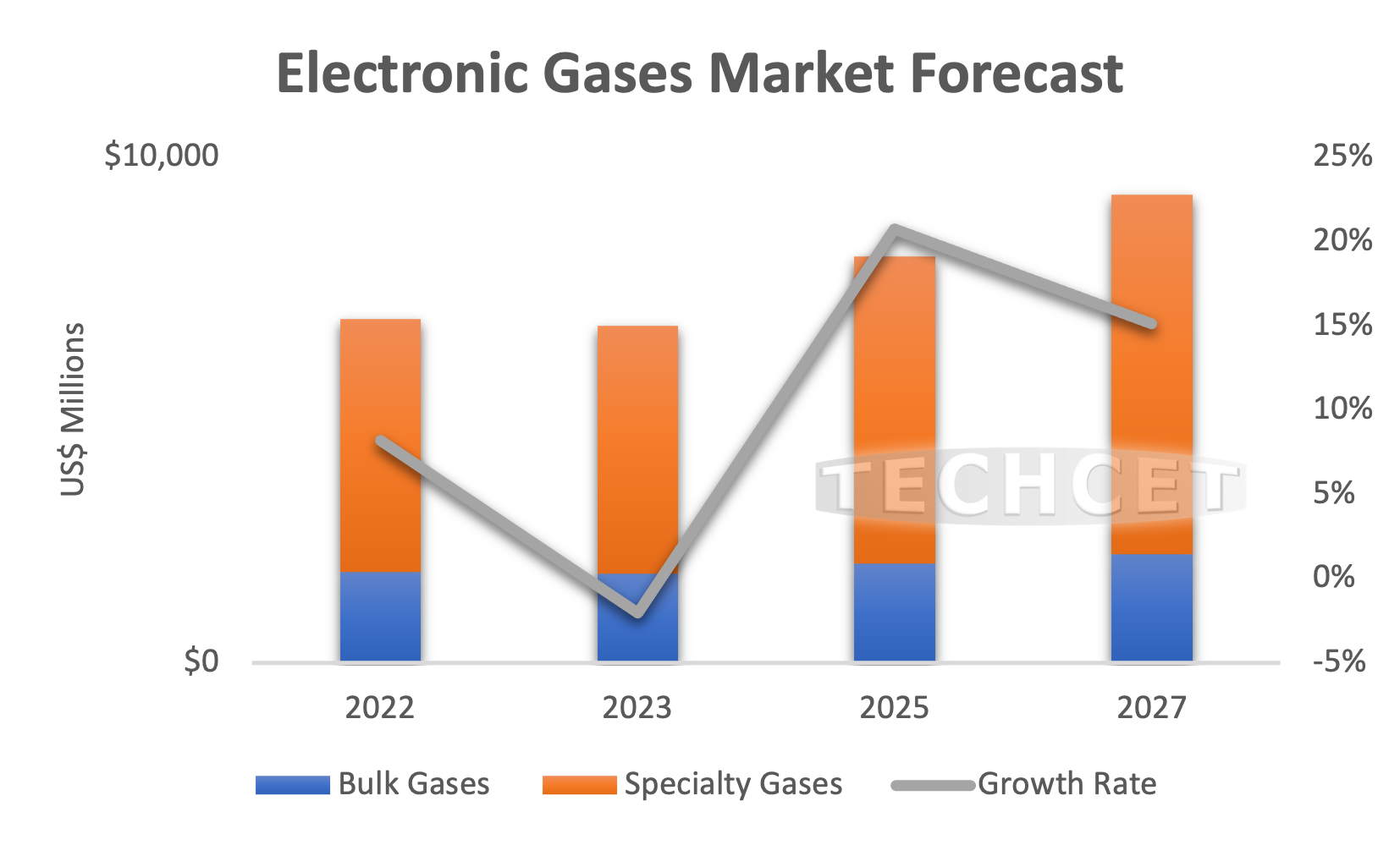
Germany-Based EMD Electronics Expands Schuylkill County, Pennsylvania, Operations - Area Development EMD Electronics, the North American electronics business of Merck KGaA, plans to expand its operation and establish a semiconductor specialty gasses manufacturing facility in Schuylkill County, Pennsylvania. The $300 million project is expected to cr www.areadevelopment.com |
In the dynamic landscape of materials science and technology, Swiss Cluster emerges as a pioneering force with its cutting-edge Atomic Layer Deposition (ALD) solutions. Founded by a team of experts hailing from the Swiss Federal Institute for Material Science & Technology (Empa) in Thun and Bern University of Applied Sciences, Swiss Cluster has swiftly carved a niche for itself in the field. The company's commitment to innovation and precision is evident in its diverse range of ALD products, each tailored to meet the demands of various industries and applications.
Swiss Cluster's journey began in 2019, and it officially registered as a company in November 2020. The driving force behind Swiss Cluster's success lies in the collective expertise of its team, which encompasses researchers and engineers specializing in thin films deposition techniques, vacuum and plasma deposition technologies, and materials characterization. This robust foundation has paved the way for the creation of three exceptional ALD products that are reshaping the way coatings are applied to 3D objects.

The SC Optima Series stands as a testament to Swiss Cluster's commitment to innovation and efficiency. Designed as the next generation of large batch systems for ALD, this series embodies the perfect synergy of precision, speed, and uniformity. Boasting a patent-pending chamber, the SC Optima Series can seamlessly adapt to various 3D parts and coating materials. Its exceptional coating homogeneity and record process speeds are achieved through the elimination of traditional barriers like transfer arms, thanks to the single chamber approach. This innovation not only streamlines loading and unloading but also facilitates rapid temperature control, optimizing the entire process from start to finish.
The SC-1 redefines what's possible in coating technologies by combining ALD with Physical Vapor Deposition (PVD). This groundbreaking modular system eliminates the need for vacuum breaks, minimizing downtime and maximizing throughput. The SC-1's ability to seamlessly integrate ALD and PVD techniques within a compact framework allows for the fabrication of multinanolayered coatings. This approach improves coating quality, stability, and material properties, making it a powerful tool for industries requiring tailored functionalities and properties. The SC-1's flexibility, scalability, and quality interfaces between different layers open doors to novel materials and applications.
For those focused on research, development, and small-scale production, the SC Qube offers an innovative solution. With its ALD batch system, the SC Qube caters to coating various 3D parts. The system's scalable chamber can be configured to fit different types and sizes of objects while delivering exceptional coating homogeneity. The ability to integrate the SC Qube into cleanroom environments or glovebox units, along with its easy front loading and custom-made holders, makes it a versatile choice for various applications. Rapid processing, precision, and adaptability define the SC Qube's contribution to the world of coatings.
Swiss Cluster's trio of ALD products represents a journey of expertise, innovation, and a commitment to enhancing the way materials are coated. From large batch systems to integrated solutions and research-focused offerings, Swiss Cluster's ALD products cater to the unique needs of different industries. As the company continues to push boundaries and refine coating technologies, its impact on diverse sectors, from electronics to medical applications, remains profound. Swiss Cluster's dedication to revolutionizing research and production processes paves the way for novel and better materials that shape our technological future.
Taiwan Semiconductor Manufacturing Co. (TSMC) has achieved a significant milestone in its Arizona manufacturing venture by installing its inaugural extreme ultraviolet lithography (EUV) machine. This advanced machine, procured from Dutch semiconductor equipment leader ASML Holding NV, is a pivotal asset for TSMC's future high-end chip production endeavors.
EUV technology is a critical aspect of semiconductor fabrication, facilitating the printing of intricate designs on microchips significantly smaller than a human hair. TSMC's achievement underscores its commitment to innovation and technological leadership.
While the installation of the EUV machine marks a remarkable accomplishment, TSMC acknowledges that the setup of the new fab in Arizona involves numerous additional tasks. The company emphasized the need for approximately 2,000 skilled workers to handle the installation of various equipment pieces and services in the complex. This requirement stems from TSMC's unique tool configurations and specifications.
TSMC, recognized as the world's largest contract chip manufacturer, is channeling substantial investments amounting to $40 billion into constructing two wafer fabs in Phoenix. The first facility will employ the advanced 4-nanometer process, while the second, already under construction, will utilize the more sophisticated 3-nanometer process. This latter technology has already entered mass production in Taiwan.
The presence of skilled workers has been a contentious topic linked to the Arizona project. TSMC Chairman Mark Liu explained that a deficiency in experts capable of properly installing equipment at the Arizona site has led to a delay in mass production, now projected for 2025 rather than late 2024.
However, TSMC's approach to addressing this shortfall has sparked debates. The company's bid to bring in around 500 Taiwanese workers on temporary E-2 visas has faced resistance from local unions, who assert that prioritizing American jobs is paramount, especially considering the significant subsidies TSMC seeks under the CHIPS and Science Act. This legislation, signed by President Joe Biden, encourages semiconductor investments in the United States.
US Senator Mark Kelly of Arizona emphasized that the visa applications will be evaluated in accordance with established laws and procedures. As TSMC navigates these challenges, its progress in Arizona remains a focal point in the semiconductor industry's dynamic landscape.
TSMC installs first EUV machine in U.S.; job opening ads posted - Focus Taiwan
DSA has emerged as a groundbreaking technique for mass-producing micro to nano devices and materials with precision and efficiency. This method harnesses the inherent properties of materials to assemble them into intricate structures, revolutionizing manufacturing processes across various industries.
DSA leverages block co-polymer morphology to create patterns, enhancing feature control and shape accuracy. This involves guiding the assembly of micro and nano particles to achieve desired structures, made possible by the precise control of surface interactions and polymer thermodynamics. The key advantage of DSA is its ability to create structures at remarkably small scales, enabling advancements in diverse fields.
In the semiconductor industry, DSA offers a new perspective on lithography challenges. Despite initial setbacks, DSA is being revisited to address critical issues such as stochastic defects in extreme ultraviolet (EUV) lithography. These defects, which can contribute significantly to patterning errors, have led semiconductor manufacturers to explore DSA as a solution to rectify these problems. Notably, DSA is not replacing traditional methods but rather enhancing them. It is being integrated with existing manufacturing processes to enable increased resolution and precision, all while reducing costs.
However, challenges persist in integrating DSA into high-volume manufacturing. Defect control remains a primary concern, as the technology strives to meet industry standards of minimal defectivity. Common defects include line bridging, collapse, bubbles, and dislocations. Efforts are ongoing to optimize annealing temperature, etching methods, and film thickness to reduce these defects. Another challenge is the complexity of pattern inspection, which demands accurate metrology methods. Researchers are exploring machine learning-based approaches to automate the inspection process and achieve higher throughput.
Despite these challenges, DSA is being applied to various applications beyond semiconductors. Tissue engineering benefits from the precision of directed assembly, enabling the controlled organization of cells into desired micro-structures. In nanotechnology, DSA facilitates the creation of precise nanostructures, leading to advancements in areas such as graphene nanoribbon arrays and thin-film quantum materials.
Revolutionizing EUV Lithography with Directed Self-Assembly (DSA)
EUV lithography has revolutionized semiconductor manufacturing but comes with its share of challenges, particularly in addressing line roughness and stochastic defects. DSA has now gained attention as a potential game-changer to tackle these issues in EUV lithography.
Recent research from Imec sheds light on the promising synergy between EUV and DSA in overcoming lithography challenges. In the study titled "EUV Lithography Line Space Pattern Rectification Using Block Copolymer Directed Self-Assembly: A Roughness and Defectivity Study," led by Julie Van Bel and team, the researchers explored the combination of DSA with EUV. Their findings indicate that this integration surpasses DSA processes based on Immersion lithography, offering lower line width roughness and freedom from dislocation defects.
Another study, "Mitigating Stochastics in EUV Lithography by Directed Self-Assembly," led by Lander Verstraete and collaborators, delved into the application of DSA to mitigate stochastic defects in EUV processing.


For contact arrays, the combination of EUV and DSA demonstrates improved Local Critical Dimension Uniformity (LCDU) and Pattern Placement Error. This advancement also enables the use of a lower dose, contributing to enhanced precision and efficiency in semiconductor manufacturing.
Imec's research underscores the potential of DSA to revolutionize EUV lithography by addressing line roughness and stochastic defects. The successful integration of EUV and DSA holds the promise of enhancing semiconductor manufacturing processes, achieving higher precision, and enabling the production of advanced devices with improved quality. As researchers continue to refine these methods, the collaboration between EUV and DSA is set to shape the future of lithography and microfabrication.
In conclusion, DSA is revitalizing micro and nano fabrication by offering accurate and efficient methods for mass production. While challenges like defect control and metrology persist, DSA's potential to shape the future of industries such as semiconductors, biomedicine, and nanotechnology is undeniable. As research continues to refine DSA processes and overcome hurdles, its role in advancing technology and innovation is set to expand further.
Directed Self-Assembly Finds Its Footing (semiengineering.com)
A paradigm shift is sweeping the power semiconductor landscape, with silicon carbide (SiC) emerging as the frontrunner. Driven by EV adoption and cost parity with silicon, SiC's ascendancy is reshaping the market. Thousands of SiC-based power semiconductor modules are already enhancing EV functions such as charging and conversion. SiC MOSFETs are supplanting silicon-based IGBTs, doubling power density and ramping switching speeds while downsizing form factors. This transformation hinges on SiC modules achieving price parity with silicon alternatives, fostering supply alliances and new SiC fabs. SiC modules play a pivotal role in the transition to 800V batteries, boosting EV adoption through faster charging and reduced costs. Despite challenges, analysts anticipate substantial SiC growth, particularly in automotive applications. This evolutionary journey towards energy-efficient power is projected to culminate in a $6.3 billion SiC power semiconductor market by 2027.
In the pursuit of advancing silicon carbide (SiC) technology, a suite of innovative wafer process tools is being employed. These tools encompass high-temperature epitaxial growth exceeding 2,000°C, hot ion implantation, rapid thermal processing (RTP), and Atomic Layer Deposition (ALD). Noteworthy adaptations are underway in wafer grinding, chemical-mechanical polishing (CMP), as well as the formulation of abrasion-resistant polishing pads and slurries tailored for the rigid, fragile SiC substrate. The evolution also encompasses novel materials like strippers and cleaning formulations, addressing device requirements and sustainability considerations. These cutting-edge processes collectively exemplify the industry's determination to optimize SiC production, enhance its characteristics, and foster its integration into diverse applications, from electric vehicles to renewable energy systems.
Power Semis Usher In The Silicon Carbide Era (semiengineering.com)

Dutch semiconductor equipment leader ASM International NV has established a pioneering training center at the Southern Taiwan Science Park's Tainan branch to offer intensive training for over 100 engineers employed by its clients. This newly inaugurated facility is ASM's first training center in Taiwan and signifies a significant step in enhancing semiconductor expertise. With more than 50 percent global market share in atomic layer deposition (ALD), ASM's training center introduction aims to harness virtual reality technology for hands-on learning and precision semiconductor equipment mastery. The center is poised to propel innovation and foster synergies between Taiwan and the Netherlands, two pivotal players in the semiconductor industry.

The training center will leverage cutting-edge virtual reality technologies, allowing trainees to transcend conventional learning boundaries. The utilization of online courses coupled with virtual reality tools will empower engineers to grasp the intricate aspects of precision semiconductor equipment more effectively.
Guido Tielman, head of the Netherlands Office Taipei, highlighted the strategic collaboration between the Netherlands and Taiwan in shaping the global semiconductor landscape. He underscored the significance of this training center in fortifying ties and harnessing the immense business opportunities presented by the dynamic semiconductor sector.
This venture aligns with Taiwan's thriving semiconductor ecosystem, further enriched by the presence of other industry giants like ASML Holding NV, renowned for its extreme ultraviolet lithography (EUV) photolithography machines. The Netherlands, Taiwan, and ASM International are collectively poised to leverage their expertise to excel in the competitive global semiconductor market.
ASM International's state-of-the-art training center marks a pivotal moment in the advancement of semiconductor knowledge and technology. This strategic collaboration between the Netherlands and Taiwan is set to drive innovation, propel semiconductor advancements, and foster the development of highly skilled engineers, amplifying the capabilities of the global semiconductor industry.
Dutch IC equipment supplier opens training center in Tainan - Focus Taiwan
Nanexa AB, a pioneering pharmaceutical company, has unveiled a significant advancement in the realm of drug delivery. The company recently revealed exciting results from its Phase 1 study, designated NEX-20-01, which underscored the controlled release of lenalidomide in varying doses over a span of up to 21 days.
Atomic Layer Deposition (ALD) is a cutting-edge technique used in medical and pharmaceutical applications, particularly in the development of Nanexa's PharmaShell® technology. ALD's precision in depositing thin layers of materials plays a vital role in creating the controlled-release shell of PharmaShell®. This nanoscale engineering ensures accurate drug delivery, regulating release rates and optimizing therapeutic effects. PharmaShell® benefits from ALD's versatility, enhancing drug efficacy, minimizing side effects, and allowing tailored treatment plans. ALD's role in crafting PharmaShell® exemplifies its impact in advancing drug delivery systems, revolutionizing pharmaceutical care.

The study, conducted with great precision and care, involved nine healthy volunteers who were administered either one or two subcutaneous single injections of the innovative NEX-20A formulation. This formulation encompassed doses ranging from 15 to 35 mg of lenalidomide, with a maximum cumulative dosage of 50 mg. The outcome was nothing short of remarkable, as the observed pharmacokinetic data from the human participants correlated excellently with the projected exposure calculated from preclinical studies.
Central to the accomplishment was the remarkable release mechanism employed by Nanexa, known as PharmaShell®. This ingenious approach ensured a controlled and gradual release of the drug into the participants' bodies, creating a plasma curve that spanned an impressive 21 days. A critical observation from the study was the initial low release of the total dosage within the first day. This gradual release strategy plays a pivotal role in maintaining optimal levels of the drug in the bloodstream throughout the treatment period.
Equally encouraging was the confirmation that the total exposure of lenalidomide in the plasma—measured as the area under the curve (AUC)—escalated proportionally with the administered dose. This finding aligns with the expectations and demonstrates the efficacy of the PharmaShell® system in achieving the desired therapeutic outcomes.
Nanexa's CEO, David Westberg, expressed his enthusiasm regarding this groundbreaking achievement. "This is an important achievement for Nanexa, to once again demonstrate that we can predict the release profile of PharmaShell® in humans based on preclinical data," he shared. Westberg also revealed the company's forward-looking plans, stating, "We are now continuing to optimize the formulation and are ready to plan for the next clinical study of NEX-20 in patients. In that study, where we plan to increase the dose, we want to ensure that we will continue to minimize local reactions, and we see good results from preclinical studies on how this can be done."
Safety, of course, remains a top priority in such endeavors. Nanexa is committed to compiling comprehensive safety and tolerability data, which will be meticulously assessed following the final follow-up visits for the last dose group in October. Encouragingly, the study thus far has reported limited and transient injection site reactions, with no unexpected severe or systemic side effects. This bodes well for the continued development and progress of the NEX-20 project.
Nanexa's accomplishments in the controlled release of lenalidomide mark a significant milestone not only for the company but also for the entire field of pharmaceuticals. The ability to meticulously regulate the release profile of drugs while simultaneously minimizing undesirable side effects holds great promise for revolutionizing patient care and treatment outcomes. As Nanexa continues to pave the way with its innovative approach, the future of pharmaceuticals looks more promising than ever.
In a groundbreaking partnership, Extended Reality (XR) technology leader Imitera and semiconductor innovator AlixLabs are set to reshape the way industries collaborate and innovate. The collaboration aims to leverage the power of XR to enhance visualization and communication within AlixLabs' semiconductor manufacturing process.
Imitera's cutting-edge XR platform is poised to unlock a new era of collaboration for AlixLabs. By creating a virtual environment where teams can interact with atomic and molecular structures, XR technology enables live testing and seamless sharing of information. This revolutionary approach empowers teams to make decisions collaboratively, irrespective of geographical barriers.

Dr. Jonas Sundqvist, CEO of AlixLabs, expressed his amazement at the insights gained through the XR atomic level world. He likened the experience to being immersed in an IKEA ball bath as he and his team explored atomic-level structures virtually. The technology not only sparks imagination but also provides real-world benefits for dispersed teams, like AlixLabs', to engage as if they were physically present.
The collaboration between Imitera and AlixLabs exemplifies the transformative potential of XR technology. By addressing the demand for immersive, cost-effective, and user-friendly experiences, Imitera's XR solutions have the power to drive innovation across various industries. AlixLabs' groundbreaking semiconductor manufacturing technique coupled with Imitera's XR platform showcases a new way forward for industries to connect, visualize, and innovate.
The partnership between Imitera and AlixLabs isn't just about merging technologies; it's about merging minds. With XR technology as the bridge, teams can transcend traditional barriers and engage in a shared space that fosters creativity and informed decision-making. This collaboration marks a significant step toward revolutionizing industries and shaping the future of collaboration.
In a world where physical distances are no longer limitations, the synergy between XR and semiconductor innovation is a testament to human ingenuity. As these two worlds converge, the possibilities for cross-industry collaboration and discovery are boundless.

Episode Highlights:
**00:00 - Intro:** An introduction to the ALD technology and its rapid development over the past 50 years.
**01:33 - Suntola’s 1st Reactor:** Delving into Tuomo Suntola's original ALD reactor and its significance in kickstarting the technology's journey.
**03:15 - Suntola’s Patented Configurations:** Exploring the patented configurations of ALD reactors, including the technological advancements they brought about.
**07:38 - The First Commercial Reactor:** Reflecting on the emergence of the first commercial ALD reactor and its role in driving the technology towards industrial applications.
**10:50 - Plasma, Please:** Examining the introduction of plasma into ALD reactors and how it enhanced film deposition processes.
**15:20 - Powder ALD Reactors:** Investigating the utilization of powder-based ALD reactors, which added a new dimension to thin film deposition.
**20:37 - Reintroduction of Spatial ALD:** Discussing the reintroduction of spatial ALD and its implications for achieving precise and uniform coatings.
**24:10 - Today’s ALD Tool Landscape:** Taking a look at the current landscape of ALD tools, showcasing the advancements and variety available today.
**25:43 - Concluding Thoughts:** Summing up the journey through ALD reactor evolution and emphasizing the integral role of equipment innovation in ALD's remarkable growth.
**Key Papers & Patents:**
- "Chemical Vapor Deposition," 2014, 20, 10-11-12, 332-344
- T. Suntola, J. Antson, International patent, FIN 52359, US 4 058 430
- T. Suntola, A. Pakkala, S. Lindfors, International patent, FIN 57975, US 4 413 022
- "Journal of Vacuum Science & Technology A," Vol.29, No.5, Sep/Oct 2011
- "Journal of Vacuum Science & Technology A" 25 (5) Sep/Oct 2007
- "Applied Physics Letters" 92, 192101 (2008)
- "Journal of Vacuum Science & Technology A" 30, 021502 (2012)
This insightful ALDeep Dive episode traces the evolutionary path of ALD reactors, acknowledging their critical contribution to the ALD technology we know today. From Suntola's pioneering work to the latest advancements, the journey reveals the interconnectedness of equipment innovation and ALD's remarkable progress.
Applied Materials Inc. (NASDAQ: AMAT) witnessed a robust surge of nearly 4% in after-hours trading following the release of its third-quarter financial results that significantly outperformed expectations. The semiconductor capital equipment manufacturer reported adjusted earnings of $1.90 per share on $6.43 billion in revenue for the quarter ending July 30.
Notably, the company's strategic focus on foundry and logic revenue paid off, accounting for 79% of quarterly sales compared to 66% in the prior year's quarter. Additionally, Applied Materials generated a substantial $2.58 billion in cash from operations during this period. The company's bullish performance extended to its outlook, with fourth-quarter net sales projected at approximately $6.51 billion, accompanied by adjusted earnings per share ranging from $1.82 to $2.18. These figures comfortably exceeded analyst estimates, highlighting Applied Materials' robust position in the semiconductor industry.
“We have experienced high pre-launch interest from the market for the PlasmaPro ASP for superconducting quantum materials. The PlasmaPro ASP is designed to address key quantum challenges with an innovative high-rate source design and high machine up-time, as well as an intuitive software user interface called PTIQ."
“With the source design derived from our Atomfab® ALD production product, the PlasmaPro ASP retains process speed and robustness, with the inclusion of additional hardware to increase flexibility, which offers a unique solution to the quantum market to speed up development cycles.” Dr Russ Renzas, Quantum Technologies Market Manager, Oxford Instruments Plasma Technology, Americas.
The collaboration with Eindhoven University of Technology (TU/e) on the plasma source design yielded accolades, with their joint research paper receiving recognition at the American Vacuum Society’s 22nd International Conference on Atomic Layer Deposition (AVS ALD/ALE 2022) conference.

With a primary focus on quantum technology, the PlasmaPro ASP facilitates the creation of essential low-resistivity and high-Tc superconducting nitride films. The system's intuitive software interface, PTIQ, along with its adaptable source design from Oxford Instruments' Atomfab ALD production product, ensures both rapid processing and robustness.
Anticipation for the PlasmaPro ASP's launch, especially for its potential in superconducting quantum materials, underscores the imminent impact of this innovation. Collaborative efforts with TU/e will likely accelerate advancements in quantum technology and various applications like electronics and photonics.
Professor Erwin Kessels of TU/e praises the PlasmaPro ASP for its distinctive capabilities, set to invigorate diverse research and innovation prospects.
Breakthrough Ultra-fast ALD Product - Oxford Instruments (oxinst.com)
