September 13, 2022; Miami, USA: Ascent Funds (“Ascent”), an energy-tech venture company today announced it has invested in Forge Nano Inc (“Forge Nano”), inventor of nanocoating technology Atomic Armor, which coats a protective atomic layer on a wide range of materials, powders and products to deliver greater performance for a lower cost. Forge Nano is preparing to build a US$120 million 500MWh Atomic Armor battery facility in Denver, Colorado which will deliver some of the most efficient and longest lasting batteries in the world.
Batteries that have Atomic Armor; last 100% longer, charge 300% faster
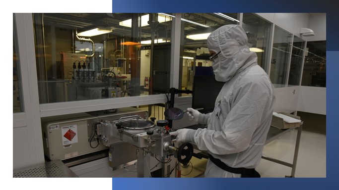
Forge Nano is the global leader in scalable atomic layer deposition (“ALD”), a unique coating technology that produces a protective atomic layer on a range of materials, powders, and products providing greater protection, performance, durability and safety.
Invented in the 1960s, ALD is mainly used in the semiconductor and OLED industries with the technology commonly found in many mobile phone components. Since 2011, Forge Nano has developed a proprietary ALD process that allows for four times faster coating speeds than any other semiconductor ALD tool provider and enables scale for use on powders and larger surface area objects, such as; lithium-ion batteries, hydrogen fuel cells, pharmaceuticals and vaccines, consumer, sporting and apparel products. Forge Nano calls their ALD coating Atomic Armor.
Atomic Armor works especially well for battery materials, where it stabilizes the surfaces at the atomic level. These coatings prevent excessive wear and damage to the batteries by preventing unwanted reactions among the battery’s internal components. Batteries that have Atomic Armor last 100% longer, charge 300% faster, and dissipate heat more effectively.
Over the past decade, Forge Nano has emerged as a market leader in large-scale ALD. In 2021, Forge Nano announced the world’s first ALD enabled battery for space, with the launching of a high energy lithium-ion battery into orbit aboard the SpaceX Transporter-2 rideshare mission. The Li-ion batteries, featuring Forge Nano Particle ALD technology and Enersys Zero Volt Technology were integrated into spire Global, Inc’s LEMUR-2 satellite.
Atomic Armor can improve performance in hydrogen fuel cells, electrolyzers and storage
Since 2019, Forge Nano has collaborated with the U.S Department of Energy’s National Renewable Energy Laboratory, University of Connecticut, Colorado School of Mines and Fraunhofer Institute of Solar Energy Systems in Germany to accelerate the development of more efficient component parts for hydrogen fuel cells, electrolyzers and hydrogen storage technology. In the hydrogen value chain, Forge Nano’s Atomic Armor can transition fuel cells away from low-scale, costly electrode fabrications while increasing durability and limiting the use of platinum group metals. This reduces both the cost of the fuel cell as well as the technology’s dependence on expensive metals.
Mr David Wu, President of Ascent Funds said, “At Ascent, we look for transformational technology that can have an immediate and profound impact on the energy transition, especially in the hydrogen ecosystem. With over a decade’s experience in enhancing lithium-ion batteries and other materials, Forge Nano is the only commercially large-scale ALD player that can offer a real step-change in productivity, performance and cost for hydrogen companies. For example, instead of using expensive platinum or titanium catalysts, fuel cells could use low cost metal catalysts coated with atomic armor. Until now, atomic armor for hydrogen technology was a theoretical ambition because it couldn’t be scaled – today, atomic armor is a reality’.
Mr. Paul Lichty, CEO of Forge Nano, said: “We are excited to have Ascent join us as investors and advisors. They have a strong track record in identifying game changing technologies and helping those companies to scale and commercialize. In addition, Ascent’s knowledge and experience across the global hydrogen industry will be paramount as our technology becomes an accelerant in the energy transition, particularly for mobility, be it BEV or FCEV.”
Ascent joins existing shareholders Volkswagens, LG Chem, Air-Liquide, Mitsui Kinzoku, Sumitomo and SCG from Thailand.


%20(1).png)