Friday, February 5, 2016

Amtech’s & SoLayTec’s solar tool orders boosted in South East Asia

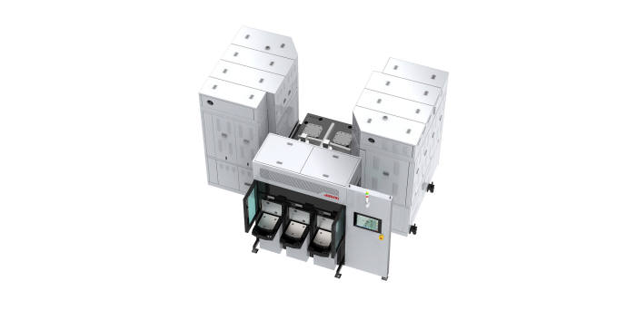
Amtech Systems Inc., who recently bought Dutch Spatial ALD equipment manufacturer SoLayTec reports: TEMPE, Ariz., Feb. 4, 2016 /PRNewswire/ -- Amtech Systems, Inc. (NASDAQ: ASYS), a global supplier of production equipment and related supplies for the solar, semiconductor, and LED markets, today announced its solar segment, consisting of Tempress Systems, Inc., R2D Automation, and SoLayTec, received approximately $12 million in new solar orders in January, including orders for SoLayTec's ALD systems. The orders are expected to ship within the next six to twelve months.

Fokko Pentinga, Chief Executive Officer of Amtech, commented, "We are pleased with the strong level of bookings to start to our fiscal second quarter, and continue to see healthy quotation activity within our solar segment."

  SoLayTec in Eindhoven, Netherlands,  develops, produces and services production systems for ultrafast, spatial Atomic Layer Deposition, a promising technology for ultrathin Al2O3 passivation layers on solar cells. (www.solaytec.com)

The view by Intel on Moore`s Law and Beyond cmos

Here is an interesting article in EE Times on the future of Moore`s law in the view of Intel’s top fab executive, speaking to an audience of chip designers:


 “The economics of Moore’s Law are sound if we focus on reducing cost per transistor,” William Holt told about 3,000 attendees of the International Solid-State Circuits Conference (ISSCC) here. But “beyond CMOS we’ll see changes in everything, probably even in computer architecture,” he said.


Full article: http://www.eetimes.com/document.asp?doc_id=1328835

Thursday, February 4, 2016

CMC² 2016 Call for Papers & Registration, May 5-6, Hillsboro, Oregon USA

 
CMC² 2016 Call for Papers
The Critical Materials Council (CMC) and TECHCET have issued a call for papers to be presented at the CMC Conference to be held May 5-6, 2016 in Hillsboro, Oregon, USA. Semiconductor manufacturing industry experts from IDMs, OEMS, and materials suppliers will gather to discuss actionable information on critical materials used in HVM fabs surrounding the theme of "Critical Materials for Device Driven Scaling", while also looking at issues associated with new materials needed for future devices. Tim G. Hendry, Vice President, Technology & Manufacturing and Group Director of Fab Materials, Intel Corp., will provide the keynote address.
Following the annual members-only Critical Materials Council meeting to be held May 3-4, the 2016 CMC Conference is open to the public. Business drives our world, but technology enables the profitable business of manufacturing new devices in IC fabs, and new devices need new materials. In addition to panel discussions, presentation sessions will focus on the following topics:
I. Semiconductor Market Briefing: application-specific demands for devices and materials
II. Tracking the Supply Chain down to Earth, Wind, and Fire: manufacturing and supply chain 
III. Emerging Materials Evolutions: alternate logic channels and new memory switches, and
IV. Materials Revolutions: beyond silicon CMOS.

To submit a paper for consideration, please send a 1-page abstract focusing on critical materials supply dynamics by March 4, 2016 to cmcinfo@techcet.com.
Click here for a pdf version of this Call for Papers.
Attendees will include industry experts handling supply-chains, business-development, R&D, and product management, as well as academics and analysts. The early-bird registration fee (before April 15th) for the CMC Conference is $349; the standard registration fee is $425 (after April 16th).  CMC member companies will be attending this meeting, as it is an important part of their membership.  
On behalf of the CMC Conference Committee,
Lita Shon-Roy, Jonas Sundqvist, Ph.D., Ed Korczynski
CMC Conference 2016 Registration is Now Open!
Register by April 15 for early bird discount, price of $349!
Dates: May 5-6, 2016*
Location: Hillsboro, Oregon - The Embassy Suites Hotel
Click for the  CMC Conference Page
For up to date agenda details, click here.
*This is the open forum portion of the CMC regularly scheduled meeting.

CMC Support and Sponsorship Opportunities
It is our continued goal to provide up to date, relevant information on the supply markets of critical materials through education and collaboration of industry professionals. None of this is possible without the help of our sponsors!
To learn more about sponsorship opportunities click here to be taken to the CMC Fabs website. 


Wednesday, February 3, 2016

ALD History Blog: VPHA abstract to ALD 2016 Ireland - DL Feb 7

ALD History Blog: VPHA abstract to ALD 2016 Ireland - DL Feb 7: The webpage of ALD 2016 in Dublin, Ireland, July 24-27, http://ald2016.com/ has been updated and abstract submission is open.

From VPHA, there will be one abstract to ALD 2016 (Item #9 in the Publication Plan). The contents of the presentation will be a summary of the historical ALD papers and a recommended reading list, created together by the VPHA group, based on the contents of the ALD-history-evolving-file. All those will be listed as authors of the presentation, who have participated in the voluntary VPHA reading and left at least one comment in the ALD-history-evolving-file by the time of sending the abstract. We have at the moment 41 co-authors from 12 countries (Poland joined recently).

The deadline of ALD 2016 is February 14. The VPHA internal deadline should be somewhat earlier; let us make this one week. If you'd like to join the VPHA abstract as an author, please make your first comment in the ALD-history-evolving-file no later than on February 7, 2016. People can of course join the voluntary VPHA reading later than this, too,only then their name will not appear in the ALD 2016 abstract.

Tuesday, February 2, 2016

EuroCVD-BalticALD 2017 Sweden Update: Invited Speakers & Tutorials

Here are some updates on the the CVD-ALD bonanza that will take place in Linköping, Sweden 2017. We will organize a joint EuroCVD-BalticALD meeting over three packed days 11-14 June,  four days in total as there will be tutorials on Sunday and a welcome mixer in evening.

The event is now also open for sponsoring & exhibition, please contact us for more information.

Hope to see many of you in Linköping Sweden summer 2017!

Kind regards,
Henrik Pedersen, Linköping University, Chair
Jonas Sundqvist, Lund University / Technical University of Dresden
Sean Barry, Carleton University
Mats Boman, Uppsala University


Invited speakers:

Angel Yanguas-Gil
Argonne National Laboratories, USA

Martin Magnusson
Lund university, Sweden

Stacey Bent
Stanford University, USA

Claire Carmalt
University College London, UK

Annelies Delabie
KU Leuven, Belgium 


Sunday tutorials will be held at Linköping University, Campus Valla and be focused on surface chemistry for CVD and ALD

Tutors:

Simon Elliott
Tyndall Institute, Ireland

Francisco Zaera
University of Californa, Riverside, USA

Maarit Karpinnen
Alto University, Finland 

Scienific Committee: 

Henrik Pedersen, Linköping University, Sweden
Jonas Sunqvist, TU Dreseden/Lund University, Germany/Sweden
Sean Barry, Carleton University, Canada
Mats Boman, Uppsala University, Sweden
Ray Adomaitis, University of Maryland, USA
Markku Leskelä, University of Helsinki, Finland
Jaan Aarik, Tartuu University, Estoina
Kaupo Kukli, Tartuu University, Estoina
Martyn Pemble, Tyndall Institute, Ireland
Mato Knez, nanoGune, Spain
Anajan Devi, Ruhr-Bochum University, Germany


UPDATE: Area Selective Deposition Workshop - ASD 2016 hosted by Imec

Imec and the COST action HERALD will host a workshop dedicated to Area Selective Deposition “ASD 2016”, at imec in Leuven, Belgium on April 15th, 2016. This workshop will provide an excellent opportunity for the R&D community to learn about Area Selective Deposition and it will offer a forum for open discussions between researchers from academia and industry. We look forward to your participation.


The workshop will focus on the fundamental mechanisms of ASD processes and nucleation, as well as on the challenges related to the characterization of selectivity. Potential applications of selective deposition will be discussed.


The 1 day program will consist of:
  • Presentations by invited speakers on the fundamentals and characterization of selectivity
  • A panel discussion about potential applications of selective deposition
  • A poster session covering selective deposition as well as nucleation. Poster contributions are welcome by abstract submission
  • Coffee breaks, lunch and diner
Confirmed invited speakers: 
Soley Ozer (Intel), Mikko Ritala (Helsinki University), Erwin Kessels (TU Eindhoven), Simon Elliott (Tyndall National Institute), Gregory Parsons (North Caroline State University), Christos Takoudis (University of Illinois at Chicago), Hyungjun Kim (Yonsei University), Wilfried Vandervorst (imec), Manfred Buck (St Andrews University), Jim Engstrom (Cornell University)
Registration module is open - Deadline: March 25th, 2016.
- Poster contributions are welcome by abstract submission (see website). Deadline: March 15th, 2016. The poster session is covering area-selective deposition as well as nucleation.
- HERALD travel support: HERALD members can apply for travel support by sending a short motivation letter and CV to asd2016@imec.be. Deadline: March 2nd, 2016.


More information is available at http://www2.imec.be/be_en//education/conferences/asd-workshop-2016.html

Monday, February 1, 2016

Metal Amidinates from Strem Chemicals for ALD

As reported earlier here on the BALD Blog - Strem Chemicals & Harvard University has signed a deal on distribution of ALD metal amidante precursors out of the UK. Presumably the deal that Dow left when exiting the booming ALD precursor business.

Here is a link too the new offering: http://www.strem.com/catalog/family/Metal+Amidinates/ 


Epiluvac and SAMCO to offer processing equipment for WBG materials in Nordic countries

As earlier reported here on the BALD Blog Epiluvac from Sweden and SAMCO from Japan has signed a collaboration deal. Now the to partners have signed an extened agreement to include distribution of SAMCO products in Scandinavia. Interestingly SAMCO also have an ALD product line. See also previous report on ALD here.


 Epiluvac’s EPI-1000X silicon carbide reactor.


SAMCO's new AL-1 ALD system.
 
As reported by Solid State Technology : Sweden-based SiC CVD developer and manufacturer Epiluvac AB has entered into a collaboration with SAMCO, a semiconductor process equipment developer and manufacturer based in Japan, in which Epiluvac will introduce new clients to SAMCO in Sweden, Norway, Finland and Denmark.


Bo Hammarlund, Chair , CEO, founder  of Epiluvac AB
 
SAMCO offers systems and services that revolve around three major technologies: 1) thin film deposition with PECVD, MOCVD and ALD systems, 2) microfabrication with ICP etching, RIE and DRIE systems, and 3) surface treatment with plasma cleaning and UV ozone cleaning systems.

“With this collaboration, Epiluvac and SAMCO are both acting as a one-stop solution,” says Bo Hammarlund, managing director of Epiluvac AB. “We offer our expertise to help customers decide upon the best combinations in terms of processing equipment for WBG materials, including both SiC and GaN materials.”

Australian company Audio Pixels employing ALD for new generation of MEMs Digital Speakers

Australian company Audio Pixels reports on using ALD as a key technology for their new MEMs based speakers. An Audio Pixels speaker is a MEMS chip roughly 1 mm thick. The chip replaces conventional speaker driver(s), enclosure or acoustic chamber, as well as the electronic circuitry associated with converting the digital signal feed to analog. The reoprt belwo doens´tell us exactly how ALD is employed but oyu can imagine it beeing used in the 3D pixelated speaker elements.


Press release: The Company is pleased to announce that it has reached the first verification stage, of the fourth and final phase of the commercial product development plan. The company has recently received and began testing the first batch of verification wafers. Verification wafers allow our teams to examine, test and validate characteristics, progress and compliance of the MEMs chips during and throughout the fabrication process in order to better ensure, to the maximum extent possible, successful fabrication of Phase-IV chips. 


ASM International Shares Bought by EQIS Capital Management

As reported numerous times here on the ALD Blog, ALD is booming and especially for semiconductor equipment manufacturers like ASMi with a considerable part of their sales in ALD (HKMG, spacer, liners, multiple patterning). According too Gartner, VLISI and others the forecasted growth for single wafer ALD processing equipment i supposed to double until 2018.

EQIS Capital Management boosted its position in ASM International NV - The world´s leading ALD Company, by 8.7% during the fourth quarter, according to its most recent Form 13F filing with the Securities and Exchange Commission. The firm owned 9,302 shares of the company’s stock after buying an additional 741 shares during the period. EQIS Capital Management’s holdings in ASM International NV were worth $367,000 as of its most recent SEC filing.


Separately, Morgan Stanley assumed coverage on ASM International NV in a research report on Tuesday, December 15th. They set an “overweight” rating for the company. 

Full report by Corvus Business : http://corvuswire.com/2016/01/27/asm-international-nv-asmi-shares-bought-by-eqis-capital-management/779529/

Friday, January 29, 2016

HERALD Novel High-k Workshop Call for abstracts until Jan 31, 2016 - Working Group 4 Event

Reminder: Call for abstracts until Jan 31, 2016 - Working Group 4 Event

In collaboration with the EU COST networking project HERALD, NaMLab invites to the ‘Novel High-k Application Workshop’ on March 14th and 15th, 2016. New challenges offered by the application of high-k dielectric materials in micro– and nanoelectronics will be discussed by more than 80 participants from industry, research institutes and universities. The workshop was initiated as a stimulating European platform for application-oriented scientists to exchange ideas and discuss latest experimental results on MIM-capacitors, process technologies, leakage & reliability as well as characterization of high-k dielectrics integrated in silicon based micro– and nanoelectronics. In addition, new results in the field of ALD dielectrics in solar cells, transparent conduction oxides (TCOs) and atomic layer etching (ALE) will be discussed.

A long list of speakers already confirmed their participation at the workshop. A preliminary program can be found here: http://www.namlab.com/news/events-1/novel-high-k-application-workshop.

To participate in the workshop, please apply by the end of January 2016 with a ½ page abstract (oral or poster) describing the work you would like to present. Mail your abstract to ALD@namlab.com

Since the HERALD project aims to promote participation from new EU member countries, additional travel grants (up to €300 per person) are available. If you would like to apply for a travel grant, please state this in your email.

COST Action MP1402 - HERALD
Hooking together European research in Atomic Layer Deposition


Wednesday, January 27, 2016

IBM Research present InGaAs on insulator FinFET process using Plasma Enhanced ALD HKMG

IBM Research GmbH in Switzerland has developed an n-channel indium gallium arsenide (InGaAs) on insulator fin field-effect transistor (FinFET) process and claims the highest on-current to date for CMOS-compatible InGaAs devices integrated on silicon (Si) [Vladimir Djara et al, IEEE Electron Device Letters, published online 1 January 2016].

According to the paper, the devices were fabricated using a replacement metal gate (RMG) flow, including ultra-thin SiN spacers, scaled high-k/metal gate (HKMG), and highly-doped raised source and drain (RSD) modules for improved electrical performance.

ALD Inside:
  • 12-nm-thick SiN spacers were deposited by plasma-enhanced atomic layer deposition (PEALD)
  • After dummy gate removal, a HKMG, featuring a scaled Al2O3/HfO2 dielectric stack with a capacitance equivalent thickness (CET) of ∼1.5 nm, was deposited using a highly conformal and uniform PEALD process. the process has previously been published here.  The tool used is a FlexAL ALD from Oxford Instruments and the PEALD processes are TMA and O2 plasma for Al2O3 and TEMAH and O2 plasma for HfO2.
The FlexAL® systems provide a new range of flexibility and capability in the engineering of nanoscale structures and devices by offering remote plasma atomic layer deposition (ALD) processes and thermal ALD within a single ALD system.

Pretty cool if you ask me to see that PEALD is used for gate dielectric, which is usually not the case on silicon channels where thermal HfCl4/H2O process is dominating and also that TEMAHf can perform this good as a gate dielectric. Please read the full report in Semiconductor Today here.

Trending ALD News January 2016

Tuesday, January 26, 2016

ALD sales booming for Arradiance GEMStar XT line

It seems that the rather wicked prognosis made by Gartner and others that ALD equipment market will doouble until 2018 may really be for all and not only the semiconductor OEMs. Here is goood news froom Arradiance that are steaming away!


As announced by Arradiance: Sales of GEMStar XT benchtop ALD systems including rapid market adoption of the new GEMStar XT-P plasma-enhanced system resulted in 73% sales growth in 2015 Coupled with a strengthened balance sheet, Arradiance expects to outgrow the market again in 2016.

GEMStar-8 XT PEALD™ Benchtop PEALD/Thermal ALD System


Arradiance LLC, manufacturer of the popular GEMStar family of benchtop Atomic Layer Deposition (ALD) systems for research and light production, today announced an impressive 73% sales growth for 2015 of their highly popular GEMStar family of benchtop Atomic Layer Deposition (ALD) systems for research and light production. 

“We are extremely gratified by the market acceptance of our GEMStar XT line of thermal ALD systems. Most notable is the adoption of our new GEMStar XT-P plasma plus thermal system; the world’s only commercial benchtop, plasma-enhanced tool,” said Arradiance President, Ken Stenton. 

The reactors are stackable!


“Introduction of plasma capability to our benchtop architecture has raised the profile of the product line to a new level,” explained Mr. Stenton. “Customers now view Arradiance as a full-service ALD equipment company, on par with or exceeding the capabilities of companies that offer much larger and more expensive commercial systems. The number of films and applications being developed on the GEMStar systems is growing geometrically.”

Arradiance entered the ALD equipment market in 2010 and has since become one of the fastest growing companies in a crowded field. Customers cite innovation, attention to design detail and superior aftermarket service as some of the reasons for the company’s growing success. Looking forward, Mr. Stenton predicted that, “Coupled with an increased level of support from our investment partners, our existing backlog and sales pipeline should propel Arradiance sales growth to again outpace the market in 2016. Driven by new applications in energy, bio-engineering and high energy physics, demand for reasonably priced, full feature ALD systems continues to grow.”

UPDATE: Jusung Engineering launches SDP R2 Revolution-Rotation ALD System at SEMICON Korea

JUSUNG Engineering Co., Ltd., incorporated founded in 1995, is one of the leading equipment makers in global semiconductor, flat panel display and solar cell markets from South Korea. Today at SEMICON Korea Jusung announced a new cool ALD platform (Press release, Korean) and in English below (supplied by Jusung Engineering).


SDP R2(Revolution/Rotation Atomic Layer Deposition System), featuring entirely new concept chamber to realize high-quality film even at an ultra-low temperature (Picture from Jusung Engineering Korean Press release).


JUSUNG Engineering (Ticker 036930; CEO Chul Joo Hwang) will participate in the SEMICON Korea 2016, an international semiconductor equipment and material expo held in the Coex for three days starting from January 27th 2016 to showcase its next-generation semiconductor equipment.

JUSUNG plans to launch its state-of-the-art products including SDP R2(Revolution/Rotation Atomic Layer Deposition System), featuring entirely new concept chamber to realize high-quality film even at an ultra-low temperature.


 The SDP R2 is new concept equipment that enables revolution for the main disc and rotation for the water simultaneously in order to fulfill the demanding technical requirement in the multi-patterning process at the tech-migration which is at the verification test stage on the mass- production line of a customer.

The equipment allows film quality deposition without using plasma even at an ultra low temperature below 80℃, causing no damage to film quality at infrastructure, and enables the plasma function at the treatment process, realizing the merits of both thermal deposition and plasma deposition processes at the same time. Above all, the most notable feature of the equipment is the ability to control the uniformity of the deposition material in a 20nm or smaller micro semiconductor structure through revolution and rotation function, ensuring excellent film quality without regard to the complexity of the infrastructure.

Once the new concept technology is applied to mass-production, the application will be widely extended to processes such as next-generation memory semiconductor, DRAM and Flash thanks to improved semiconductor film quality profile along with reduced time requirement for deposition, leading to higher productivity as well as lower cost.

An officer from JUSUNG Engineering said, “We showcase new concept equipment that is optimized to the tech migration process at an event where you can see the recent technology trends in the semiconductor industry at a glance…We will do our utmost to keep our technology well ahead in the industry with new product development to overcome limitations of existing equipment for next-generation semiconductors.”

Picosun sees growth for their clustered ALD Batch Product line in the growing MEMS industry


Earlier this year this blog reported on expected growth for ALD OEMs due to capital investments driven by 14 & 10 nm at TSMC and other Foundries - 2016 will be a good year for the ALD Equipment Manaufacturers. Another area that is rapidly introducing ALD processes is MEMS. Finnish ALD Company Picosun is experiencing revenue from the MEMS Industry and sees a big future growth opportunity in this area, having a competitive edge by their batch ALD cluster tools.

In 2014, the MEMS sector represented an $11.1B business for Si-based devices according to Yole Développement (Yole) latest MEMS report “Status of the MEMS Industry”.

According to Yole, the MEMS industry is forecasted to exceed $20B by 2020 and lead by the “MEMS Titan” Robert Bosch (Bosch). Picosun and Bosch  has a collaboration in ALD as announced in 2014 (http://www.picosun.com/sitenews/view/-/nid/117/ngid/4). So it indeed seems that Picosun is very well positioned to take on a lead as a Tier1 ALD MEMS supplier.


Passivation of MEMS by Atomic Layer Deposition, Matthias Schwille, Robert Bosch (ALD Lab Dresden Symposium, SEMICON Europa 2015)

Under this new analysis entitled, “Status of the MEMS Industry” report Yole proposes a deep understanding of the MEMS markets trends and players dynamics. The More than Moore market research and strategy consulting company announces its 2014 MEMS manufacturers and foundries ranking and proposes an overview of the future game-changers including new devices, disruptive technologies, 300mm wafers, sensor fusion and new markets.


As reported by Picosun: Picosun Oy, the leading supplier of high quality ALD (Atomic Layer Deposition) thin film coating solutions for industrial production, has revolutionized cost-effective MEMS manufacturing with high throughput PICOPLATFORM™ batch ALD cluster technology.


MEMS (MicroElectroMechanical Systems; Microsystems) are micrometer-scale, semiconductor-based components that combine e.g. electrical, mechanical, and optical functions. They are present in our everyday electronics in products such as hard disk read heads, inkjet printer nozzles, microphone and videoprojector chips, and airbag controls, tire pressure monitoring, and driving stability systems in cars.

Fast, fully automated and economically feasible batch processing without compromising the strictest process quality and purity requirements of the semiconductor industries is the prerequisite for industrial breakthrough of the next generation MEMS devices. They realize improved data storage, mobile phone, GPS positioning, and automotive control electronics, and health care applications such as body area sensors and remote monitoring devices. Combining batch ALD processing with fully automatic, robotized PICOPLATFORM™ vacuum cluster systems enables super-fast throughput of MEMS chips with excellent yield, process purity and uniformity levels(*). 


Team Picosun

“Our MEMS customers gain immense benefits from our SEMI S2 certified PICOPLATFORM™ cluster technology. Equipped with our production-proven PICOSUN™ P-series batch ALD tools, these cluster systems have already proven their worth at the manufacturing sites of leading, global microsystems industries. Considering the MEMS market growth forecasts, propelled by the coming era of the Internet-of-Things, this product line will definitely be one of the cornerstones of our industrial ALD business,” states Mr. Timo Malinen, Chief Operating Officer of Picosun.

(*) Within-wafer, wafer-to-wafer, and batch-to-batch film thickness non-uniformity values (1σ) measured with 50 nm Al2O3 process on 200 mm Si wafers (25 wafers/batch) < 1%. The development work for batch ALD cluster technology has been performed in the project Lab4MEMS (1.1.2013 - 31.12.2015), coordinated by ST Microelectronics.

The project Lab4MEMS has received funding from the EC under the ENIAC Nanoelectronics Framework Programme (ENIAC-2012-2) under grant agreement no 325622-2.


Sunday, January 24, 2016

Strem Chemicals & Gordon Lab at Harvard collaborating on ALD Precursors


According to a recent press release (below) Strem Chemicals inc. in the US is now collaborating with the famous Gordon Research Group at Harvard on transition metal amidinate ALD Precursors. This collaboration includes the distribution of those precursors out of The UK and Ireland. Earlier the distribution here in Europe was through DOW but as previously reported DOW has dropped ALD precursors - so this is very good news for us here in Europe that Strem who has excellent distribution services will handle of this business here. Luckily I just got the new catalog from Strem and could look up some of these precursors including in the deal between Strem and Harvard (see pictures below).


Families of volatile metal available for use in ALD applications

Strem Chemicals Inc in the US works with Roy Gordon’s Group at Harvard University, who produce transition metal amidinates for metal, nitride and oxide layer deposition, allowing Strem Chemicals UK to distribute them in the UK and Eire.
Atomic Layer Deposition (ALD) is a vapour phase technique capable of producing thin films of a variety of materials.  As device requirements push toward smaller and more spatially demanding structures, ALD has demonstrated potential advantages over alternative deposition methods.  ALD offers exceptional conformity on high-aspect ratio structures, thickness control at the angstrom level, and tunable film composition from metal oxides to noble metals.  ALD has emerged as a powerful tool for many industrial and research applications including ferroelectric memories, switches, radiation detectors, thin-film capacitors and microelectromechanical structures (MEMS).  They also are affording significant improvements in solar cell devices, high-k transistors, solid oxide fuels, protective coatings, fuel cells, + ion- batteries and nanogratings. 

Saturday, January 23, 2016

Lam Research is taking a lead in Atomic Layer Etching (ALE)

Lam Research is taking a lead in Atomic Layer Etching (ALE) and is moving on fast introducing leading etch processing equipment for the advanced nodes.


 Lam Research reports in a recent article in Semiconductor Engineering (here): 

Atomic layer etching (ALE) is a technique for removing thin layers of material using sequential reaction steps that are self-limiting. ALE has been studied in the laboratory for more than 25 years. Today, it is being driven by the semiconductor industry as an alternative to continuous etching and is viewed as an essential counterpart to atomic layer deposition. As we enter the era of atomic-scale dimensions, there is need to unify the ALE field through increased effectiveness of collaboration between academia and industry, and to help enable the transition from lab to fab. With this in mind, this article provides defining criteria for ALE, along with clarification of some of the terminology and assumptions of this field. To increase understanding of the process, the mechanistic understanding is described for the silicon ALE case study, including the advantages of plasma-assisted processing. 


ALE Review by Keren Kanarik et al "Overview of atomic layer etching in the semiconductor industry" J. Vac. Sci. Technol. A 33, 020802 (2015); http://dx.doi.org/10.1116/1.4913379

A historical overview spanning more than 25 years is provided for silicon, as well as ALE studies on oxides, III–V compounds, and other materials. Together, these processes encompass a variety of implementations, all following the same ALE principles. While the focus is on directional etching, isotropic ALE is also included. As part of this review, the authors also address the role of power pulsing as a predecessor to ALE and examine the outlook of ALE in the manufacturing of advanced semiconductor devices.

For those of you that have missed the fantastic animation by Lam explaining ALE - here it comes again.

 
To learn more about ALE you should consider going to Dublin this summer for the ALD 2016 Conference which is also hosing the AVS ALE 2016 Workshop!


Hurry up ALD & ALE People - These articles on Atomic Layer Processing have been made free to download for a limited time!

Hurry up ALD & ALE People - These articles on Atomic Layer Processing have been made free to download for a limited time!


Journal of Vacuum Science & Technology A - 
First 2016 Issue Online Special Issue on ALD/ALE
2.322 
Impact Factor


Gartner says that 7nm will be delayed and 5nm will be pushed out ot 2023

10 nm FinFET may start to ship as early as end of 2016. However, according to a recent article by Mark Lapedus (at Semiconductor Engineering) Bob Johnson, an analyst at Gartner, projects that 7nm could get pushed out to 2020. "This, in turn, could impact the potential timing of 5nm, if the industry decides to move forward with the technology. “I assume 5nm will happen, but not by 2020,” Johnson said, adding that a viable 5nm process may not appear until the next decade, possibly 2023."

The slow down in scaling is not something new and has been seen for some time now. Above is a forecast presented at 2014 Semicon West with conclusions of the SEMI’s World Fab Forecast - Technology Node Transitions Slowing Below 32 nm. Her you can clearly see that the node transitions has paced slower since 28/32 nm.  The question now is then if the pace will come to a halt.

The current 3 main options for 5nm logic FETs are :
  • Gate-All-Around FETs based on III/V Nanowires
  • To extend FinFET
  • Monolithic 3D and other 2.5D/3D IC technologies

AVS ALE 2016 - Call for Papers, Dublin, July 24-25th

ALE 2016 - Call for Papers!

In conjunction with ALD 2016 in Dublin, Ireland, the AVS Plasma Science and Technology and Thin Film Divisions will be hosting the 3rd workshop on Atomic Layer Etching. 

Deadline: March 18, 2016 : http://ald2016.com/atomic-layer-etching-workshop-overview/


Plenary Speaker

•Ankur Agarwal (Applied Materials)

Invited Speakers
• Steven George, University of Colorado, Boulder
• Dennis van Dorp, IMEC
• Akira Koshiishi, Tokyo Electron
• Kazunori Shinoda, Hitachi Hi-Tech

ALE 2016 Workshop Overview

Extending Moore's law beyond the 10 nm node will increasingly rely on high precision processes employing new materials with high-quality surfaces. Atomic layer etching & atomic layer clean technology is a promising pathway to achieve these fundamental requirements.

In conjunction with ALD 2016 in Dublin, Ireland, the AVS Plasma Science and Technology and Thin Film Divisions will be hosting the 3rd workshop on Atomic Layer Etching. The 2nd ALE workshop was held in 2015, and attracted global participation, with nearly 280 attendees representing both academia and industry. The goals of the meeting are to provide research focus, report progress to-date, and foster collaboration to accelerate this unique capability. Latest findings are expected from experts at major universities, semiconductor manufacturers, and leading equipment suppliers. A broad range of topics are expected, including but not limited to:

• Surface chemical reactions
• Ion energy distributions and control
• Damage-free processes
• Modeling of processes and discharges
• Chemistry synthesis for 'reverse ALD'
• Interesting and new applications for ALE

Workshop Chairs

Bert Ellingboe, Dublin City University (albert.ellingboe@dcu.ie)

Sumit Agarwal, Colorado School of Mines (sagarwal@mines.edu) 


Friday, January 22, 2016

2016 Critical Materials Council (CMC) Seminar – Call for Papers

The Critical Materials Council (CMC) and TECHCET have issued a call for papers to be presented at the “Critical Materials for Device Driven Scaling” Seminar to be held May 5-6, 2016 in Hillsboro, Oregon, USA. Semiconductor manufacturing industry experts from IDMs, OEMS, and materials suppliers will gather to discuss actionable information on critical materials used in HVM fabs, while also looking at issues associated with new materials needed for future devices. Tim G. Hendry, Vice President, Technology & Manufacturing and Group Director of Fab Materials, Intel Corp., will provide the keynote address.


Following the annual members-only CMC meeting to be held May 3-4, the 2016 CMC Seminar is open to the public. Business drives our world, but technology enables the profitable business of manufacturing new devices in IC fabs, and new devices need new materials. In addition to panel discussions, presentation sessions will focus on the following topics:

I. Semiconductor Market Briefing: application-specific demands for devices and materials
II. Tracking the Supply Chain down to Earth, Wind, and Fire: manufacturing and supply chain
III. Emerging Materials Evolutions: alternate logic channels and new memory switches, and
IV. Materials Revolutions: beyond silicon CMOS.

Attendees will include industry experts handling supply-chains, business-development, R&D, and product management, as well as academics and analysts. The early-bird registration fee (before March 15th) for the CMC Seminar is $349; the standard registration fee is $425 (after March 15th). CMC member companies will be attending this meeting, as it is an important part of their membership. Additional information can be found online at http://cmcfabs.org/seminars.

To submit a paper for consideration, please send a 1-page abstract focusing on critical materials supply dynamics by February 29, 2016 to cmcinfo@techcet.com.

The Critical Materials Council for Semiconductor Device Fabricators was originally started by SEMATECH in the early 1990’s, and is now managed by TECHCET. It actively works to identify issues surrounding the supply, availability, accessibility, or lack thereof, of semiconductor process materials, current and emerging, also known as “Critical Materials”. This is done by collectively working to solve common materials related issues in a non-competitive environment. The CMC supports the continuous improvement of the Materials Supply Chain Community for Semiconductor Fabricators. For more information see www.CMCFabs.org .