Saturday, March 6, 2021

Thermal ALE of germanium rich SiGe by CU Boulder and ASM Microchemistry

Epitaxially grown SiGe is an important material for CMOS Logic. It is integrated as the channel material and by inserting a higher concentration of germanium the mobility of the transistor can be improved. The industry calls it Epi, but what is really referred to a thermal CVD process producing an epitaxially grown layer of silicon or silicon-germanium onto a single crystalline silicon wafer.

As CMOS scaling has progressed the IDMs and Foundries have moved from the planar field-effect transistor (FET) architecture to a narrow fin-based transition the FinFET. The next evolutionary step on the horizon will be the transition to a nanowire-based architecture forming a gate-all-around FET (GAA-FET). At some point in time beyond the 2 nm node, the lateral scaling possibility will hit a wall and it is foreseen that the CMOS scaling will gup upwards like other technologies in order to cram in more devices per unit area. In a first approach, it may be that the NMOS and PMOS transistors are rearranged from being processed next to each other to put one of them on top of the other. Intel recently presented this at IEDM2020 (LINK). Having done that you can foresee continuing on a vertical scaling path also for CMOS just like 3DNAND and start to build those skyscrapers.

When going vertical, you will need highly conformal deposition processes as provided by ALD and in high volume production since the event of 90 nm DRAM (Samsung) and 45 nm Logic (Intel), however, etch is a problem since the reactive ion etching process are typically directional with the plasma under low-pressure processing conditions used. Also, the Argon plasma ALE processes to etch Silicon, silicon Germanin gallium nitride, and III/V materials are directional or anisotropic as the etch guys say or non-conformal as we ALD people say.

Typically the best way to achieve isotropic etch conditions, meaning you remove material at the same rate or as for ALE the same amount per cycle (etch per cycle EPC), is to skip the plasma that causes the anisotropic etch. Here Dr Abdulgatov and co-workers in the famous SM George Lab, CU Boulder together with Varun Sharma and friends from ASM Microchemistry, one of Dresden's best shining ALD-Stars, publish a paper on Thermal ALE of germanium rich SiGe that is quite clever. Here using PVD Si0.15Ge0.85 samples, which are difficult to make by Epi due to the high Ge content. I think we will see more of this for also GaN, SiC and III/V materials coming up.


AI Abdulagatov, V Sharma, JA Murdzek, AS Cavanagh, SM George
Journal of Vacuum Science & Technology A: Vacuum, Surfaces, and Films

Abstract: The thermal atomic layer etching (ALE) of germanium-rich SiGe was demonstrated using an oxidation and “conversion-etch” mechanism with oxygen (O2) or ozone (O3), hydrofluoric acid (HF), and trimethylaluminum [TMA, Al(CH3)3] as the reactants. The crystalline germanium-rich SiGe film was prepared using physical vapor deposition and had a composition of Si0.15Ge0.85. In situ spectroscopic ellipsometry was employed to monitor the thickness of both the SiGe film and the surface oxide layer on the SiGe film during thermal ALE. Using a reactant sequence of O2-HF-TMA, the etch rate of the SiGe film increased progressively with temperatures from 225 to 290 °C. At 290 °C, the SiGe film thickness decreased linearly at a rate of 0.57 Å/cycle with a surface oxide thickness of 18–19 Å. This etch rate was obtained using reactant pressures of 25, 0.2, and 0.4 Torr and doses of 1.5, 1.0, and 1.0 s for O2, HF, and TMA, respectively. The TMA and HF reactions were self-limiting and the O2 reaction was reasonably self-limiting at 290 °C. Using an O3-HF-TMA reaction sequence, the SiGe ALE etch rate was 0.42 Å/cycle at 290 °C. This etch rate was obtained using reactant pressures of 15, 0.2, and 0.4 Torr and dose times of 0.5, 1.0, and 1.0 s for O3, HF, and TMA, respectively. The O3, TMA, and HF reactions were all self-limiting at 290 °C. Atomic force microscopy images revealed that thermal ALE with the O2-HF-TMA or O3-HF-TMA reaction sequences did not roughen the surface of the SiGe film. The SiGe film was etched selectively compared with Si or Si3N4 at 290 °C using an O2-HF-TMA reaction sequence. The etch rate for the SiGe film was >10 times faster than Si(100) or Si3N4 that was prepared using low-pressure chemical vapor deposition. This selectivity for the SiGe film will be useful to fabricate Si nanowires and nanosheets using SiGe as the sacrificial layer.

Full text open source: LINK


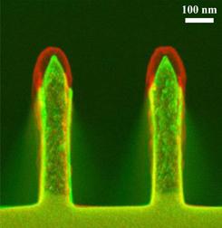
Figure from Journal of Vacuum Science & Technology A 39, 022602 (2021); https://doi.org/10.1116/6.0000834

Friday, March 5, 2021

EMD Performance Materials announces further investments of electronics business and new name: EMD Electronics

  • New name reflects the product and service portfolio designed to enable the future of electronics in a data-driven world
  • Investment into R&D and innovation centers in Tempe and Silicon Valley
EMD Performance Materials today announced an expanded focus on the US electronics business and a new name in the US: EMD Electronics. EMD Electronics, a business of Merck KGaA, Darmstadt, Germany, includes a broad portfolio of semiconductor materials, semiconductor delivery systems and services, display, and surface solutions. The Electronics business globally employs more than 7,400 – with a third of employees in the US across 29 sites, with plans for continued growth in planarization and thin films organizations following recent investments. More information about the Electronics business can be found here.


Additionally, the company announced the relocation of the Silicon Valley Innovation Hub from Menlo Park to Intermolecular's San Jose facilities, combining Merck KGaA, Darmstadt, Germany's innovation efforts in the Bay area with Intermolecular's services for materials and electronics, creating a unique space that empowers collaboration with startups. This announcement follows the $22 million investment at the EMD Electronics site in Tempe, Arizona for its R&D and production for semiconductor materials announced in February.


"Our name change and investment in these centers demonstrate our commitment to continued innovation in electronics and supporting US customers' requirements for capitalizing on growing opportunities driven by digital transformations and data-driven electronics," said Jeff White, President of EMD Electronics. "Our customers are working on cutting-edge technologies and products that range from better immersive displays and surfaces in cars and consumer electronics to how to move neuromorphic and quantum computing to the next level. Our combined expertise and portfolio in display and surface innovations, semiconductor materials and the safe delivery and storage of speciality chemicals and gases will enable new discoveries and novel products not even imagined yet."

As the company behind the companies advancing digital living, the Electronics business sector is involved in all major technology trends – be it 5G, Big Data, autonomous driving, artificial intelligence, or the Internet of Things. Thanks to these and other megatrends, the demand for ever smaller, faster and more energy-efficient electronics is continuously growing. Sample innovations enabled by EMD 

Electronics include:
  • Patterning, deposition and spin-on dielectrics materials to make 3D NAND possible
  • DSA – revolutionary way of building microchips of the future
  • OLED for brighter, thinner, free-form displays
  • Liquid crystals for electronic steerable antennas to bring connectivity to places currently not reachable
  • eyerise ® liquid crystal for greener windows and innovative building architecture
These technologies and innovations are being implemented across a diverse set of customers including larger companies and start-up companies. To enable new inventions for start-ups, EMD Electronics has launched a program for early-stage and growth companies looking to advance their technologies in the areas of displays, semiconductor materials, neuromorphic computing, AI enabled materials development and smart manufacturing by applying for the EvoNexus MarketLink Program by March 12.

Monday, March 1, 2021

Welcome to the RASIRC ALD Oxide Wizard

Welcome to the RASIRC ALD Oxide Wizard. The wizard compares the reactivity of water and hydrogen peroxide for 285 different precursors.
  • Direct theoretical comparison between water and hydrogen peroxide
  • Allows for rapid screening of possible precursors
  • Allows for lower cost precursors to be used where previous water reactivity was too low
  • Allows for visualization of precursors to better understand steric hindrance effects
Starting with the five of the most common metals used in Atomic Layer Deposition (ALD) and 57 common ligands, the wizard creates the desired precursor, visualizes the precursor molecule, and concludes with a determination of reaction energetics (favorable/less favorable) in terms of intrinsic energy changes ∆E added or released in the creation of the metal oxide with H2O2 or water. The wizard allows you to make modifications to the ligand and see the effects on reactivity. Edit your design as many times as you want; when you have your desired reaction, choose the print option.

Enter The RASIRC ALD Oxide Wizard HERE!


Example using the HfI4 H2O vs H2O2 going from -30.3 to -180.5 kJ/mol - The more negative the value, the more thermodynamically likely the reaction is to occur.


Sunday, February 28, 2021

WEBINAR - Longer-lasting implants with hermetic ALD coatings by Picosun

Register for free for Picosun Group 's webinar "Longer-lasting implants with hermetic ALD coatings" where we present our latest results and ALD solutions for medical implant manufacturers. 27 April at 3PM London/10AM New York time.

Registration and information: LINK

Improved reliability and functionality for electronic and orthopedic implants with Picosun’s ALD solutions

With the boom of digital and remote healthcare and the increasing life expectancy of people, there is a rapidly growing need for more and more advanced medical devices, both implanted and external. At the same time, recent advances in microelectronics and the constantly miniaturizing size of the components enable the design of highly sophisticated implanted devices that can be placed in the most sensitive areas of the body such as the brain, spine, heart, and eyes.

Picosun’s Atomic Layer Deposition (ALD) thin film coating technology offers a disruptive solution for implant manufacturers. Hermetic ALD encapsulation improves the reliability, functionality, and lifetime of electronic and orthopedic implants, potentially reducing the need for corrective or replacement surgeries. Also, cost savings can be achieved when the base materials of the implant can be e.g. stainless steels instead of noble or specialty metals.


Norwegian Morrow Batteries and Dutch startup Delft IMP have signed a JDA for ALD improved batteries

Morrow Batteries explores new technology with Dutch startup-company Morrow Batteries and Delft IMP have agreed to explore a joint collaboration in using ultra-thin coating technologies to produce lower cost and more sustainable batteries. Norway-based Morrow Batteries and Dutch-based startup Delft IMP have agreed to investigate the joint development of new improved batteries. The technology used is based on atomic layer deposition (ALD).


“We are applying ultra thin coatings on powder material and can produce these at scale with a unique technology originating from Delft University of Technology.” said Dr. Roderik Colen, CEO of Delft IMP. “It is a matter of time before breakthrough developments using ultra thin coatings become commercially available. The development of Morrow Industrialization Centre (MIC) provides us with a unique opportunity to demonstrate this at scale.”

Press release: LINK

Morrow Batteries AS: LINK

Morrow Industrialization Centre (MIC) will include a pilot manufacturing line and a R&D centre. We aim to start building MIC in 2022 and be operational in 2023.

Morrow Giga Factory will be a giga-scale battery cell manufacturing factory. We are currently evaluating alternative locations and expect to take a decision by the end of 2020. We aim to start cell manufacturing in our giga-scale battery cell factory by the end of 2024.

Delft IMP: LINK

Saturday, February 27, 2021

2021 ISSCC - Plenary Session with Dr. Mark Liu, TSMC Chairman

TSMC recently delivered a plenary session at ISSCC 2021. by Dr. Mark Liu, TSMC Chairman. He gave a vision and path of how semiconductor technologies will continue to innovate over the coming years and decades. Below you can watch the Dr. Liu’s plenary session.

Abstract: The foundry business model, pioneered by TSMC more than three decades ago, brought a sea change to technology innovation and how integrated circuits (ICs) and systems are designed and manufactured. Access to semiconductor technology is no longer limited to large corporations that invest billions of dollars to build a fabrication plant. The foundry model has democratized IC innovation, making it available to all visionaries and innovators.

Today, an open innovation platform that connects innovators with semiconductor-technology providers is a vital link in the global supply chain. Our industry has already begun to look beyond just engineering individual chips manufactured on wafers, and have moved to integrate individual chips into systems. System performance and energy efficiency will continue to advance at historical rates, driven by innovations from many aspects, including materials, device and integration technology, circuit design, architecture, and systems. User applications drives design choices, and design choices are enabled by technology advancements. Advances in an open innovation ecosystem will further lower the entry barriers and unleash the future of innovation.


Friday, February 26, 2021

ASM International N.V. reports its 4Q/2020 operating results and the fourth consecutive year of double-digit growth

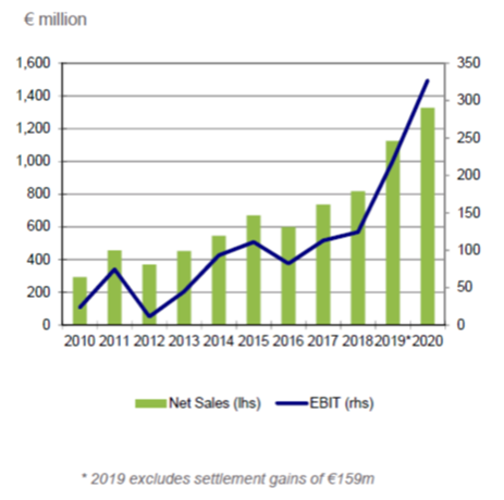
ASM International the leading supplier of single wafer ALD wafer processing equipment in the semiconductor industry reports that 2020 was the fourth consecutive year of double-digit growth.

  • 4Q/2020 was driven by the logic/foundry segment, solid growth in China and a strong increase in spares & service business.
  • ASM expects the single wafer ALD market to reach a size of approx. US$1.5 billion by ‘20-’21, and to grow substantially above that level in subsequent later years. 
  • Next ASM focus is on expanding their addressable market within the single wafer ALD space.

Source: 4Q/2020 Earings press release and investor presentation (LINK)


Area-selective MLD of nylon 6: Growth on carbon and inhibition on silica for a-carbon hardmask repair

Here one of the Editor pic out of the JVSTA Special Topic Collection on Area Selective Deposition. Marcel Junige, is one of Dresden´s top-notch ALD and MLD scientists that went over there to the University of Colorado Boulder to S M Geroge´s famous lab. In this demonstration, it is illustrated the capability of area-selective MLD to repair RIE-eroded aC hard masks and to maintain the critical dimension, which is key in all leading etch semiconductor manufacturing processing schemes. It is a fairly typical situation in this business, the CMP or Etch guys brutally destroy stuff that has to be repaired by ALD or Wet processing, sometimes even by E-Beam single exposure repair. That is maybe one of the drivers behind the more precise and gentle ALE method. Yeah E-CMP ever made it.

Area-selective molecular layer deposition of nylon 6,2 polyamide: Growth on carbon and inhibition on silica

Journal of Vacuum Science & Technology A 39, 023204 (2021); https://doi.org/10.1116/6.0000769
Marcel Junige and Steven M. George


In microelectronic or nanoelectronic manufacturing, pattern transfer by directional reactive ion etching (RIE) progressively erodes amorphous carbon (aC) hard masks. To maintain critical dimensions and tolerances of high-aspect-ratio device structures, new carbonaceous materials may be added repeatedly to replace the eroded aC hard mask. Such a mask repairing step during RIE needs self-aligning growth of organic materials. Area selectivity is required to deposit the organic material on the aC hard mask exclusively. Deposition on the dielectric or semiconductor device structures underlying the mask would complicate their precise etching or later cleaning. When ashing the aC hard mask, all-organic materials are preferable to organic-inorganic hybrid materials because they leave no residue. In this work, area-selective molecular layer deposition (MLD) was developed for the all-organic polyamide nylon 6,2. The monomer reactants for nylon 6,2 MLD were ethylene diamine and adipoyl chloride. Nylon 6,2 MLD was studied in the homogeneous, steady-state growth regime and during nucleation on various starting surfaces utilizing in situ spectroscopic ellipsometry. Area-selective MLD of nylon 6,2 was achieved on the “growth” carbon surface in the presence of silica by functionalizing aC via mild oxidation. In addition, a surface passivant was selectively attached to silica by using an amine-catalyzed coupling chemistry. The passivant inhibited the nylon 6,2 MLD on the “nongrowth” silica surface. A single passivation pretreatment was sufficient to restrict the MLD on the silica surface. The passivant, however, did not substantially impact the MLD nucleation and growth on the aC surface. This strategy yielded area selectivity with exceptionally high quality and over a wide range of MLD cycles. The area-selective MLD of nylon 6,2 was further applied on industrial test features with aC patterns masking trenches in silica. This demonstration illustrated the capability of area-selective MLD to repair RIE-eroded aC hard masks and to maintain the critical dimension.


Tech Insights Teardown: Samsung’s D1z DRAM with EUV Lithography

Advanced and costly schemes for ArFi immersion-based multi-pattering are definitely running out of steam for leading-edge logic and EUV is continuing the march into high volume manufacturing now also for DRAM. The other day there was an announcement that SK Hynix, the world´s number two DRAM maker has signed a 5-year agreement with ASML for EUV scanners (LINK).

As a European, I must say that I like the situation that the key to continued scaling is kept in The Netherlands (ASML) and also the important key technology providers in Germany (Zeiss SMT, Trumpf) and Belgium in the form of the worlds leading research institute for scaling CMOS - imec and the EUV Resist Manufacturing & Qualification Center NV (EUV RMQC), a Joint Venture between imec and  JSR Micro NV (LINK).

Reuters: SK Hynix signs five-year deal worth $4.3 billion with ASML to secure EUV scanners


Now DRAMs from Samsung Electronics with applied EUV lithography technology for D1z DRAM in mass production have been found in the field and analyzed by Tech Insights and reported by EETimes (LINK).

According to EETimes, Samsung Electronics announced the world’s first development of both ArF-i based D1z DRAM and separately its EUV lithography (EUVL) applied D1z DRAM last year.

Tech Insights is excited that we have finally found Samsung’s new and advanced D1z DRAM devices and confirmed details of this technology.

Here just a teaser, please check out the original EETimes article or get the full report from Tech Insights (LINK).


Samsung DRAM cell design, a comparison of BLP patterns on D1z (a) without EUVL and (b) with EUVL.


Wednesday, February 24, 2021

The Nanotechnology Show October 13 - 14, 2021 Edison, New Jersey, USA

The Nanotechnology Show is the first industry-focused exhibition and conference covering the development and integration of nanotechnology within a range of applications including chemicals, life sciences, pharmaceutical, energy, electronics, automotive, and aerospace.

The Nanotechnology Show October 13 - 14, 2021 Edison, New Jersey, USA


The exhibition will provide a comprehensive showcase of the entire supply chain from instrumentation and processing equipment right through to material manufacturers and product developers.


Tuesday, February 23, 2021

Progress and future prospects of negative capacitance electronics: A materials perspective

NaMLab and TU Dresden, who has performed groundbreaking research on Ferroelectric hafnium oxide are also deep into Negtavie Capacitance devices for electronics to come. They have postulated 5 requirements for prospective ferroelectric materials that NC transistors need to fulfill to be useful for practical devices:

1. Robust ferroelectricity at 5 nm thickness and below
2. Compatibility with CMOS technology
3. Thermal stability on silicon
4. Conformal deposition on 3D substrates
5. Large electronic bandgap and conduction band offset to Si

Looking at the number 4 - ALD will come in handy. Enjoy the reading of their prospect paper below, which is open access.

Progress and future prospects of negative capacitance electronics: A materials perspective

Michael Hoffmann, Stefan Slesazeck, and Thomas Mikolajick

APL Materials 9, 020902 (2021); https://doi.org/10.1063/5.0032954

Negative capacitance in ferroelectric materials has been suggested as a solution to reduce the power dissipation of electronics beyond fundamental limits. The discovery of ferroelectricity and negative capacitance in the widely used class of HfO2-based materials has since sparked large research efforts to utilize these effects in ultra-low power transistors. While significant progress has been made in the basic understanding of ferroelectric negative capacitance in recent years, the development of practical devices has seen limited success so far. Here, we present a unique view of the field of negative capacitance electronics from the ferroelectric materials perspective. Starting from the basic principles of ferroelectric negative capacitance, we discuss the desirable characteristics of a negative capacitance material, concluding that HfO2-based ferroelectrics are currently most promising for applications in electronics. However, we emphasize that material non-idealities can complicate and in some cases even inhibit the design and fabrication of practical negative capacitance devices using HfO2-based ferroelectrics. Finally, we review the recent progress on experimental devices and give an outlook on the future direction of the field. In particular, further investigations of the microscopic structure of HfO2-based ferroelectrics are needed to provide an insight into the origin of negative capacitance in this material system and to enable predictive device design


Historic trend of the supply voltage Vdd and equivalent oxide thickness (EOT) scaling in commercial metal–oxide–semiconductor field-effect transistor (MOSFET) technologies. The black dashed line indicates the EOT limit given by the necessary SiO2 interface between the Si channel and the high-k material, and the red dashed lines indicates the minimum supply voltage due to the Boltzmann limit. HKMG: high-k metal gate. NC: negative capacitance.

Thermal Atomic Layer Deposition of Gold: Mechanistic Insights, Nucleation, and Epitaxy

Here is a new paper with deep insights into thermal ALD of gold from Argonne National Lab in the USA. They are using the previously developed precursor from Mikko Titalas ALD group at Helsinki University Finland Me2Au(S2CNEt2). All depositions were carried out in a Veeco CNT Savannah reactor.

Thermal Atomic Layer Deposition of Gold: Mechanistic Insights, Nucleation, and Epitaxy

Pengfei Liu, Yuchen Zhang, Cong Liu, Jonathan D. Emery, Anusheela Das, Michael J. Bedzyk,
Adam S. Hock*, and Alex B. F. Martinson*
ACS Appl. Mater. Interfaces 2021, XXXX, XXX, XXX-XXX
Publication Date:February 9, 2021https://doi.org/10.1021/acsami.0c17943

An in situ microbalance and infrared spectroscopic study of alternating exposures to Me2Au(S2CNEt2) and ozone illuminates the organometallic chemistry that allows for the thermal atomic layer deposition (ALD) of gold. In situ quartz crystal microbalance (QCM) studies resolve the nucleation delay and island growth of Au on a freshly prepared aluminum oxide surface with single cycle resolution, revealing inhibition for 40 cycles prior to slow nucleation and film coalescence that extends over 300 cycles. In situ infrared spectroscopy informed by first-principles computation provides insight into the surface chemistry of the self-limiting half-reactions, which are consistent with an oxidized Au surface mechanism. X-ray diffraction of ALD-grown gold on silicon, silica, sapphire, and mica reveals consistent out-of-plane oriented crystalline film growth as well as epitaxially directed in-plane orientation on closely lattice-matched mica at a relatively low growth temperature of 180 °C. A more complete understanding of ALD gold nucleation, surface chemistry, and epitaxy will inform the next generation of low-temperature, nanoscale, textured depositions that are applicable to high surface area supports.


Thursday, February 18, 2021

Ferroelectric Field Effect Transistors (FeFETs) Bring Promise And Challenges

It is truly amazing to see the progress of FMC in Dresden and the recent drive in the semiconductor industry for Ferro FETs. Continuously you read about involvement from many of the big names in the industry. Here is a very good overview of the current status written by Bryon Moyer at Semiengineering.

[Article in Semiengineering]: Ferroelectric FETs (FeFETs) and memory (FeRAM) are generating high levels of interest in the research community. Based on a physical mechanism that hasn’t yet been commercially exploited, they join the other interesting new physics ideas that are in various stages of commercialization.

“FeRAM is very promising, but it’s like all promising memory technologies — it takes a while to get beyond promising,” said Rob Aitken, fellow and director of technology on the research team at Arm. “It has the potential to have better benefits than the other new non-volatile memory (NVM) technologies that are on the table today.”

Ferroelectric behaviors are opening up opportunities for non-volatile memory, combined logic/memory functions, and neuromorphic modeling. While it’s still early days for the technology, developers are cautiously optimistic about its future.

Source/Full version: LINK

CEO interview: FMC’s Pourkeramati on roadmaps, turning away investors
https://www.eenewsanalog.com/news/ceo-interview-fmcs-pourkeramati-roadmaps-turning-away-investors


The annealing and zirconium quantity have a strong impact on the crystal arrangement. Source: FMC


Friday, February 12, 2021

SIA Webinar: A Review of the 2020 Semiconductor Market and a Look to 2021

2020 proved to be one of the more unique years in recent times in terms of semiconductor market performance. Pre-2020 market forecasts were quickly and fundamentally rethought at the start of the year, as the COVID-19 pandemic upended the world. Significant uncertainly on how semiconductor sales would react to the pandemic existed for much of the year, especially during the first half. As monthly World Semiconductor Trade Statistics sales figures rolled in through the latter half of 2020, it became clear 2020 sales would end up better than most had initially feared.

Please join a panel of semiconductor market experts to help us make sense of the trends that shaped the semiconductor market in 2020 and look ahead to what the market has in store for 2021. Panelists include: Andrea Lati, Vice President, Market Research at VLSI Research; Dale Ford, Chief Analyst at the Electronic Components Industry Association (ECIA); and C.J. Muse, Senior Managing Director, Head of Global Semiconductor Research at Evercore ISI. The session will be moderated by Falan Yinug, Director of Industry Statistics and Economy Policy at SIA.
Presentations:

Andrea Lati, VLSI Research


Safer medical devices with Picosun’s antimicrobial ALD coatings

ESPOO, Finland, 12th February 2021 – Picosun Group, the leading provider of AGILE ALD® (Atomic Layer Deposition) thin film coating technology and solutions, reports excellent aseptic properties measured from its ALD materials.

“The aseptic properties of our ALD films are so excellent that they surpass even the strictest requirements of the medical implant industry."

Numerous ALD oxide coatings deposited with Picosun’s processes showed remarkable reduction of microbial growth and had low values of bacterial endotoxin contamination(*). The coatings were characterized by an independent third party laboratory according to ISO 22196:2011 antimicrobial standard and ANSI/AAMI ST72:2019 bacterial endotoxin standards. These results, along with the earlier tests validating the non-cytotoxicity of Picosun’s ALD films, prove the safety and aseptic benefits of these materials in medical devices, both implanted and external ones.


Millions of people worldwide live with medical implants and the trend is towards even more complex solutions that combine highly advanced microelectronics with miniaturized devices embedded into sensitive areas of the body such as brain, spine, eyes, and heart. Protecting these devices from the corrosive environment of the human body, and vice versa, is of utmost importance considering the safety, correct operation, and lifetime of the implant.

Picosun is the trailblazer in providing medical ALD solutions to device manufacturers. Picosun’s ultra-thin, biocompatible ALD coatings guarantee hermetic encapsulation of the implanted device, with a fraction of film thickness compared to other coating methods and with superior film uniformity and conformality, ensuring pinhole-free coverage over even the smallest details of the device. Extended lifetime and operational reliability of the implant reduces the need for corrective or replacement surgeries, thus saving expensive hospital stays and improving the patient’s quality of life. For manufacturers, hermetic protective coating enables use of more common base materials, e.g. stainless steels instead of precious metals, which in turn makes the manufacturing process easier and saves costs.

“The aseptic properties of our ALD films are so excellent that they surpass even the strictest requirements of the medical implant industry. We are excited to bring our new, advanced medical ALD solutions to the market and help our customers keep spearheading their industries with safer, longer-lasting and user-friendly products,” states Juhani Taskinen, Head of Medical Business Area of Picosun Group.

Thursday, February 11, 2021

Imec Demonstrates 20nm Pitch Line/Space Resist Imaging with High-NA EUV Interference Lithography

Imec, Belgium, reports for the first time the use of a 13.5 nm High Harmonic Generation source for the printing of 20nm pitch line/spaces using interference lithographic imaging of an Inpria metal-oxide resist under high-numerical-aperture (high-NA) conditions. 

The demonstrated high-NA capability of the EUV interference lithography using this EUV source presents an important milestone of the AttoLab, a research facility initiated by imec and KMLabs to accelerate the development of the high-NA patterning ecosystem on 300 mm wafers. The interference tool will be used to explore the fundamental dynamics of photoresist imaging and provide patterned 300 mm wafers for process development before the first 0.55 high-NA EXE5000 prototype from ASML becomes available.

Source: LINK


----------------------------
By Abhishekkumar Thakur

Tuesday, February 9, 2021

Capacitorless DRAM using oxide semiconductors could be built in 3D layers above a processor’s silicon

One of the biggest problems in computing today is the “memory wall”—the difference between processing time and the time it takes to shuttle data over to the processor from separate DRAM memory chips. The increasingly popularity of AI applications has only made that problem more pronounced, because the huge networks that find faces, understand speech, and recommend consumer goods rarely fit in a processor’s on-board memory.

In December at IEEE International Electron Device Meeting (IEDM), separate research groups in the United States and in Belgium think a new kind of DRAM might be the solution. The new DRAM, made from oxide semiconductors and built in the layers above the processor, holds bits hundreds or thousands of times longer than commercial DRAM and could provide huge area and energy savings when running large neural nets, they say.


The transistors in the capacitorless DRAM developed by U.S.-based researchers includes a tungsten-doped indium oxide [orange] semiconductor, palladium top and bottom gates [yellow], nickel source and drain electrodes [green] and hafnium oxide dielectrics [blue]. Image: University of Notre Dame

Saturday, February 6, 2021

Quantumcat, the ALD-coated sticker that fights against surface contamination and COVID19

Opening a door, pressing an elevator button, hanging on to a subway bar, entering your bank code, tapping on a touch screen ... everyday actions performed by millions of people in public places. Simple actions that can however become a source of concern in a pandemic situation.

Previously published in French: LINK, here in BALD Engineering summer style:


BALD Engineering and Team visiting the Encapsulix Laboratory and Dr. Kools in South France, summer time making prototype stickers for the BALD Engineering Mobile Office / MB Sprinter Camper Van.

To adapt to this situation, Quantumcat has invented a self-disinfecting transparent sticker that can be applied to surfaces that you want to protect. Cash dispenser keypad, digital code, handle, subway bar, these virucidal, bactericidal and fungicidal stickers are easily positioned on any surface for continuous disinfection.


Field test of the Quatumcat sticker

A self-disinfecting virucidal sticker 

It was during confinement that Jacques Kools developed this idea. A specialist in materials engineering, he imagines a sticker with a self-disinfecting surface. “It works on the same principle as self-cleaning windows. Quantum stickers produce hydrogen peroxide in contact with light and turn into antibacterial products. " The tests carried out at Gardanne finalize the prototype. While yet to be tested for COVID 19, the Quantumcat sticker has already demonstrated its disinfectant properties. Tests carried out by an independent laboratory in early September confirm the self-disinfecting action of the system. With unprecedented efficiency according to the specialists of this laboratory. Bactericidal products are generally approved from 99% fewer bacteria. “With Quantum stickers, we go from 1.7 million bacteria for an unprotected surface to 167 for a protected surface. »That is 99.99% less! 

Exceptional results due to the know-how of Jacques Kools’s team at the micro-atomic scale and years of optimization of thin-film materials. This innovation is the subject of a patent. In mid-October, a pilot sticker production line was built. Real-world tests have established the durability of the product.

Protection at the service of touch screens 

Next step for the Quantumcat solution, the application of stickers on the first generation of products for touch screens (cash dispensers, mobile phones, etc.): pilot projects are underway with public transport companies, banks, and hospitals. At the same time, the project to build the first factory is underway.

Wednesday, February 3, 2021

Call for Abstracts - The 5th AVS Area Selective Deposition Workshop (ASD 2021)

Developments in nanoelectronics and nanoscale surface modification have continued to drive the need for more elegant and reliable bottom-up area selective deposition (ASD) strategies. Most notably, the semiconductor industry has relentlessly pursued sub-10 nm transistor fabrication for next-generation devices, an endeavor that increasingly relies on selective deposition techniques to facilitate proper material alignment. However, other fields beyond traditional transistor fabrication have also found potential applications for selective deposition. Mixed-material catalysts have consistently shown the benefits of having site-specific material growth, but new optical devices and materials for energy storage have also contributed to an increased focus on developing new strategies for ASD.


In an effort to help facilitate the progression of ASD techniques, The University of Texas at Austin University is proud to host the 5th Area Selective Deposition Workshop (ASD 2021), which will be held on April 6-8, 2021. The Area Selective Deposition Workshop scheduled for April 2-3 (ASD 2020) was postponed in March 2020 due to public health concerns relating to the coronavirus disease (COVID-19) and was later cancelled in anticipation of ASD 2021. ASD 2021 retains much of the character of previous workshops and what was intended for ASD 2020, albeit in a virtual format. This year’s workshop will act as a central event for sharing and discussing the newest developments in ASD by gathering leading experts from both academia and industry. Attendees can expect to participate in talks regarding fundamental challenges related to recent developments in ASD, applications for ASD in next-generation technology, emergent processes for implementing ASD techniques, and new perspectives on metrological and characterization strategies for further understanding persistent mechanistic challenges.

LIVE Stream - Advanced Process Technologies to Enable Future Devices and Scaling (invited), Rob Clark Tokyo Electron

SEMICON Korea SEMI Technology Symposium (STS) 2021 - The invited presentation titled "Advanced Process Technologies to Enable Future Devices and Scaling" can be streamed starting Feb. 3 in S. Korea (2/2 evening U.S.). 

This is an overview of new processing technologies required for continued scaling of leading-edge and emerging semiconductor devices. The main drivers and trends affecting future semiconductor device scaling are introduced to explain how these factors are influencing and driving process technology development. Topics explored in this presentation include atomic layer deposition (ALD), atomic layer etching (ALE), selective deposition and etching. In order to enable self-aligned and multiple patterning schemes as well as emerging devices for future manufacturing, atomic level process technologies need to be leveraged holistically. Real-world examples of current and future integration schemes, as well as emerging devices, will be presented and explained so that attendees can understand how advanced process technologies will be used in future device manufacturing as well as what benefits and tradeoffs may be encountered in their use.


Sunday, January 31, 2021

AVS Webinar: Plasma-Assisted Atomic Layer Deposition: From Basics to Applications

Atomic Layer Deposition (ALD) has become a key technology in both the lab and the fab with many devices and other applications benefiting from the (ultra)thin films that can be prepared with very precise thickness control and with unparalleled conformality and uniformity. Nowadays, a significant number of the ALD processes employed are so-called plasma-assisted or plasma-enhanced ALD processes. In the last decade, this method has faced a real breakthrough in high-volume manufacturing and an extensive set of processes and reactor designs have been demonstrated. Yet the reasons why and when to use plasma-assisted ALD are often not clear as well what kind of plasma configurations to use and which conditions to apply. Also, misconceptions about the implications of using plasmas during ALD exist, for example with respect to plasma damage and limitations of conformality. This webinar will address these aspects starting with the basics of ALD and plasma-based processing and will range up to the applications that can benefit from plasma-assisted ALD.

Wednesday, February 10, 2021 01.00 pm to 05:00 pm (Eastern Time USA/Canada -5:00 UTC)


Presenter: Erwin Kessels, Professor Dept. of Applied Physics Eindhoven University of Technology Netherlands

Webinar Objectives/Topics 
  • Provide the basic concepts of plasma-based processing and thin-film preparation by (plasma-assisted) ALD 
  • Gain knowledge on the role of reactive and energetic species such as radicals, ions, and photons on the process and resulting film properties, including film conformality on 3D surface topologies 
  • Present an overview of plasma ALD reactors and discuss important design and processes parameters 
  • Discuss several plasma-assisted ALD processes for key material systems 
  • Give insight into existing and potential future applications of plasma-assisted ALD 
  • Understand the pros and cons of plasma-assisted ALD with respect to thermal ALD

Friday, January 29, 2021

Live Web-Event „SIMULATION FOR ALD″ on March 25, 2021

  • Live Web-Event „SIMULATION FOR ALD″ on March 25, 2021
  • Live Presentations, Simulation Talk, After Work Discussion, Online Market Place

In this workshop the current state of research for modeling approaches on different length scales will be presented. Together we will discuss how to move forward to a multi-scale approach for ALD and related methods like atomic layer etching (ALE) and chemical vapor deposition (CVD).

Program Committee:
Linda Jäckel, Fraunhofer ENAS, Chemnitz, Germany,
Dr. Jonas Sundqvist, BALD Engineering AB, Dresden, Germany / TECHCET LLC CA / Scientific Board of EFDS e.V.,
Dr. Katrin Ferse, European Society of Thin Films (EFDS) e.V., Dresden, Germany.

This workshop provides the opportunity to get in contact with industrial and academic partners, to learn more about the fundamentals of ALD modeling, and to get informed about recent progress in the field.

Learn more and register at our website: https://lnkd.in/d9J483s
If you are interested to join the Online Market Place as an exhibitor, please contact us directly.


Thursday, January 28, 2021

Micron Delivers Industry’s First 1α DRAM Technology

Micron recently announced that they are shipping memory chips built using the world’s most advanced DRAM process technology, which offers major improvements in bit density, power and performance. This is an astonishing feat of nanofabrication. 

Micron announcement: Micron Delivers Industry’s First 1α DRAM Technology

Micron’s 1α DRAM node will facilitate more power-efficient, reliable memory solutions and provide faster LPDDR5 operating speeds for mobile platforms that require best-in-class LPDRAM performance. Micron’s innovation brings the industry’s lowest-power mobile DRAM, with a 15% improvement in power savings,1 allowing 5G mobile users to perform more tasks on their smartphones without sacrificing battery life.

To find out more watch Thy Tran, vice president of DRAM Process Integration at Micron previously with Qimonda explain how to realize this amazing technology.


According to more details given in a Blog by Thy Tran, Micron uses Quadruple Patterning or Quad Patterning to realize the most critical lithography layers, which employ multiple ALD process steps and has become one of the biggest ALD market segment over recent years. See the video below by Lam Research for some more insights!


Quad patterning process flow (Image: Lam Research)


Wednesday, January 27, 2021

Call for Abstracts ALD & ALE 2021 Tampa,FL, USA


Call for Abstracts

Due Next Wednesday:

February 3, 2021


The AVS 21st International Conference on Atomic Layer Deposition (ALD 2021) featuring the 8th International Atomic Layer Etching Workshop (ALE 2021) will be a three-day meeting dedicated to the science and technology of atomic layer controlled deposition of thin films and now topics related to atomic layer etching. Since 2001, the ALD conference has been held alternately in the United States, Europe and Asia, allowing fruitful exchange of ideas, know-how and practices between scientists. This year, the ALD conference will again incorporate the Atomic Layer Etching 2021 Workshop (ALE 2021), so that attendees can interact freely. The conference will take place Sunday, June 27-Wednesday, June 30, 2021, at the JW Marriott Tampa Water Street in Tampa, Florida. As in past conferences, the meeting will be preceded (Sunday, June 27) by one day of tutorials.


ALD Plenary

Todd Younkin

(Semiconductor Research Corporation, USA)


“Materials & Innovation – Essential Elements that Underpin the Next Industrial Revolution”

ALE Plenary

Steven George

(University of Colorado

Boulder, USA)


“Mechanisms of Thermal

Atomic Layer Etching”


Key Deadlines:

Abstract Submission Deadline: February 3, 2021

Author Acceptance Notifications: March 16, 2021

Early Registration Deadline: May 14, 2021

Hotel Reservation Deadline: June 4, 2021

Manuscript Deadline: November 1, 2021


COVID-19 Alert: AVS recognizes the global COVID-19 pandemic continues to impact face-to-face meetings. We anticipate seeing you in Florida and we will continue to comply with COVID-19 guidelines (local, state, and federal). As a result, all meeting plans are subject to change to stay in compliance with these COVID-19 guidelines. Hybrid options will be considered as needed. Should an in-person meeting not be feasible, a virtual component will be planned. Additional details will be made available as the event draws closer.


ALD Program Chairs


Program Chair:

Sean Barry (Carleton University, Canada)

Program Co-Chair:

Scott Clendenning (Intel, USA)

ALE Program Chairs


Program Chair:

Jane Chang (University of California, Los Angeles, USA)


Program Co-Chair:

Thorsten Lill (Lam Research, USA)