%20(1).png)
Samco, a leading manufacturer of etching, deposition and surface treatment processing equipment for the semiconductor and related industries and academic facilities, launches the new Plasma Enhanced Atomic Layer Deposition (PEALD) system, "AD-800LP". The main target of the system is gate oxide film deposition for next-generation power devices of silicon carbide (SiC) and gallium nitride (GaN) materials, which will play important role toward carbon neutral.

Tornado ICP Coil®, Samco ICP etch systems are equipped with Tornado ICP Coil® which was specially designed for compound semiconductor etching. It is difficult to achieve desired profiles of InP and GaAs due to byproduct redeposition. The Tornado ICP Coil® reduces byproduct redeposition by optimizing etchant species and densities in plasma etching. (Source: Samco)
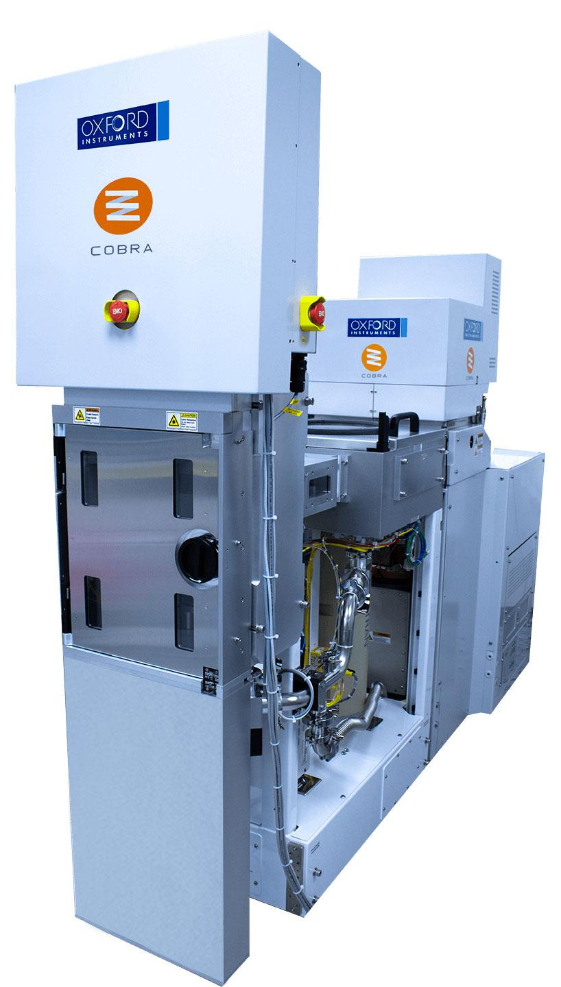
The plasma enhanced ALD system "AD-800LP" is a multi-purpose R&D system equipped with a unique ICP plasma source called "Tornado ICP", in addition to the conventional thermal ALD capability. AD-800LP enables various film deposition such as oxide or nitride films by Tornado ICP, which is Samco's proprietary plasma technology and is different from remote plasma. Tornado ICP enables stable plasma discharge even in the high-pressure range during ALD deposition.
“We are also considering a cluster ALD system that can connect multiple reaction chambers for production” says Tsukasa Kawabe, President and COO of Samco. “The launch of the AD-800LP will greatly enhance our presence in the world ALD equipment market.” Tsukasa adds.
As a global mid-sized company, Samco has successfully delivered numerous dry etch systems and plasma enhanced CVD systems for the electronic device field, mainly for compound semiconductors such as SiC, GaN, and GaAs, not only in Japan but also in the United States, Europe, Taiwan, Korea, China, Southeast Asia, India, and other countries.
The new Research Center for Nano Thin Films & Materials, which opened in February 2022, conducts research and development of unique thin film deposition, including ALD system. Samco will continue to utilize our "thin-film technology" to develop unique products and expand sales globally.
About Samco Inc.
Samco Inc. (TSE: 6387) stands for Semiconductor And Materials Company, and is a leading manufacturer of processing equipment for the semiconductor and related industries founded by Mr. Osamu Tsuji in Kyoto, Japan in 1979. Over the past forty-three years, more than 4,300 Samco systems have been installed and used in 35 different countries. Its equipment and thin film technology are widely adopted in the fabrication of semiconductor devices, including BAW filters, SiC power devices, GaN RF devices, GaAs VCSELs, InP lasers, microLEDs, MEMS, TSVs, advanced packaging, and so on. Learn more at https://www.samcointl.com/.