%20(1).png)
Continued scaling in semiconductor manufacturing increasingly relies on atomic-scale control of etching for complex 3D material stacks, making patterning precision a growing industrial bottleneck. Atomic layer etching (ALE) has emerged as a key enabler, with plasma-driven anisotropy and surface-chemistry control allowing improved selectivity and profile fidelity for advanced logic and memory integration. Current approaches emphasize decoupling surface modification from material removal to enable low-temperature, highly controlled processes.
From an industry perspective, the focus is shifting toward systematic ALE process development frameworks that combine thermodynamic screening, tailored half-cycle chemistries, and experimental verification of etch rates and selectivity. These strategies are increasingly relevant as device architectures push beyond conventional materials and dimensions. At the same time, ALE is gaining attention for its potential to reduce process complexity, energy use, and chemical consumption, positioning it as both a scaling and sustainability enabler for future semiconductor manufacturing.

In contrast, plasma ALE introduces ions as an active control parameter, most commonly during the removal step. A plasma first forms a chemically modified surface layer, such as a halogenated or oxidized film, which is then selectively removed by directional ion bombardment within a narrow ALE energy window. The momentum of the ions provides anisotropy, enabling vertical etching with atomic-scale precision while suppressing continuous sputtering. This directionality comes at the cost of tighter process windows and increased sensitivity to ion-induced damage.
A hybrid plasma–thermal ALE approach is presented as a way to decouple anisotropy from volatilization chemistry. In this scheme, plasma exposure is used to directionally modify the surface or precisely control the thickness of the modified layer, while removal proceeds via isotropic, thermally driven ligand-exchange reactions. This allows anisotropy to be engineered through selective surface modification rather than sputtering alone. Overall, the key conclusion is that isotropic versus directional behavior in ALE is determined by how and where ions are used, not simply by whether the process is labeled thermal or plasma.
Comment on Geometry
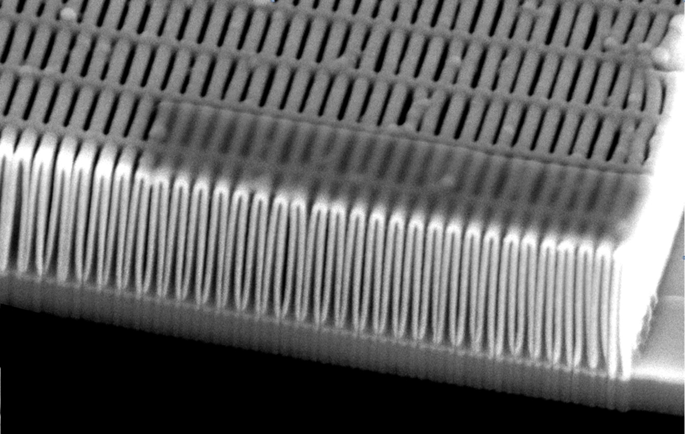
From an industrial standpoint, atomic layer etching is emerging as a core patterning technology as device scaling shifts toward complex 3D architectures and heterogeneous material stacks where conventional plasma etching reaches its limits. Smith et al. highlight that future adoption will be driven by selective ALE, enabled by surface-chemistry engineering, controlled anisotropy, and precise balance between etching and deposition rather than brute-force sputtering. In this landscape, AlixLabs’ use of geometrical selectivity extends the ALE paradigm by exploiting feature pitch and local geometry as an additional selectivity axis, enabling pattern multiplication and critical dimension scaling without added lithography complexity. The convergence of chemical, directional, and geometrical selectivity positions ALE not as a niche technique, but as a scalable, cost- and sustainability-aligned solution for next-generation semiconductor manufacturing.
The relevance of these advances is underscored by their recent and upcoming exposure at major industry forums. Results demonstrating sub-10 nm, high-aspect-ratio patterning with APS™ were presented at the 248th Electrochemical Society (ECS) Meeting in October 2025, marking an important milestone in validating the technology on bulk silicon using mature lithography. This momentum continues at SPIE Advanced Lithography + Patterning 2026, where AlixLabs will present new APS™ results spanning nanoimprint lithography and simplified self-aligned quadruple patterning, including joint work with UMC. Together, these events signal APS™ and geometrically selective ALE moving from concept and lab validation toward broader industrial evaluation and integration.


Reference:
Adapted from Smith, T. G. and Chang, J. P., Atomic Layer Etching in Patterning Materials: Anisotropy, Selectivity, Specificity and Sustainability, Plasma Chemistry and Plasma Processing, 46:9 (2026), © The Author(s) 2026. Published by Springer Nature and licensed under CC BY 4.0.