Thursday, December 17, 2015

Northwetsern and Argonne have synthesized Borophene

Borophene is a proposed crystalline allotrope of boron. Computational studies suggested that extended borophene sheets with partially filled hexagonal holes are stable. Borophene is predicted to be fully metallic and is analogous to graphene in that it is expected to form extended sheets. The latter is a semi-metal, implying that borophene may be a better conductor. The boron-boron bond is also nearly as strong as graphene’s carbon-carbon bond. [Wikipedia]
Borophene sheets. Image: Argonne National Laboratory
Now researchers at Northwestern University and Argonne National Laboratory have found an easy and inexpensive technique  to create borophene. Please check out the full details in the Science paper below.

Synthesis of borophenes: Anisotropic, two-dimensional boron polymorphs

Andrew J. Mannix et al
ScienceVol. 350 no. 6267 pp. 1513-1516, DOI: 10.1126/science.aad1080 

At the atomic-cluster scale, pure boron is markedly similar to carbon, forming simple planar molecules and cage-like fullerenes. Theoretical studies predict that two-dimensional (2D) boron sheets will adopt an atomic configuration similar to that of boron atomic clusters. We synthesized atomically thin, crystalline 2D boron sheets (i.e., borophene) on silver surfaces under ultrahigh-vacuum conditions. Atomic-scale characterization, supported by theoretical calculations, revealed structures reminiscent of fused boron clusters with multiple scales of anisotropic, out-of-plane buckling. Unlike bulk boron allotropes, borophene shows metallic characteristics that are consistent with predictions of a highly anisotropic, 2D metal.

Happy to welcome Beneq Oy as sponsors of The BALD ALD Blog!

A warm welcome to Beneq Oy of Finland - one of the new sponsors of the BALD Engineering ALD News Blog! You have already been hearing a lot of Beneq here and now you will hear even more! I visited the Beneq factory this summer in Finland and met with Beneq CEO Sampo Ahonen and his Team of ALD Experts and I was very impressed by their knowledge of ALD, the size of their facility and all ALD Products on display(!). Sampo has since then changed position in Beneq and is now Chairman of the Board.


Recently Beneq has started their own ALD Blog and you can follow their frequent news and articles here: http://www.beneq.com/blog


Workshop "Synchrotron Radiation to study Atomic Layer Deposition" 13th-15th June 2016

Workshop "Synchrotron Radiation to study Atomic Layer Deposition" 13th-15th June 2016. Save the date! For more information visit the page: https://indico.cells.es/indico/event/63/


The synchrotron facility ALBA, in Barcelona (Spain) and HERALD are organizing the first workshop on Synchrotron Radiation (SR) and ALD.

The high brilliance of a SR light source enables to study the atomic structure of matter as well as its properties. SR-based spectroscopic, scattering, and diffraction techniques are usually quiet fast and have a high degree of accuracy, precision and sensitivity. Therefore, they are very well suited to study ALD growth. However, until now, the use of SR to study ALD has remained a niche activity of a few groups, mostly because of technical obstacles, the limited availability of beam-time and/or issues concerning the use of certain precursors at synchrotron facilities. 

The workshop will take place at ALBA in June 2016 (more information here: https://indico.cells.es/indico/event/63/). Abstract submission will be opened in January 2016. Fee rates will be low for students, in order to facilitate their participation. 

For further information, please contact Massimo Tallarida (mtallarida@cells.es) and check the webpage (https://indico.cells.es/indico/event/63/).

Wednesday, December 16, 2015

LaAlO3/STO interface with a Chemically Switchable Ultraviolet Luminescence

A new effect discovered at Drexel University of a material stack that could be used to relay information between molecules by UV light like in a memory chip but with the significant advantage of doing it without an electric current.

"While studying a sample of lanthanum aluminate film on a strontinum titanate crystal, the team, led by Drexel College of Engineering Professor Jonathan E. Spanier, Andrew M. Rappe, from Penn; Lane W. Martin, from Berkeley and Temple's Xiaoxing Xi, discovered that the sample was beginning to emit intense levels of UV light. Carefully reproducing the experimental conditions helped them realize that water molecules might be playing a role in the UV light being emitted from inside the material."


In the presence of a water molecule on its surface, lanthanum aluminate film on a strontium titanate crystal emits ultraviolet light from its interior (Drexel University).

ALD 2016 Ireland Sponsorship and Exhibition

There are some fantastic opportunities for your organization or company for sponsoring the ALD 2016 and ALE 2016 in Dublin or take part in the exhibition this summer. Click here to download a copy of the ALD 2016 Ireland ‘Sponsorship and Exhibitor Facts Sheet’.

You may also contact:
Karen Hoey
Event Manager at Happening Events
ald@happeningcreative.com


Tuesday, December 15, 2015

ALD of III/V compound semiconductor GaAs using novel precursor chemistry from Helsinki

Here is a new ALD process for the III/V compound semiconductor GaAs from Laboratory of Inorganic Chemistry at Helsinki University (Prof. Leskelä & Prof. Ritala). GaAs has a zinc blende crystal structure and is used to manufacture devices such as microwave frequency integrated circuits, monolithic microwave integrated circuits, infrared light-emitting diodes, laser diodes, solar cells and optical windows. So a lot of military technology is based on this material.


Professor Markku Leskelä (on the left) and Professor Mikko Ritala are two of the most well-known names in the world of ALD research. Photo: Peter Herring (http://www.hightechfinland.com/direct.aspx?area=htf&prm1=1058&prm2=article)

However, GaAs is often used as a substrate material for the epitaxial growth of other III-V semiconductors including: Indium gallium arsenide, aluminum gallium arsenide and others that will be become very important channel material for sub 10 nm CMOS for transistors based on vertical and horizontal nano wires. So this paper is sort of back to the roots when ALD was called ALE as in Atomic Layer Epitaxy.

The main author Tiina Sarnet will be defending her Thesis "Non-metal Alkylsilyl Compounds as Precursors in Atomic Layer Deposition of Chalcogenides and Pnictides" on Monday next week, which you can find here:  Download file

John Morris Scientiffic distribution of Kurt J. Lesker's ALD 150LX


In this chamber cross section you can see how the Kurt J. Lesker engineers has solved the problem of protecting the windows for the elipsometer bz integrating a curtain gas distribution plate in the top chamber lid.

Monday, December 14, 2015

Imec Boosts Performance of III/V Devices using Novel ASMi ALD HKMG Stack

Imec presented a high performing gate-all-around InGaAs Nanowire FETs (Lg=50nm) at IEDM 2015. Imec succeeded in increasing the performance by gate stack engineering using a novel gate stack ALD inter-layer (IL) material developed by ASM, and high pressure annealing. The novel IL/HfO2 was benchmarked to the typically used Al2O3/HfO2 stack.

TEM of complete gate-all-around InGaAs Nanowire FET and HRTEM of the gatestack. The insert shows a close up of the Interface Layer HKMG developed and presumably deposited by ASM on any of the ASM ALD chambers available at imec - I am assuming that the high-k was deposited in a Pulsar 3000 and the TiN cap in a ASM A412 Large Batch ALD Furnace and I have absolutely no clue what the ALD inter layer may be - obviously it has less electrons than HfO2.

Beneq introduces new growth strategy and company structure – Jukka Nieminen appointed President

Press release from Beneq: Jukka Nieminen(46), M Sc (Tech), has been appointed President of Beneq Oy as of 1.1.2016. Sampo Ahonen (46), M Sc (Tech), who has since 2005 served as the CEO of Beneq, will continue as the Chairman of the Board.

 
Jukka Nieminen (left) and Sampo Ahonen (right).

The Board of Directors of Beneq Oy has also decided upon a plan to merge Beneq’s fully-owned subsidiary Beneq Products Oy with the mother company as of 1.1.2016. The combined entity Beneq Oy will have net sales of approximately 21 MEUR with a staff of 125 in Finland, the USA, Germany, Russia and China.

MIT Microscope creates near-real-time videos of nanoscale processes [VIDEO]

This would be cool to see tested in an ALD or ALE type process. MIT Reports on Youtube: Engineers at MIT have designed an atomic force microscope that scans images 2,000 times faster than existing commercial models.

Left to right, Fangzhou Xia, a new lab member who was not involved in the study; professor Kamal Youcef-Toumi; and postdoc Iman Soltani Bozchalooi.(Photo: Jose-Luis Olivares/MIT)

Saturday, December 12, 2015

MAM2016 & HERALD ALD for BEOL Workshop in Brussels March 20th

MAM 2016 will be the 25th in a series devoted to research on materials properties and interactions of interconnect and silicide materials.  Starting as a workshop on refractory metals and silicides in the 1980’s and moving towards materials for advanced metallization in 1995, the 2016 conference also aims to address new challenges in the fields of Materials for Flexible Electronics,


Korean ALD OEM NCD repeat order from Hyndai Heavy Industries

Korean ALD equipment manufacturer NCD reports repeat order from Hyndai Heavy Industries (HHI) for Al2O3 ALD passivation.

"NCD has recently contracted with HYUNDAI HEAVY INDUSTRIES(HHI) to supply 200MW of solar cell manufacture equipment which would be worth about 4million US dollars. The equipment is Lucida GS Series ALD system for high efficiency crystalline solar cell using Al2O3-ALD passivation to reduce surface defects on the rear side and then could get higher efficiency than normal soar cells. This equipment is the same model of previous supplied one at HHI as repeat order so it might be considered that the customer has confirmed the technology of NCD and the excellence in the equipment." Press release: http://www.ncdtech.co.kr/eng/index.html

The Lucida GS is a high throughput atomic layer deposition system for surface passivation of c-Si solar cells (ncdtech.co.kr)

Picosun's PICOPLATFORM™ ALD cluster tool with batch flipping mechanism

As you all know Santa Claus is operating out of North of Finland and he and his little helpers have busy times right now to fulfill everyone wishes for Christmas. To help in a bit on the way Picosun has developed a ALD Batch Tool with an amazing batch flipping loading mechanism. Yeah that´s right a fully automatic ALD cluster tool running ALD Batch processes!


Below is a video showcasing the ALD Batch Cluster Tool with the Flip laoding mechanism and there are many more videos from Picosun to look at here : http://www.picosun.com/en/media/videos/

Thursday, December 10, 2015

Imec owned IEDM 2015 and presented 23 papers

Imec seemed to have owned IEDM 2015 and presented 23 papers 2015. Woah! I remember some years ago they "only" presented 11 papers. Imec also organized a Imec Technology Forum - a meeting – by invitation only – that took place December 6 at the Belgian Embassy in Washington

I am extremely proud with the record number of 23 papers that we present at this year’s IEDM2015. Our presence rewards and confirms our leading position in advanced semiconductor R&D. As much as 10 of the presented papers concerned the different aspects of our advanced logic program.

Next to our research efforts to extend silicon CMOS technology into 7nm technology node and beyond. We are looking into beyond silicon CMOS, integrating high mobility materials to increase the channel mobility, and explore new concepts beyond silicon such as spintronics and 2D materials.
Luc Van den hove - President and CEO, imec

Many papers - So I will need to dig into this in more detail... I'll be back.


Stanford skyscraper chip design boosts electronic performance by factor of a thousand

Americans love building Skyscrapers and now they will get going building Skyscraper chips. They also like using units for temperature that nobody can relate to - it must be the first time I hear somebody using Fahrenheit referring to thermal budget in CMOS processing. 

"Fabricating a silicon chip requires temperatures close to 1,800 degrees Fahrenheit, making it extremely challenging to build a silicon chip atop another without damaging the first layer. The current approach to what are called 3-D, or stacked, chips is to construct two silicon chips separately, then stack them and connect them with a few thousand wires." 


A multi-campus team led by Stanford engineers Subhasish Mitra and H.-S. Philip Wong has developed a revolutionary high-rise architecture for computing. (Stanford University)

The limits of ALD barrier seed for Cu metallization

Here is a great piece by ED KORCZYNSKI, Senior Technical Editor at Solid State Technology on the practical limits for metallization beyond 14nm tthat inspired me too dig into ALD Mn self forming barriers.


Ed states that one of the limitation for Cu metallization will actually be how thin you can deposit an ALD barrier/seed layer (see figure below).


Tuesday, December 8, 2015

#VPHA - Update of Wikipedia Atomic Layer Deposition page

To update Wikipedia pages is one of the VPHA publication plan outcomes listed for VPHA (#11, http://vph-ald.com/Publication%20Plan.html).


There are a lot of missing info and some errors as noted by Riikka Puurunen blog post in the ALD History Blog, http://aldhistory.blogspot.fi/2015/12/ald-in-wikipedia-status-and-surprises.html.

Please let us, Jonas Sundqvist and Angel Yanguas-Gil, know if you are interested to contribute since we have volunteered to lead the Wikipedia update activities.

Monday, December 7, 2015

Yet another novel phase of carbon - Q-carbon

Ta da! So there is yet another phase of carbon available - Q-carbon! In the light of C60, carbon nano tubes (CNTs) and graphene, it will for sure be exiting to follow the development of this discovery. For a starter the Q-carbon exhibits robust bulk ferromagnetism with estimated Curie temperature of about 500 K, which may come handy for all sort exiting materials.

Bellow are two publications by Jagdish Narayan and Anagh Bhaumik from at North Carolina State University.


The gentlemen behind the discovery - Jagdish Narayan and Anagh Bhaumik. Lets assume that they will be awaiting a phone call from Stockholm the next years.  (Photos from Research Gate profiles)

Novel phase of carbon, ferromagnetism, and conversion into diamond

Jagdish Narayan and Anagh Bhaumik
J. Appl. Phys. 118, 215303 (2015); http://dx.doi.org/10.1063/1.4936595


We report the discovery of a new phase of carbon (referred to as Q-carbon) and address fundamental issues related to direct conversion of carbon into diamond at ambient temperatures and pressures in air without any need for catalyst and presence of hydrogen. The Q-carbon is formed as result of quenching from super undercooled state by using high-power nanosecond laser pulses. We discuss the equilibrium phase diagram (P vs. T) of carbon and show that by rapid quenching kinetics can shift thermodynamic graphite/diamond/liquid carbon triple point from 5000 K/12 GPa to super undercooled carbon at atmospheric pressure in air. It is shown that nanosecond laser heating of diamond-like amorphouscarbon on sapphire, glass, and polymer substrates can be confined to melt carbon in a super undercooled state. By quenching the carbon from the super undercooled state, we have created a new state of carbon (Q-carbon) from which nanodiamond, microdiamond, microneedles, and single-crystal thin films are formed depending upon the nucleation and growth times allowed for diamond formation. The Q-carbon quenched from liquid is a new state of solid carbon with a higher mass density than amorphouscarbon and a mixture of mostly fourfold sp3 (75%–85%) with the rest being threefold sp2 bonded carbon (with distinct entropy). It is expected to have new and improved mechanical hardness, electrical conductivity, chemical, and physical properties, including room-temperature ferromagnetism (RTFM) and enhanced field emission. Here we present interesting results on RTFM, enhanced electrical conductivity and surface potential of Q-carbon to emphasize its unique properties. The Q-carbon exhibits robust bulk ferromagnetism with estimated Curie temperature of about 500 K and saturation magnetization value of 20 emu g−1. From the Q-carbon, diamond phase is nucleated and a variety of micro- and nanostructures and large-area single-crystal diamond sheets are grown by allowing growth times as needed. Subsequent laser pulses can be used to grow nanodiamond into microdiamond and nucleate other nanostructures of diamond on the top of existing microdiamond and create novel nanostructured materials. The microstructural details provide insights into the mechanism of formation of nanodiamond, microdiamond, nanoneedles, microneedles, and single-crystal thin films. This process allows carbon-to-diamond conversion and formation of useful nanostructures and microstructures at ambient temperatures in air at atmospheric pressure on practical and heat-sensitive substrates in a controlled way without need for any catalysts and hydrogen to stabilize sp3 bonding for diamond formation.

Research Update: Direct conversion of amorphous carbon into diamond at ambient pressures and temperatures in air

J. Narayan , A. Bhaumik
APL Materials  10/2015; 3(10):100702. DOI: 10.1063/1.4932622

ABSTRACT
We report on fundamental discovery of conversion of amorphous carbon into diamond by irradiating amorphous carbon films with nanosecond lasers at room-temperature in air at atmospheric pressure. We can create diamond in the form of nanodiamond (size range <100 nm) and microdiamond (>100 nm). Nanosecond laser pulses are used to melt amorphous diamondlike carbon and create a highly undercooled state, from which various forms of diamond can be formed upon cooling. The quenching from the super undercooled state results in nucleation of nanodiamond. It is found that microdiamonds grow out of highly undercooled state of carbon, with nanodiamond acting as seed crystals.


ASMi to host Technology Seminar at IEDM with Dina Triyoso from Globalfoundries

ASM International, the leading supplier of ALD deposition tools for leading edge Logic and Memory technologies is as usual hosting a Technology Lunch Seminar at IEDM that is taking place this week in Washington. This time they have invited Dina Triyoso from Globalfoundries to give a talk on

'Architectural choices and material challenges for future electronics'. Dina has a very strong background in ALD, High-k/Metal Gate, MIM capacitors and ALD for spacer technologies so this will certainly be a fantastic opportunity to learn about the latest from a true expert in the field.


ASM International N.V. (Euronext Amsterdam: ASM) today announces that it will host a technical luncheon seminar in Washington DC, US, on Wednesday, December 9, 2015, the third day of the IEDM Conference.

In this technology seminar, ASM and a distinguished keynote speaker will highlight the challenges and potential solutions for achieving next generation 3D devices.

The agenda is as follows:

11:30 am Food and drinks
12:10-12:20 pm Ivo Raaijmakers (ASM) - Welcome and introduction
12:20-12:50 pm Dina Triyoso (GLOBALFOUNDRIES) -
'Architectural choices and material challenges for future electronics '

Following the presentations, there is an opportunity for open discussion and networking until 1:15 pm.

The ASM technology seminar will take place in the Kalorama room at the Churchill Hotel (across from the Hilton Washington), 1914 Connecticut Avenue NW, Washington DC 20009, US. The room will open at 11:30 am for invited attendees. Interested parties should contact Rosanne de Vries, +31 88 100 8569, rosanne.de.vries@asm.com.

Source: http://www.finanznachrichten.de/nachrichten-2015-12/35815943-asm-international-nv-asm-international-n-v-to-host-technology-seminar-399.htm

Sunday, December 6, 2015

Ultralight shape-recovering plate mechanical ALD metamaterials

Here is an Ultracool ALD application for creating Ultralight shape-recovering plate mechanical  metamaterials from University of Pennsylvania. Check out the paper and the Youtube video below. 


Sequential images of a structure with the ALD layer thickness of ~25 nm inside an FIB while being manipulated using a micromanipulator. (Nature Communications 6, Article number:10019 doi:10.1038/ncomms1001)

All details on the fabrication method can be found in the supplementary information document with free access: http://www.nature.com/ncomms/2015/151203/ncomms10019/extref/ncomms10019-s1.pdf

And the paper itself is OPEN ACCESS !


Fabrication method of the periodic three-dimensional architecture of the mechanical metamaterial as described in the supplementary information document (Nature Communications 6, Article number:10019 doi:10.1038/ncomms1001)

Ultralight shape-recovering plate mechanical metamaterials

Keivan Davami, Lin Zhao, Eric Lu, John Cortes, Chen Lin, Drew E. Lilley, Prashant K. Purohit & Igor Bargatin

Nature Communications 6, Article number:10019 doi:10.1038/ncomms10019 Published 03 December 2015 

Unusual mechanical properties of mechanical metamaterials are determined by their carefully designed and tightly controlled geometry at the macro- or nanoscale. We introduce a class of nanoscale mechanical metamaterials created by forming continuous corrugated plates out of ultrathin films. Using a periodic three-dimensional architecture characteristic of mechanical metamaterials, we fabricate free-standing plates up to 2cm in size out of aluminium oxide films as thin as 25nm. The plates are formed by atomic layer deposition of ultrathin alumina films on a lithographically patterned silicon wafer, followed by complete removal of the silicon substrate. Unlike unpatterned ultrathin films, which tend to warp or even roll up because of residual stress gradients, our plate metamaterials can be engineered to be extremely flat. They weigh as little as 0.1gcm−2 and have the ability to ‘pop-back’ to their original shape without damage even after undergoing multiple sharp bends of more than 90°.


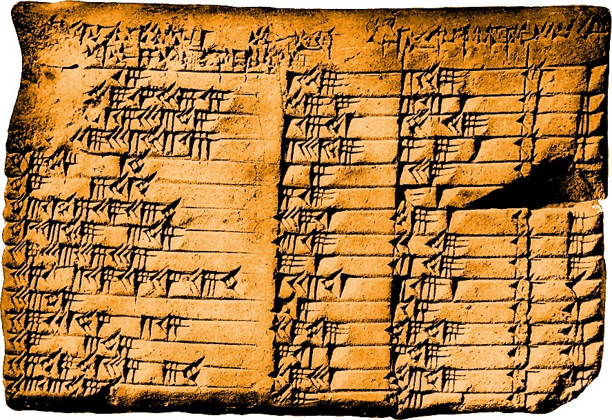
NEWS FLASH! The Babylonians to suit Apple for use of rounded corners

NEWS FLASH! The Babylonians to suit Apple for use of rounded corners

The Plimpton 322 tablet is a Babylonian clay tablet, written in cuneiform, from around 1,800 BC (now held at Columbia University). The tablet contains four columns of numbers, written in base 60 (a system that survives in our hours, minutes, and seconds):

The Babylonian Clay Tablet Plimpton 322 before Iphone & Ipad 1,800 BC.

A close up of a rounded corner.


Russian Comberry is offering Combinatorial ALD development from Intermolecular HPC platform


Comberry, a Russian based joint venture with Intermolecular that started in 2013 is offering combinatorial materials development on one of the coolest ALD tools ever built - The Tempus AP-30 Vacuum Cluster. This tool is part of a large HPC platform including also PVD, CVD and wet chemistry.


Tempus® AP-30 Vacuum Cluster Module

This is the main module that utilizes wafers up to 300 mm in diameter. It is equipped with several (up to 5) ALD and PVD chambers as well as pre-clean and degassing modules and allows for fast deposition of various, isolated, thin-film samples by ALD and PVD methods without interrupting vacuum between technological processes.


Vacuum cluster module Tempus® AP-30


Comberry promotional video in Russian with English subtitles.

Comberry (Comberry, LLC), a Technology Company

 Comberry was established, by the Nanocenters of Dubna, Ulyanovsk and Saransk jointly with Intermolecular Inc., in October 2013 Intermolecular, Inc.

Product:
- applied research in the field of multifunctional thin-film coatings for various materials.


Comberry mission: to provide innovative Russian companies with technological development capabilities, poised to allow them to become successful producers of high-tech products.

Joint development projects make it possible for Comberry’s customers to increase the efficiency of applied research and create large numbers of intellectual property objects while reducing the time to market for new products

First stage projects:
  • Transparent Conductive Oxides
  • Electrochromic devices
  • Flexible, thin-film, copper-indium-gallium selenide solar cells (CIGS)

Saturday, December 5, 2015

Samsung is using an ALD Al2O3 gate dielectric for 3D V-NAND

Samsung seems to be using an ALD Al2O3 gate dielectric with a TiN/W Metal Gate according to Dick James at Chipworks who recently reported on the matter in front of IEDM 2015 (http://electroiq.com/chipworks_real_chips_blog/2015/12/02/a-look-ahead-at-iedm-2015/).

"Samsung started shipping their V-NAND last year, but that uses charge-trap storage, in which the electrons that make up the memory bits sit on a silicon nitride layer; the Intel/Micron device uses the conventional floating-gate method used in planar flash, where the electrons are stored on a polysilicon floating gate. It’ll be interesting to see the difference!"

Plan-view TEM images of Samsung V-NAND flash array (Chipworks) 

Looking at the rest of the stack one want to believe that also the TiN, SiO2 and SiN is deposited by ALD. However, knowing that those materials can successfully be deposited in a LPCVD or pulsed LPCVD process it can just as well be done in Large Batch furnaces from any of the companies ASM, Kokusai or Tokyo Electron. Those furnaces are for sure also capable of running the processes in a pure ALD mode though.

Below is a principal cross section of the first couple of cells in the Samsungs 3D NAND  from
Samsung SSD 850 Pro (128GB, 256GB & 1TB) Review: Enter the 3D Era by Kristian Vättö"


"NAND scaling in vertical dimension does not have the same limitations as scaling in the X and Y axes do. Because the cost of a semiconductor is still mostly determined by the die area and not by the height, there is no need to cram cells very close to each other. As a result, there is very little interference between the cells even in the vertical direction. Also, the usage of high-k dielectrics means that the control gate does not have to wrap around the charge trap. The result is that there is a hefty barrier of silicon dioxide (which is an insulator) between each cell, which is far more insulating than the rather thin ONO layer in 2D NAND."

Friday, December 4, 2015

Picosun & ALD - Enabling Future Industries

Here is a new Winter issue of the Picosun magazine covering the latest developments in this ever expanding ALD company from Finland - Born in Kirkkonummi, Born to ALD and as you know Santa comes from Finland and that´s why there are only stone hard gifts for Christmas.


In this issue:
• PICOPLATFORM™ vacuum cluster tools solidify their presence in industrial
ALD market
• Picosun provides batch ALD technology for medical and aerospace electronics
• PICOPLASMA™ technology paves the way for future microelectronics
• Picosun hires new professionals to lead foreign operations

Customer interviews:
• Prof. Paul R. Berger, USA
• Dr. Peter King, United Kingdom
• Dr. Kaushal Vora and Dr. Fouad Karouta, Australia


Meaglow - Optimum Plasma Source to Substrate Distance

Here is a recent white paper from Meaglow on plasma source substrate distance optimization.

What is the optimum distance to the substrate?

This question is frequently asked by Meaglow customers. The short answer is: if you’re replacing an existing ICP source with a Meaglow hollow cathode, then using the same distance will be appropriate. Using the same distance will give you results that will allow you to compare the advantages of your hollow cathode source. The same operating conditions can be used, though there may be changes in the growth per cycle, and improvement in the quality of the material - the extent of which will be material dependent. The long answer is: the optimum distance is dependent on a number of variables. Plasma gas type, the material being deposited, the metalorganics used, the gas pressure, the power  applied to the plasma source and the flow rate from the plasma  source, all interact to determine this value. Some guidelines can be provided. Generally there are two  overriding considerations: delivery of a high flux of active species  to enhance growth rate, versus the damage that the material being deposited can sustain.

Improved Corrosion Resistance of CrN Hard Coatings with an ALD Al2O3 Interlayer

As mentioned in the previous post  - Han-Bo-Ram Lee research group at the Nanomaterials Laboratory of  Incheon National University Korea has a nice blog/news service where they publish all recent results on regular basis.


Here I found this paper on using ALD interlayers for CrN corrosion protection coatings

[Paper]Improved Corrosion Resistance and Mechanical Properties of CrN Hard Coatings with an Atomic Layer Deposited Al2O3 Interlayer

image


Zhixin Wan, Teng Fei Zhang, Han-Bo-Ram Lee, Ji Hoon Yang, Woo Chang Choi, Byungchan Han, Kwang Ho Kim,and Se-Hun Kwon

ACS Appl. Mater. Interfaces, Article ASAP
DOI: http://pubs.acs.org/doi/pdf/10.1021/acsami.5b08696

Abstract

A new approach was adopted to improve the corrosion resistance of CrN hard coatings by inserting a Al2O3 layer through atomic layer deposition. The influence of the addition of a Al2O3 interlayer, its thickness, and the position of its insertion on the microstructure, surface roughness, corrosion behavior, and mechanical properties of the coatings was investigated. The results indicated that addition of a dense atomic layer deposited Al2O3 interlayer led to a significant decrease in the average grain size and surface roughness and to greatly improved corrosion resistance and corrosion durability of CrN coatings while maintaining their mechanical properties. Increasing the thickness of the Al2O3 interlayer and altering its insertion position so that it was near the surface of the coating also resulted in superior performance of the coating. The mechanism of this effect can be explained by the dense Al2O3 interlayer acting as a good sealing layer that inhibits charge transfer, diffusion of corrosive substances, and dislocation motion.

2X Korean ALD News Blogs from CN1 and Incheon National University

So today I was reading some papers and found an interesting one on selective Co CVD using the market leading precursor CoCOCp [CoCp(CO)2]. The paper was recently published by a Korean research group at Incheon National University and as usual I went digging up the facts what hardware was being used and then I find this Korean ALD equipment compoany CN1 that I have scouted before. Anyway, they have updated their web and have a nice news blog and especially nice to find that they sometimes link to my blogs.


Check it out, there are mixed news in English and Korean.: http://www.cn-1.co.kr/about-us/news/

Atomic Premium  - Showerhead type Plasma-Enhanced ALD (PE-ALD) cluster tool from CN1


...and by the way here is that Co paper - Open Source - and the Nanomaterials Lab of Incheon National University  also have a News Blog : http://nanomaterial.kr/


ALD History Blog: List of ALD reviews

ALD History Blog: Another page under construction: List of ALD revie...: A list of scientific reviews (including books) on ALD is now under construction as a separate page in the ALD History Blog: http://aldhistory.blogspot.fi/p/list-of-reviews.html.

This initial list, started December 3, 2015, contains the list of reviews collected for my (Puurunen's)  review articles in J. Appl. Phys. 2005 and 2013, with some items added for years 2012 on.


Wednesday, December 2, 2015

The Colors of Reliability - The ALD Displays from Finland

Lumineq® Displays, a business unit of Beneq, a manufacturer and developer of thin film electroluminescent (TFEL) displays. Lumineq TFEL non-transparent displays are used in mining, marine, military, medical and many more demanding environments. TFEL displays are robust and reliable, and usually used in extreme environments, where traditional displays cannot cope with the conditions.


The black and yellow colors are inherent for thin film electroluminescent displays because of the technology (a ZnS:Mn phospor layer is the most efficient and its emissions are seen as yellow by the human eye), but we have been told that they are sometimes copied in demos of other display technologies to represent reliability. So strong is the mental connection between these colors and robustness for those in the business.
 
Read mor at the Beneq Blog : http://www.beneq.com/colors-of-reliability

Tuesday, December 1, 2015

Samsung to present low cost manufacturing of 20 nm DRAM and beyond at IEDM2015

Some advancement in keeping low cost manufacturing of 20 nm DRAM will be presented by Samsung at IEDM 2015. Key elements are:

  • avoiding EUV lithography
  • honeycomb structure (see figure below)
  • air-spacer technology


According to Solid State Technology an air-gap spacer arrangement achieves a 34% reduction in bitline capacitance for faster operation.

20nm DRAM: A New Beginning of Another Revolution (Invited), J. Park, Y.S. Hwang, S.-W. Kim, S.Y. Han, J.S. Park, J. Kim, J. W Seo, B.S. Kim, S.H. Shin, C.H. Cho, S.W. Nam, H.S. Hong, K.P. Lee, G.Y. Jin, and E.S. Jung, Samsung Electronics Co.


For the first time, 20nm DRAM has been developed and fabricated successfully without EUV lithography using the honeycomb structure and the air-spacer technology. These low-cost and reliable schemes are promising key technologies for 20nm technology node and beyond.