%20(1).png)
ESPOO, Finland, 30th August, 2016 – Picosun Oy, the leading supplier of advanced Atomic Layer Deposition (ALD) manufacturing solutions, partners with A*STAR’s Institute of Microelectronics (IME) in Singapore and global, prominent semiconductor industries to develop next generation chip packaging technology.
.jpg)
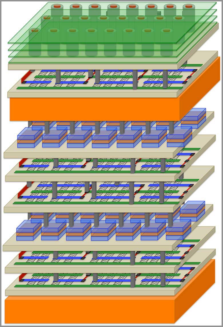
A*STAR 2.5D interposer Multi-Project Wafer supported by state-of-the-art Through-Silicon Via (TSV) engineering lines in both 200mm and 300mm [A*STAR]
Higher and higher performance, speed, multifunctionality, reliability, and compact size are required from today’s microelectronics, to answer the customers’ demands, while the manufacturing costs must remain low to retain competitiveness.
The Cost-Effective Interposer Consortium brings together frontline semiconductor manufacturers and research institutes to address these challenges. Picosun joins forces with e.g. IME, Inotera Memories, STATS ChipPAC Pte. Ltd., Teradyne Corporation, Tessolve Semiconductor Pvt. Ltd., UMC, and Veeco Instruments to develop advanced, high volume manufacturing solutions for cost-efficient packaging of the chip components.
“We are happy to have Picosun as a member in the Cost-Effective Interposer Consortium. This collaborative partnership will harness the expertise of our partners, including Picosun’s strong know-how in ALD, and IME’s deep R&D experience to accelerate the development and time-to-market of cost-efficient next-generation electronic devices,” says Prof. Dim-Lee Kwong, Executive Director of IME.
“ALD is a central manufacturing method in today’s semiconductor industries, and the very technology that enables the future developments in the field. For Picosun, this is clearly our most important market area, where several world-leading IC industries already rely on our production-proven ALD solutions. We are excited to collaborate with such a number of prominent microelectronics industries and our long-time partner and valued customer, IME, in the Cost-Effective Interposer Consortium,” states Juhana Kostamo, Managing Director of Picosun.
A central approach to solve many key challenges in modern microelectronics development is wafer-level 3D-integration of the components, which enables continued downscaling of the chip size while retaining high performance and reliability. Cost savings are obtained when larger number of chips can be manufactured on the same wafer. ALD is a key technology to realize the ultra-thin active layers crucial for the chip component functionality, such as high-k dielectrics for MIM (metal-insulator-metal) capacitors and high aspect ratio liners.