Monday, April 8, 2019

Meaglows New Hollow Cathode Plasma Source Designs Provide Better Quality Films

The University of Connecticut group of Dr. Necmi Biyikli, with others, have recently published a paper (J. Vac. Sci. and Technol. A 37 (2019) 020927) where they were able to achieve good quality, highly stoichiometric AlN using hollow cathode plasma-assisted atomic layer deposition (HCPA-ALD) with film densities near bulk values. Because of the high radical flux from the source, significantly lower RF power was required to achieve this improvement in material quality compared to past experience, and shorter plasma on cycles could be used at these lower powers (20 seconds at 100 watts compared to 40 seconds at 300 watts).

0.125 sec exposure 278 watt 4130 mTorr

Similar improvements in silicon nitride deposition were recently achieved by a team at the University of Texas, Dallas, where excellent quality, highly stoichiometric, high-density PA-ALD grown material was performed using one of our hollow cathode plasma sources (see, for instance, IEEE Electron Device Letters 39 (2018) 1195 ).

IMG_9895

The image shows the University of Connecticut plasma source with ellipsometer ports and sample entry door. The 4″ diameter source was custom made for use with an Okyay Tech ALD system.

Meaglow’s hollow cathode plasma sources are widely used by the ALD Research Community as replacements for inductively coupled plasma (ICP) sources because there is less oxygen contamination when depositing non-oxide materials. However, these recent papers, by the University of Connecticut and the University of Texas, Dallas, illustrate advantages that may be far more important for the industry moving forward. Those being an extremely high radical flux, to the point where the ion signal (ion densities are similar to ICP sources) is swamped by the signal of radicals during optical emission spectroscopy measurements, and relatively low plasma damage (see our company white paper on hollow cathode sources). These result in quicker deposition times with potentially more stoichiometric, better quality material.

Saturday, April 6, 2019

Amtech Systems plans to divest its solar businesses


Amtech Systems, a manufacturer of capital equipment and consumables used in fabricating semiconductor devices, LEDs, SiC and silicon power chips ans well as solar cells, is planning to sell its solar businesses.

Amtech management and Board of Directors have decided to focus solely on growth opportunities in the Company’s semiconductor and SiC/LED polishing businesses and intend to sell the Company’s solar businesses, including its Tempress and SoLayTec subsidiaries. 

Amtech’s J.S. Whang, Chairman and Chief Executive Officer, commented, “In November 2018 we announced that we had initiated a comprehensive review of our solar businesses.  In a February update we noted thus far our review strongly indicates that our combined Semi and SiC/LED polishing business provide better markets for enhancing the value of Amtech Group. We have recently completed our assessment and conclude, along with Tempress and SoLayTec management, that significant investment is required to effectively compete in the changing solar industry. We therefore conclude Tempress and SoLayTec would be better positioned to capitalize on opportunities in the solar industry under new ownership.”
 
Source: Evertiq LINK

Thursday, April 4, 2019

Yes! The ALD/CVD Paper bot on Twitter is activated!

Yes! The ALD/CVD Paper bot on Twitter is activated! 68 Tweets (Papers) and counting.

@CVD_ALD_papers
I'm a paper bot surveying publications covering CVD & ALD! Operated by @DennisZyw93 & @Semajobe (Ruhr University). Adapted open-source code from @fxcoudert.


Applied Optoelectronics orders MOCVD technology from AIXTRON

Photonics manufacturer expands production into growing laser business with multiple AIX 2800G4 systems

Herzogenrath/Germany, 2 April, 2019 – AIXTRON SE (FSE: AIXA), a worldwide leading provider of deposition equipment to the semiconductor industry, today announced the delivery of multiple AIX 2800G4 systems to US-based photonic maker Applied Optoelectronics, Inc. (AOI) which focuses on the design, development, and manufacturing of advanced optical devices, packaged optical components, optical subsystems, laser transmitters, and fiber optic transceivers. The delivered tools feature a 12x4-inch configuration.

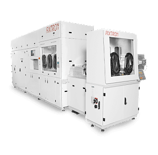
AIX 2800G4-TM

The AIX 2800G4 platform has established itself as the market-leading tool for high-volume production of vertical-cavity surface-emitting lasers (VCSEL) for 3D sensors and other diode lasers due to the matchless performance of the Planetary Reactor® concept with respect to thickness and wavelength uniformity control of epitaxial layers. The system provides incomparably high efficiency in handling the expensive chemicals used for MOCVD processes while delivering maximum production yield of premium level laser devices. In addition to the excellent reproducibility of each individual system, customers also appreciate the very good repeatability amongst systems.

Dr. Klaus Anselm, Vice President of Semiconductor Products at AOI, comments: "Following our good experience with AIXTRON systems in the past, we will also utilize the proven Planetary® technology from Germany for our production expansion. The AIX 2800G4 has convinced us in all test phases, so that we are now looking forward to use the system for launching volume production of our next generation of optoelectronic components."

"We are very pleased that AOI has added our market-leading AIX 2800G4 tool to its existing manufacturing equipment. A system that has acquired a reputation over the past few years as the tool of record for the production of high-quality laser devices in the semiconductor industry. We are looking forward to the collaboration with AOI," says Dr. Bernd Schulte, President of AIXTRON SE.

Wednesday, April 3, 2019

Ionbond Equipment Division integrated into IHI Hauzer Techno Coating

Ionbond is pleased to announce the sale of its equipment division to fellow IHI Group company Hauzer Techno Coating.

Under Hauzer, which produces physical vapor deposition (PVD) equipment for the tribological, tool and decorative market, the equipment division will continue as an indpendent company under the name IHI Bernex. IHI Bernex will continue to work closely with the Ionbond group on key projects and developments. 

Maximize strength by expansion
Dave Doerwald, Hauzer CEO: “The Bernex portfolio is an excellent complement to the Hauzer portfolio, allowing the two companies to serve more customers together. We are both equipment manufacturers and speak the same language when it comes to doing business.” Dr. Michael Auger, Bernex CEO, adds: “Bernex is profitable and growing, and we are looking forward to the synergies that will come from working with Hauzer. Both companies have a lot to offer.”

The integration of the Ionbond equipment division into Hauzer is in line with the aim of the IHI Group to maximize synergies by aligning equipment production activities. “  Bernex will be an independent company within the Hauzer group, with the same people and the same business location in Olten, Switzerland. 


Leader in CVD Solutions
Bernex CVD systems set the industry standard in CVD enhancement of wear, friction and temperature protection of tools and components. Bernex machines are renowned for their reliability and have proven themselves in hundreds of installations worldwide. The company has over 45 years of experience with developing technology, equipment and recipes for CVD coatings. Auger: “CVD is in our DNA. We have expanded CVD technology to include CVA (for aluminum coatings) and CVI (for coating the internal surfaces of porous materials such as carbon fiber bodies). Our expertise in developing proprietary coatings for specific customer applications sets Bernex apart in the field.”

Bernex Expanding Production Capacity
Bernex engineering and manufacturing will remain in Olten, where it is expanding its production capacity. The Bernex Service Center Asia will remain in Kunshan, China.

For more information, see the new Bernex website: ihi-bernex.com

Shared by: Prof. Pedersen

VEECO Demonstrates Thought Leadership at Technical Conferences in 2Q/2019


Company’s Technologists to Present Innovations that Drive Industrial Scaling of Technology Megatrends in Big Data, Artificial Intelligence, Communications, Autonomous Vehicles, Displays and More

PLAINVIEW, New York, April 2, 2019—Veeco Instruments Inc. (Nasdaq: VECO) today announced its leading technologists are scheduled to speak at seven technical events throughout Q2 2019. The forthcoming presentations, which follow several notable appearances in Q1, highlight Veeco’s depth and breadth of expertise in working with customers to break through production-scale barriers that will ultimately lead to the wide adoption of game-changing trends in big-data, high-speed communications, artificial intelligence, autonomous vehicles, high resolution displays and more.

Veeco exhibiting and presenting at EFDS ALD for Industry (March 19-20; Berlin, Germany) “Atomic Layer Deposition Use for Decorative Applications” Ganesh Sundaram, Ph.D., vice president of Applied Technology, Veeco CNT. (Photo by Martin Knaut LINK)

Through these papers, Veeco explains how it solves tough materials engineering challenges with advances in its deposition, etch, lithography and wet processing technologies used in applications such as next-generation advanced packaging, photonics, sensors, MEMS, micro-LEDs, power electronics, high bandwidth memory and related devices. Presentations in the second quarter include:

  • MRS Spring Meeting & Exhibit (April 22-26; Phoenix, AZ)—Tania Henry, process development engineer, will present “Influence of Intermixing on Perpendicular Magnetic Anisotropy of Ion-Beam-Deposited CoFeB MTJs for STT-RAM,” on April 25 during the annual meeting focused on the future of materials science
  • Critical Materials Council Conference (April 25-26; Saratoga Springs, NY)—Drew Hanser, vice president of technology, will present at the fourth annual forum for discussing actionable information related to semiconductor fab materials. Hanser’s talk, “Material Integration Challenges for GaN on Si for Power and RF Devices,” takes place on April 25 during Session II: Immediate Challenges of Materials & Manufacturing
  • Society of Vacuum Coaters TechCon (April 27-May 2; Long Beach, CA)—At one of the world’s leading vacuum coating technology conferences, senior research scientist Binyamin Rubin will discuss “Monochromatic and Broadband Optical Monitoring for Deposition of Band Pass Filters,” on April 29. The Veeco team will also be exhibiting its latest advances in ion beam deposition systems for optical coatings at booth #229
  • CS ManTech (April 29-May 2; Minneapolis, MN)—Phillip Tyler, process development engineer, will present “Development of Advanced Lift Off Processes for 5G and VCSEL Applications.” Stop by Veeco’s booth #609 to learn more about the company’s latest innovations in compound semiconductor and wet processing technologies
  • ECTC (May 28-31; Las Vegas, NV)—Dr. Ajit Paranjpe, chief technology officer, will co-author a presentation on “High-Yield Precision Transfer and Assembly of Gallium Nitride (GaN) Micro-LEDs Using Laser Assisted Micro Transfer Printing,” with experts from the University of California, Los Angeles
  • EUVL Workshop (June 10-13; Berkeley, CA)—At this year’s workshop focused on the fundamental science of EUV lithography and its continued extension to support Moore’s Law, Sandeep Kohli, principal research scientist, will present “Ion Beam Technology Roadmap for EUV Mask Deposition and Absorber Etch Processes”
  • TechConnect World Innovation Conference and Expo (June 17-19; Boston, MA)—Dr. Ganesh Sundaram, vice president of applied technology, will present “Atomic Layer Deposition for Life Science Applications” on June 17 at the Nanomedicine Symposium
Veeco scientists also presented research at a number of key technical conferences in Q1, including:
  • SPIE Advanced Lithography (Feb. 24-28; San Jose, CA)
    • “Ion Beam Etching of Advanced Absorber Materials for Sub-5nm EUV Masks”
    • “Intra-field Stress Impact on Global Wafer Deformation” (alongside ASML and imec)
  • EFDS ALD for Industry (March 19-20; Berlin, Germany)
    • “Atomic Layer Deposition Use for Decorative Applications”
  • CS International (March 26-27; Brussels, Belgium)
    • “Accelerating Photonics Growth through Advances in High-Performance Arsenic/Phosphide (As/P) MOCVD and Wet Processing Technology”
“Veeco builds production-scale fab solutions that solve tough materials engineering problems for our customers,” said Ajit Paranjpe, Ph.D., chief technology officer. “Our technical contributions to these prestigious and peer-reviewed conferences demonstrate Veeco’s commitment to remaining at the forefront of technological advances, which ultimately have a positive impact on society through life-improving applications.”

About Veeco

Veeco (NASDAQ: VECO) is a leading manufacturer of innovative semiconductor process equipment. Our proven MOCVD, lithography, laser annealing, ion beam and single wafer etch and clean technologies play an integral role in producing LEDs for solid-state lighting and displays, and in the fabrication of advanced semiconductor devices. With equipment designed to maximize performance, yield and cost of ownership, Veeco holds technology leadership positions in all these served markets. To learn more about Veeco's innovative equipment and services, visit www.veeco.com.

Tuesday, April 2, 2019

RASIRC to Highlight Precise Water Vapor Delivery in Area Selective Deposition

CTO featured as industry expert on panel at upcoming ASD Workshop

San Diego, Calif – March 29, 2019 – RASIRC will discuss test results for precise delivery of water vapor at the Area Selective Deposition (ASD) 2019 Workshop on April 4-5 in Leuven, Belgium. The company, a Silver Sponsor of the workshop, will review droplet and particle measurements as well as mass delivery under a variety of conditions. The RASIRC poster entitled “Precise Control of Water Vapor Delivery for ASD” will be displayed on Thursday April 4 and Friday April 5 as part of the workshop’s poster session. Additionally, RASIRC CTO Daniel Alvarez will be a speaking on the “Critical Challenges and Research Needs for ASD” panel during the 4th ASD workshop. The panel discussion will take place on Friday April 5 from 15:00 to 16:00.

“In order for the industry to take this to a high volume commercial level, we first must have an understanding of the underlying chemical pathways associated with ASD,” says Alvarez. “It is critical to control nucleation, which is best accomplished by the control of adsorption and surface properties on an atomic level.”
 
 
ASD Workshop is an annual event sponsored by ASM and IMEC. The workshop features leading academic and industry experts in surface chemistry, new processes, metrology, fields of applications and all technology needs and challenges for ASD.

“Controlled water addition at low concentration and temperature is vital to successful selectivity in ASD processes,” said Jeffrey Spiegelman, RASIRC President and Founder. “That is why we designed a water ampoule replacement that utilizes a membrane delivery system for precise delivery of droplet-free water vapor. Our data shows that we can achieve the required mass output in a repeatable and consistent manner.”

Spiegelman and Alvarez will be available to discuss the company’s ASD product line-up, which includes hydrogen peroxide and hydrazine gas delivery in addition to water vapor.

About RASIRC Products

RASIRC RHA enables the delivery of purified water vapor into low pressure processes. The membrane delivery system separates the liquid water and its headspace from directly seeing the process vacuum. The membrane assembly allows the mass transfer of water vapor at a known diffusion rate for a given set of parameters (temperature, pressure, surface area, carrier gas flow rate).

BRUTE® Peroxide is a novel oxidant that improves nucleation density at film interfaces when compared to other oxidants. Surface functionalization is more dense and initiation is faster using anhydrous hydrogen peroxide gas compared with alternatives. This can allow for better selectivity and less damage to metal surfaces in ASD processes.

BRUTE® Hydrazine enables uniform nitride deposition for Silicon and early transition metals at low temperature. BRUTE® Hydrazine may also be used as an atomic hydrogen source, where metals such as Ru, Cu, and Co may be cleaned and reduced. Hydrazine gas is generated in situ and is virtually water free. Brute Hydrazine has been formulated for a relatively high flash point for safer handling.

RASIRC Peroxidizer® provides high volumes of reactive H2O2/H2O mixtures for high throughput ALD. This reactive gas generator is ideal for roll-to-roll ALD coatings that require high speed deposition at reduced temperatures.

Additional RASIRC products include the RainMaker Humidification System (RHS) and the Hydrogen Peroxide Steamer (HPS). The RHS generates water vapor for oxidation applications and the HPS provides surface cleaning, preconditioning, wet thermal oxidation and residual carbon removal.

#diensttalk mit Dr. Jonas Sundqvist über Atomlagen und Lagom

Beim #diensttalk geben Mitarbeiter einen kleinen Einblick hinter die Kulissen von Europas größter Einrichtung für Keramikforschung und verraten, was sie bei ihrer Forschung antreibt. Dr. Jonas Sundqvist ist Experte im Bereich Atomlagenabscheidung und kam 2003 von Schweden nach Deutschland, um Speicherchips für die Halbleiterindustrie zu entwickeln. Im Video verrät er, wieviel Skandinavien in seiner Arbeit steckt.


Monday, April 1, 2019

Integration of high-k dielectric materials in a-IGZO thin film transistors by ALD

High field-effect mobility of Amorphous Oxide Semiconductor Thin Film Transistors (AOS TFT’s) has become more critical in switching devices for active matrix OLED’s (AMOLED). 
Out of many AOS materials, stable a-IGZO (Indium Gallium Zinc Oxide) TFT’s has shown high performance in display devices. However, the process integration of TFT’s is very complicated where a high number of parameters are to be considered and optimized to obtain maximum device performance. Therefore, it is essential to develop each process step through various device structure of thin film transistors using Back Channel Etch and self-aligned TFT. 
An example: Magnified image of the AMOLED screen on the Google Nexus One smartphone using the RGBG system of the PenTile matrix family (Wikipedia).
Currently, incorporation of high–k dielectric materials such as Al2O3 and HfO2 as a passivation layer and gate insulating material shows promising results in obtaining high performance of TFT’s in terms of low operating voltages, bias stability and reducing degradation by isolation from the external environment. A primary focus is on Al2O3 films by ALD technique, where the doping of film to the active layer (a-IGZO) is investigated through back channel etch (BCE) device structure by two different deposition temperatures followed by annealing studies. The performance of the self-aligned TFT's is primarily determined by the two factors :
I. Deposition temperatures of the passivation layer (Al2O3) 
II. Etching rate. 
The conclusions drawn from the studies of BCE applied to a-IGZO 10% O2 aelf–aligned (SA) device structures where Al2O3 layer deposited by ALD at 150 °C as a gate insulating material. The electrical characteristics of fabricated Thin Film Transistors are obtained to be very promising for further engineering applications. 
A deep study and understanding of each step in process flow and significance of Atomic Layer Deposition gave a fruitful insight into many aspects.
---------------------
Guest Blog by: Ravi Pendurthi, imec, Leuven, Belgium LinkedIn Profile


Tuesday, March 26, 2019

The Pictures from EFDS ALD for Industry in Berlin!

The Pictures from EFDS ALD for Industry in Berlin! All photos were as usual taken by Martin Knaut, and he did a fantastic job also this time. All presentations are available for download if you attended the event.

My presentation is available in Slide Share:

ALD/CVD APPLICATIONS, EQUIPMENT AND PRECURSORS IN HIGH VOLUME MANUFACTURING
LINK

Link for Photo show: LINK


Monday, March 25, 2019

Picosun’s high aspect ratio ALD enables 3D thin-film batteries

ESPOO, Finland, 25th March 2019 – Picosun Group, a leading supplier of advanced ALD (Atomic Layer Deposition) thin film coating technology for industrial production, reports excellent results in conformal ALD coatings for solid-state 3D thin-film batteries.

Solid-state thin-film batteries are increasingly needed in portable and wearable electronics such as smartphones, tablets, smart watches, autonomous sensors, and also in implantable medical devices. These batteries have to combine small, compact size with high energy density, which is why the next step is to move away from planar battery geometry to a three-dimensional one. In 3D thin-film batteries, nanostructured, corrugated high aspect ratio (HAR) structures multiply the active surface area and thus the battery’s charge storage capacity. 
 

Advanced manufacturing methods are called for to produce the functional layers such as electrodes and solid electrolyte inside these structures. ALD is able to create the highest quality conformal material layers inside HARs even as high as 1:3000, so it shows great potential for 3D thin-film battery manufacturing. Picosun’s high aspect ratio ALD is already utilized in various semiconductor and MEMS applications on an industrial scale, and now it has been successfully used in manufacturing solid-state 3D thin-film battery electrodes. Excellent results have been achieved already with the standard PICOSUN™ ALD reactor configuration with optimized process parameters, but for even more challenging HAR coating needs, Picosun’s patented Picoflow™ diffusion enhancing technology is ideal.

“The skyrocketing popularity of portable and wearable electronics creates a demand for compact and embeddable energy sources to power these devices. Solid-state 3D thin-film batteries are a strong candidate for this, and we at Picosun are happy to introduce our ALD solutions to the manufacturers. It is notable that even with our basic ALD we are able to create the functional layers with the highest conformality inside the batteries’ challenging HAR structures, and our approach is readily scalable to high volume industrial production. And, when these structures get even more complicated on nano-scale, our Picoflow™ technology is there to guarantee top quality deposition results with industry-proven reliability,” summarizes Mr. Juhana Kostamo, Managing Director of Picosun Group.

Sunday, March 24, 2019

Atomic Limits launch online data base for ALD processes

This week at the EFDS ALD for Industry Conference, Prof. Kessels from TU Eindhoven (NL) launched the Atomic Limits online database for ALD processes. The interface to the database is based on an awesome periodic table for easy navigation (based on the R. Puurunen 2005 JAP review).

As reported on the Atomic Limits blog, the data in the database is based on the data in the papers by: Riikka Puurunen, J. Appl. Phys. 97, 121301 (2005) and Ville Miikkulainen, Markku Leskelä, Mikko Ritala, and Riikka Puurunen, J. Appl. Phys. 113, 021301 (2013). Other major additions were based on the reviews by Harm Knoops, Tahsin Faraz, Karsten Arts and Erwin Kessels, to be published in J. Vac. Sci. Technol. A 37 (2019) and Adrie Mackus, Joel Schneider, Callisto MacIsaac, Jon Baker and Stacey Bent, Chem. Mater. 31, 1142 (2019).

Atomic Limits ALD Database LINK

Screen capture from the awesome periodic table of ALD with direct links to the refernces in the database (atomiclimits.com).

Saturday, March 23, 2019

Aledia Taps Veeco's Compound Semiconductor Expertise, Citing High-Quality Gallium Nitride Epitaxial Film Performance

Display Technology Innovator Expands Portfolio of Veeco Thin Film Process Technologies to Advance Next-Generation 3D Micro-LEDs

PLAINVIEW, New York, — Veeco Instruments Inc. (Nasdaq: VECO) announced today that Aledia, a developer and manufacturer of next-generation 3D LEDs for display applications, has expanded its portfolio of Veeco thin film process equipment to support the development and production of advanced 3D micro-LEDs. Aledia cited Veeco’s proven leadership in compound semiconductor applications, GaN-on-silicon growth performance, and capability to grow a full range of high-quality epitaxial films as key factors influencing its decision. 
 
 
Veeco’s Propel™ Power GaN MOCVD system is designed specifically for the power electronics industry. Featuring a single-wafer reactor platform, capable of processing six- and eight-inch wafers, the system deposits high-quality GaN films for the production of highly efficient power electronic devices.

“We have been impressed with the performance of Veeco’s Propel™ GaN MOCVD platform for large-wafer 3D LED production, and naturally turned to Veeco again to support our advanced LED development,” said Philippe Gilet, co-founder and CTO of Aledia. “Veeco’s solutions meet our rigorous material quality and system delivery requirements along with unmatched material flux stability and repeatability. We are excited to take the next step with them in producing next-generation 3D micro-LEDs.”

The collaboration between Aledia and Veeco reflects the immense promise of micro-LEDs and other advanced LEDs for the future of displays. Micro-LEDs offer high efficiency, brightness and reliability benefits with shorter response time, enabling lighter, thinner and flexible displays with energy saving advantages for applications such as wearables, smartphones, automotive, signage/large TVs, augmented reality/virtual reality, etc. According to a recent Yole Développement report, there have been close to 1,500 patents filed related to micro-LED display from 125 different companies, with the bulk of activity occurring after 2012.

“With the significant shift toward exploration of micro-LEDs for use in next-generation displays, leaders like Aledia are turning to Veeco,” said Gerry Blumenstock, senior vice president and general manager of Veeco’s compound semiconductor business unit. “Veeco’s proven materials engineering expertise puts us in a unique position to offer innovative thin film deposition technologies for customers tackling tough compound semiconductor research, development and production challenges.”

Veeco will exhibit and present at the CS International Conference, March 26-27, 2019 in Brussels, Belgium. Mark McKee, director of product marketing for Veeco’s MOCVD business unit, will present “Accelerating Photonics Growth through Advances in High Performance As/P MOCVD and Wet Processing Technology,” on March 27, 2019 at 9:50 a.m. CET.

Saturday, March 16, 2019

VLSIresearch released its list of the top Semiconductor Equipment Suppliers for 2018 shown big wins for Japanese OEMs

VLSI Research report well above average growth for ASML (NL), Tokyo Electron (JPN), Advantest (JPN), Kokusai (JPN), Daifuku (JPN) and Canon (JPN) so a big win for Japan and the Netherlands last year. All Japanese companies outperform the market growth 2018!

Dan Hutchenson: "VLSIresearch released its list of the top Semiconductor Equipment Suppliers for 2018. Notable shifts were TEL passing Lam to take the top spot. Advantest past Screen for 7th with the highest growth of any chip equipment manufacturer. While ASM Pacific passed SEMES. For details, see: https://lnkd.in/gDxccnX

Most growth is seen in Litho as for each Immersion or EUV tool that is installed a bunch of Tokyo Electron tools come as well like e.g. the TEL Track platform.

With respect to ALD, judging by ASMI, TEL and Kokusai it seems that ALD was able to capture all of the growth in 2018 and maybe a bit more. In April the Japanese companies start their 2018 annual reporting so then we will know more for now we have the ASMI report to study (LINK).


Friday, March 15, 2019

Samsung’s GAA Transistor, MBCFET™ aims at Reduced Size and Increased Performance

While chipmakers are struggling with the FinFET based chip production below 5 nm process nodes, Samsung has planned to opt for GAA (gate all around) architecture. Samsung’s GAA redesigns the transistor, making it more power-efficient and better-performing than the existing Multi Bridge Channel FET (MBCFET™) that utilize stacked nanosheets. 
 
Samsung’s patented MBCFET™ is formed as a nanosheet, allowing for a larger current and simpler device integration. It allows to reduce the operating voltage below 0.75 V that had been extremely difficult with FinFET. This yields to 50% less power consumption or 30% more performance at 45% less chip area compared to 7 nm FinFET technology. Also, Samsung's GAA technology is compatible with current FinFET production line that means the today's fab running on mature process tools and methodology can be utilized for GAA transistors. Here is the infographic to learn more about how Samsung’s GAA is advancing the future of semiconductor technology.

Source: Samsung LINK

Written by : Abhishekkumar Thakur and Jonas Sundqvist
 

Awesome ALD & CVD TECHCET Critical Materials Reports(TM) and Market Briefs

TECHCET Critical Materials Reports(TM) and Market Briefs

TECHCET CA LLC is an advisory services firm focused on materials supply-chain market analysis and technologies for electronic device markets. Now integrated with the Critical Material Council (CMC), TECHCET works with leading IC fabricators to solve supply-chain issues by way of CMC activities, Critical Material Reports™ (CMRs), Analyst meetings, and other services. Favorite topics include Silicon wafers, ALD/CVD precursors, CMP consumables, Gases, Photoresists, Metals/chemicals, Wet chemicals and China. For additional information about CMRs or CMC membership please contact us by clicking here,  call +1-480-332-8336, x 1, or go to www.techcet.com or www.cmcfabs.org.

CVD/ALD High K Metal Precursors – NEW!


The High K / ALD Metal Precursors report provides information on the applications and markets associated with front end and back end of line precursors used to produce high dielectric constant (K) dielectrics and atomic layer deposition metal oxides and nitrides.

Dielectric Precursors 2018 – Just Released!

The Dielectric Precursors Report provide detailed market, supply chain and technology trend information required for anyone developing strategy for their business, be it a materials supplier or semiconductor chip manufacturer. Precursor types include, gapfill, ILD, low K, and multi-patterning.

Market Briefs – Precursor Bulk Delivery Systems

Coming Soon – Detailed report about the precursor bulk delivery systems

Market Briefs – Precursor Development – ALD / CVD Systems and Precursors

The report details about the Precursor Development in ALD/CVD Systems and Precursors

Market Briefs – Precursor Development – How to take a precursor from lab to fab

Coming Soon – The precursor development briefing explains all about how to take it from lab to fab.


Thursday, March 14, 2019

Edwards announces the new iXH Mk2 Series

BURGESS HILL, England--(BUSINESS WIRE)--Mar 14, 2019--Edwards announces the new iXH Mk2 Series – a high efficiency, low-power, ultra harsh duty dry pump that meets today’s semiconductor process requirements and addresses tomorrow’s emerging application challenges in the semiconductor, display, LED and solar PV manufacturing processes. Edwards will showcase the new iXH Mk2 solution at SEMICON ® China, taking place March 20-22, SNIEC, Shanghai (booth 1309 FPD CHINA).
“The new iXH Mk2 dry pump provides an even longer service life than previous generations for the harshest of processes. It can also provide significant improvements in power efficiency,” said Al Brightman, Sr. Product Manager, Edwards. “Leveraging 100 years of technology innovation, we have ‘reset the bar’ for harsh process capability, reliability and low cost-of-ownership. The iXH reduces the environmental impact of some of the harshest processes used in semiconductor manufacturing.”

Stop by the booth to learn how the iXH Mk2 solves emerging process challenges in high-k, low-k, SACVD, LPCVD, ALD, TCO, GaN and EPI. Further information about Edwards can be found at www.edwardsvacuum.com.

Atomic Layer Deposition System to Drive Renewable Energy Innovation

March 14, 2019 : The Sharp Group at Walter Schottky Institute Adopts Veeco’s Fiji F200 ALD System for Advancement of Functional Semiconductors and Catalysts

PLAINVIEW, New York — Veeco Instruments Inc. today announced that The Sharp Group at Germany’s Walter Schottky Institute (WSI) has taken delivery of Veeco’s Fiji® F200™ Plasma-Enhanced Atomic Layer Deposition (PE-ALD) system. As a leader in the fabrication and characterization of functional semiconductors and catalysts, The Sharp Group will leverage the Fiji system as an integral part of its discovery and material development efforts for applications in renewable energy conservation. 


“The development of renewable energy solutions calls for increasingly complex thin films and nanostructures, and to advance our work in this area requires an approach that is adaptable for a wide range of deposition techniques,” said Professor Ian Sharp, Ph.D., head of The Sharp Group at WSI. “Veeco not only has the requisite technical expertise but also offers invaluable scientific support. With the Fiji ALD system purchase, we’ve made a valuable and long-lasting partnership.”

The Fiji system is a flexible, single-wafer ALD reactor designed to deliver best-in-class performance for both thermal and plasma-enhanced ALD processes. Its demonstrated ability to precisely control the composition, structure and phase of multicomponent materials is critical to The Sharp Group to accelerate energy conversion mechanisms and direct function properties. Veeco has installed over 550 ALD systems, more than any other R&D supplier, at leading universities and customer facilities worldwide. Backed by Veeco’s global service team, the company’s ALD portfolio includes the Fiji, Savannah®, Phoenix® andFirebird™ systems to support a full range of R&D and production applications.

“New materials engineering challenges and applications arise every day, making Veeco’s ALD platforms ideal for those seeking the most versatile plasma-enhanced systems and thermal tools available,” added Ganesh Sundaram, Ph.D., vice president of applied technology for Veeco’s ALD group. “We anticipate an extremely productive collaboration with Professor Sharp and his team at WSI as they develop new technologies for sustainability and energy innovation.”

Veeco will exhibit and present at the EFDS ALD for Industry 2019 conference, March 19-20 in Berlin, Germany. Dr. Ganesh Sundaram’s workshop presentation, “ALD Use for Decorative Applications,” is scheduled for 11:10 a.m. CET on Wednesday, March 20, 2019.

Meyer Burger announces record HJT cells with efficiencies over 24%

At the PV CellTech conference in Penang, Malaysia from 12 – 13 March 2019, Meyer Burger CTO, Dr Gunter Erfurt, will speak to two leading technology topics – Heterojunction and Passivated Contacts.

Heterojunction – Meyer Burger’s flagship technology

At PV CellTech 2019, international PV industry leaders will discuss key issues driving the development of solar cell production in the coming years. Meyer Burger CTO, Dr Gunter Erfurt, has been invited to present to a high-level session focusing on Heterojunction (HJT) cell expansion and its potential as a breakthrough technology for multi-gigawatt mass production in 2019. With its focus on the development of industrialized high efficiency Heterojunction manufacturing solutions, Meyer Burger has already achieved HJT cells with recent record efficiencies of over 24.2% on its standardized HJT equipment. A technology roadmap for HJT cells with efficiencies towards 25% is already in place at Meyer Burger. During his presentation, Dr Erfurt will include an update on Meyer Burger’s successful SWCT™ cell connection technology for which over 1 GW has already been sold.


Dr Erfurt was also asked to speak on passivated contact solar cells (also known as TOPCon or monoPoly®) and what is required for this technology to become a mainstream offering in the PV industry during the keynote session at PV CellTech. Today the prevailing mainstream technology in the photovoltaic market is PERC (Passivated Emitter Rear Contact) cell coating technology. Current PERC solar cells achieve efficiency levels of between 21% and 22% but there are significant technology limitations, which affect the potential for further increases in PERC cell efficiency. Passivated contact technology can offer an evolutionary upgrade to existing PERC mass production capacities, taking them to efficiency levels around 23%.


The heterojunction technology combines the advantages of crystalline silicon solar cells and thin film technologies enabling solar cell to reach higher degrees of efficiency at a lower cost of production (Youtube). 

CAiA® – Meyer Burger’s new platform to drive TopCon industrialization


For the past two years, Meyer Burger has been developing a platform for the industrialized manufacture of solar cells with passivated contact technology for both n- and p-type wafers. In trials with customers, the CAiA® platform has already produced cells with efficiencies slightly above 23% and the first lab machine has already been sold to a strategic customer and technology partner, with initial installations planned by midyear. The CAiA® ideally complements Meyer Burger’s industry leading MAiA® and FABiA® cell coating portfolio with both current as well as new customers benefitting from a combination of the CAiA® together with either the MAiA® or FABiA® as the optimal solution for the manufacture of passivated contact cells. Meyer Burger’s SWCT™ module technology is the ideal solution not only for HJT modules but also for the most cost-effective production of solar modules with passivated contact cells.

Patent infringement claim by Hanwha Q Cells


Recently solar module manufacturer, Hanwha Q Cells, submitted a patent infringement claim against several Asian solar module producers for the use of Atomic Layer Deposition (ALD) passivation technology. Meyer Burger’s MAiA® and FABiA® cell coating platforms use the company’s proprietary Plasma Enhanced Chemical Vapor Deposition (PECVD) passivation technology, which is the leading alternative technology to ALD and thus not in the scope of the patent infringement claim by Hanwha Q Cells.

Tuesday, March 12, 2019

Critical Materials Conference - Early Bird Reg Ending 4th Annual CMC Conference April 25-26 in Saratoga Springs, New York

ALD Folks - this year we have a good number of ALD related talks : Air Liquide, Schrödinger, TECHCET, Fraunhofer, Applied Materials, Tokyo Electron and more


Review—Cobalt Thin Films: Trends in Processing Technologies and Emerging Applications

Here is a fantastic revie on Cobalt ALD and CVD from SUNY Polytechnic Institute and Gelest and it is fee to download - Thanks for sharing this one Henrik Pedersen!
 
Editors' Choice—Review—Cobalt Thin Films: Trends in Processing Technologies and Emerging Applications
Alain E. Kaloyeros, Youlin Pan, Jonathan Goff and Barry Arkles
ECS Journal of Solid State Science and Technology, 8 (2) P119-P152 (2019) (LINK)

Cobalt metallic films are the subject of an ever-expanding academic and industrial interest for incorporation into a multitude of new technological applications. This report reviews the state-of-the art chemistry and deposition techniques for cobalt thin films, highlighting innovations in cobalt metal-organic chemical vapor deposition (MOCVD), plasma and thermal atomic layer deposition (ALD), as well as pulsed MOCVD technologies, and focusing on cobalt source precursors, thin and ultrathin film growth processes, and the resulting effects on film composition, resistivity and other pertinent properties.
 
Open access article distributed under the terms of the Creative Commons Attribution 4.0 License (CC BY, http://creativecommons.org/licenses/by/4.0/)

Monday, March 11, 2019

RASIRC Presents Process Control ‘Ins and Outs’ for Optimized Mass Delivery

New data reveals optimization opportunities in throughput and precursor utilization

San Diego, Calif – March 14, 2019 – Dynamic gas generation leader RASIRC will present new data on process optimization for low temperature ALD at the upcoming ALD for Industry 2019 conference. The presentation entitled “Optimization of Delivered Mass from Low Vapor Pressure Precursors through Process Control” is scheduled for 13:50 on Wednesday March 20 as part of the ALD Precursor Development session. RASIRC is a Gold Sponsor and exhibitor at the event held March 19-20 in Berlin, Germany. 
“Controlled delivery of low vapor pressure liquids is challenging, but necessary, for low temperature thermal ALD,” said Jeffrey Spiegelman, President and Founder. “Our data shows that both throughput and precursor utilization can be optimized through precise control of the many variables involved in the process, resulting in consistent and regulated vapor.”

ALD for Industry is an annual event sponsored by the European Society for Thin Films (EFDS). New materials and complex 3D structures now common in many semiconductor and display devices require deposition at the atomic layer and at low temperature. RASIRC is a leader in controlled delivery of highly reactive oxidants and nitrides for low temperature thermal ALD.

Spiegelman will present findings from automated test programs that simulated process recipes in common ALD conditions. Data collected quantified mass flowrates at different process conditions. Spiegelman will also be available to answer questions and discuss findings at the RASIRC exhibit.

About RASIRC Products

BRUTE® Peroxide is a novel oxidant that improves passivation and nucleation density at film interfaces when compared to other oxidants. Surface functionalization is denser and initiation is faster using this anhydrous hydrogen peroxide gas compared with alternatives. This high reactivity allows for less chemistry use and higher throughput due to shorter required purge times.

BRUTE® Hydrazine enables conformal growth with low wet-etch-rates for SiN. BRUTE® Hydrazine gas is virtually water free and has a relatively high flash point for safer handling. Highly reactive, BRUTE Hydrazine creates uniform nitride deposition for advanced materials at low temperature.

RASIRC’s Peroxidizer® provides high volumes of reactive H2O2/H2O mixtures for high throughput ALD. This reactive gas generator is ideal for roll-to-roll ALD coatings that require high speed deposition at reduced temperatures.

Additional RASIRC products include the RainMaker Humidification System (RHS) and the Hydrogen Peroxide Steamer (HPS). The RHS generates water vapor for oxidation applications and the HPS provides surface cleaning, preconditioning, wet thermal oxidation and residual carbon removal.

About RASIRC

RASIRC specializes in products that generate and deliver gas to fabrication processes. Each unit is a dynamic gas plant in a box — converting common liquid chemistries into safer and reliable gas flow for most processes. RASIRC technology delivers water vapor, hydrogen peroxide gas and hydrazine gas in controlled, repeatable concentrations. RASIRC gas delivery systems, humidifiers, and closed loop humidification systems are critical for many applications in semiconductor, photovoltaic, pharmaceutical, medical, biological, fuel cell, and power industries. Call 858-259-1220, email info@rasirc.com or visit http://www.rasirc.com.

Saturday, March 9, 2019

What Will Come After V‐NAND—Vertical Resistive Switching Memory?

Here is a hot paper from Hwang in Advanced Materials on what may come after V-NAND/3DNAND Flash meory architecture. In the case of Vertical ReRAM we can assume that there are numerous opportunities for funky ALD materials and processes!
 
What Will Come After V‐NAND—Vertical Resistive Switching Memory?
Kyung Jean Yoon, Yumin Kim, Cheol Seong Hwang
Version of Record online:28 February 2019
https://doi.org/10.1002/aelm.201800914
 
Pathways to overcome the scaling limitation of vertical NAND flash memory (V‐NAND), the present market leading nonvolatile memory, providing new materials and array structure suggestions, are provided. Specifically, the favorable aspects of a vertical resistive random access memory (V‐ReRAM) structure, such as areal density and decoding schemes, are highlighted in comparison with the commercialized nonvolatile memories: 3D‐Crosspoint and V‐NAND.

Longi rejects Hanwha Q Cells allegations and provides details on patent issue

[PV Magazine] The Chinese monocrystalline module maker said it had not been notified of the legal action by its Korean rival. Longi claimed there is considerable uncertainty over the validity of the patents at the root of the lawsuits, which the Chinese defendant says relate to ALD technology. Longi says it uses PECVD technology for cell production.

Hanwha on Tuesday said it had filed lawsuits with the U.S. International Trade Commission (US ITC) and the U.S. District Court in Delaware claiming Longi, Jinko and Norwegian module manufacturer REC infringed its U.S. Patent No. 9,893,215, by using Hanwha’s passivation technology to increase the efficiency and performance of their solar cells.
 
“The patent family used by Hanwha Q Cells in the complaint is acquired through multiple transfers and transactions from other research institutes; [which] act as a co-owner to the patents,” Longi said. “Currently, several opposition procedures against the patents have been filed, at least in Europe, and there is considerable uncertainty with regards to the validity of the patent rights.”

Source: PV Magazine LINK

Western Digital and Toshiba have developed a 128-layer 3D NAND die with TLC (3bits/cell) cell formatting and 512Gbit capacity.Acoording to etimates and modelling WD-Toshiba has the industry’s highest NAND density and models the suppliers at an 85 per cent wafer yield - thanks Terry Francis for sharing.


Wednesday, March 6, 2019

Achtung High-k - Novel High-k Workshop 2019 at NaMLab

High k Workshop 2019

NaMLab invites to the Novel High-k Application Workshop on June 11th and 12th, 2019. New challenges offered by the application of high-k dielectric materials in micro– and nanoelectronics were discussed by more than 90 participants from industry, research institutes and universities. 
 
 
In this series of annual workshops NaMLab has created a stimulating platform for application-oriented scientists to exchange ideas and discuss latest experimental results on MIM-capacitors, process technology, leakage & reliability as well as characterization of high-k dielectrics integrated in silicon based micro– and nanoelectronics. The ferroelectric properties of doped HfO2 and ZrO2 were discovered more than 10 years ago. On the second day of the workshop, root causes for the formation of this so far unknown phase will be discussed together with the application of these films.
 
For more information: LINK

Synthesis of Doped, Ternary, and Quaternary Materials by ALD

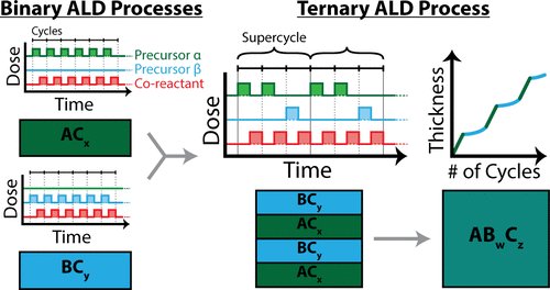
A review by Adriaan J. M. Mackus and the Bent Group at Stanford "Synthesis of Doped, Ternary, and Quaternary Materials by Atomic Layer Deposition" LINK


Picture from Twitter (https://twitter.com/ChemMater/status/1103368831337000960https://twitter.com/ChemMater/status/1103368831337000960https://twitter.com/ChemMater/status/1103368831337000960https://twitter.com/ChemMater/status/1103368831337000960https://twitter.com/ChemMater/status/1103368831337hts://twitter.com/ChemMater/status/1103368831337000960)

Applied Materials - Moore’s Law and the Shift from Near-Memory to In-Memory Compute

Beyond Von Neumann: Moore’s Law and the Shift from Near-Memory to In-Memory Compute
by David Thompson
Feb 27, 2019

In reflecting a little bit on my last blog, it probably would have been good to do a little bit of explaining around what Von Neumann computing is, before discussing what’s beyond it. However, a bit of background on Moore’s Law is in order first.


Tuesday, March 5, 2019

Welcome to Berlin for the biggest ALD Exhibition in Germany since ALD2012 in Dresden!

Welcome to Berlin for the biggest ALD Exhibition in Germany since ALD2012 in Dresden!

ALD for Industry – 3rd Workshop and Tutorial, 19-20 March 2018 in Berlin LINK

A topical workshop with focus on industrialization and commercialization of ALD for current and emerging markets

Atomic Layer Deposition (ALD) is used to deposit ultraconformal thin films with sub-nm film thickness control. The method is unique in the sense that it employs sequential self-limiting surface reactions for growth in the monolayer thickness regime. Today, ALD is a key technology in leading edge semiconductor technology and the field of application in other leading-edge industries is increasing rapidly. According to market estimates the equipment market alone is currently at an annual revenue of US$ 1.5-1.7 billion (2017) and it is expected to double in the next 4-5 years.

In a European context ALD was invented independently twice in Europe (Russia & Finland) and since the last 15 years Germany has grown to become one of the strongest European markets for ALD in R&D, chemicals, equipment and end users.

The Event will focus on the current markets for ALD and addresses the applications in semiconductor industry, MEMS & Sensors, Battery Technology, Medical, Display, Lightning, Barriers and Photovoltaics.

Friday, March 1, 2019

The hardest, thinnest, most wear-resistant coatings yet by PEALD titanium and vanadium nitrides

[Lehigh University, Story by Christine Fennessy, shortened] In August 2018, the National Science Foundation (NSF) granted Strandwitz, an assistant professor of materials science and engineering, and Krick, an assistant professor of mechanical engineering and mechanics, a Grant Opportunities for Academic Liaison with Industry (GOALI) award to work with an industry partner to study what exactly makes these nitride films so good.

Low temps, conformality, and precision yield a diamond-like toughness

Titanium and vanadium nitride films are already known to be extremely hard and wear resistant. Traditionally, they’re grown by sputtering, pulsed laser deposition, or chemical vapor deposition methods. In a first, the group’s collaborators at Veeco/CNT grew their nitride films using plasma-enhanced atomic layer deposition, or PE-ALD. Veeco/CNT is a leading supplier of ALD systems based in Waltham, Massachusetts. 

 
“In atomic layer deposition, you’re building one layer of atoms at a time,” says Strandwitz. “It’s a technique that’s already used in microelectronics, like on those in your phone, where you might need a film that is exactly three nanometers thick. If the film is four, or two, nanometers thick, your transistor switch won’t work. And you have a few billion transistors in your phone.”
 
Source: Lehigh University (LINK