Wednesday, September 19, 2018

SAVE the DATE for the 2019 CMC Conference April 25-26 in Malta/Albany, New York

SAVE the DATE for the 2019 CMC Conference, scheduled for April 25-26 in the Malta/Albany, New York area. Driven by the needs of the Critical Materials Council of semiconductor fabricators and associates (CMC), after three successful years, the CMC Conference is proven as one of the best forums for discussing actionable information relating to semiconductor fab materials. 
 

The CMC Conference is where business meets technology. Find out which materials markets are growing fastest, the drivers behind those materials and which are being constrained or limited by local or international supply-chains.
Click here to submit an abstract or get more information.

Interested in SPONSORSHIP, please contact Meena Sher by clicking here: Sponsorship Info Request

For an example agenda, from 2018, please click here.

Tuesday, September 18, 2018

IITC-MAM2019 First Call for Papers

The 22nd edition of the International Interconnect Technology Conference (IITC) is sponsored by the IEEE Electron Devices Society as the premier conference for interconnect technology. The 28th edition of the Materials for Advanced Metallization workshop (MAM) is devoted to research on materials properties and interactions of interconnect and silicide materials. These two conferences will be combined again in 2019 for the 3rd joint IITC-MAM conference and feature compelling invited talks and be proceeded by a materials workshop. 
 

Authors are encouraged to submit their original work describing innovative research and development in the critically important felid of on-chip interconnects. The conference seeks papers on all aspects of BEOL/MOL interconnects and metallization, including design, unit process, integration and reliability.

APPLICATION OF INTEREST

  • Advanced interconnects with low-k dielectrics
  • Beyond Cu interconnect, optical, wireless, and carbon
  • Contacts to MOS devices: Silicide, III-V, 2D materials
  • BEOL elements for Memory: 3D NAND, CBRAM, PCRAM, ReRAM, MRAM, DRAM
  • Advanced packaging and 3D/2.5D integration: WtW/CtW bonding, Interposer, TSV, CPI, Fan-Out techniques, Integrated Fan-Out
  • Smart technologies for interconnects: AI/neuromorphic, machine learning, big data.
TOPICS OF INTEREST
  • Process integration, advanced patterning for MOL/BEOL
  • Materials and Unit Processes: dielectrics, metals, barriers, wet, CMP, PVD, CVD, ALD, selective deposition/SAMs
  • Reliability and Failure analysis, techniques and methods
  • Advanced characterization: material analysis, analytical techniques, process modelling, defectivity, EPE
  • System scaling: design-technology co-optimization, embedded functionalities (memory, MEMS, Sensors...) Novel Systems/form factors: flexible, wearables, etc.
More information: LINK

Monday, September 17, 2018

Podcast - Introduction to ALD

In this episode me and Nicola (he is finally back) are introducing and discussing Atomic Layer Deposition, its use in the industry as well as a comparison with other technologies.

This introduction episode is the start of a multi episode series about ALD with serval experts from academia and industry. The different experts will delve deeper in several sides of the technology to cover it as much as possible.

The BALD Engineering Blog-Mobil : Sweden-Germany Roadtrip

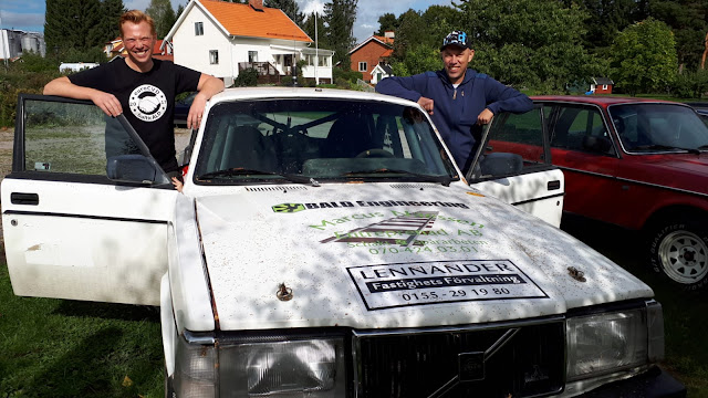
You may or may not wonder what company car BALD Engineering AB is using for covering the latest news and events in ALD technology. Until recently it was the free access to a rather embarassing 1.2 L Ford Fusion that did not really fit to the image of the company or the ALD News Blog. That is why BALD Engineering has acquired a real car - a 1988 Volvo 244 DL from one of the co-drivers from the Swedish Volvo Race Team Hjulbusarna Motorsport, which BALD Engineering is sponsoring. Below you find some nice pictures from the recent Road trip Sweden-Germany and more will follow.

OKQ8 Linköping, Sweden: The first time filling up the tank after a 400 km cruise on the Swedish Autobahn resulting in a modest 11 L/100 km fuel consumption. This gas station was very close to the Aircraft museum where the conference dinner for EuroCVD/Baltic ALD 2017 was held. Further south when hitting the German Autobahn the fuel consumption naturally went up to 12-13 L/100 km.
Oxelösund, Sweden: The very proud previous owner and co-driver at Hjulbusarna Motorsport, Stefan Gustafsson handing over his beautiful, well maintained and powerful Volvo for new adventures.

Hjulbusarna Racing Head Quarter, Stigtomata, Sweden: Meeting up with EuroCVD/Baltic ALD Chair Prof. Pedersen who scouted the Red Volvo and who is also co-driver at Hjulbusarna Motorsport.

Prof. Pedersens Garage, Stigtomata, Sweden: Decorated with the BALD Engineering Logo.
Prof. Pedersens Garage, Stigtomata, Sweden: Detailed source inspection headed by one of the junior engineers and a team of little helpers.
BALD Engineering Headqaurter, Kopparmora, Sweden: Proud owner posing with the new company car.
Gedser, Denmark: lining up for the ferry to Germany


Veeco GEN10 Automated MBE Cluster System Wins Max Planck Institute Tender, Supporting Research of Oxide-Nitride Layer Structures

Prestigious Research Institute Cited Veeco’s Expertise in MBE and the High Reliability and Customization of the GEN10™ as Key Factors in its Decision

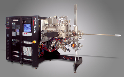
[Veeco, LINK] PLAINVIEW, N.Y., August 14, 2018—Veeco Instruments Inc. (NASDAQ: VECO) today announced that a dual chamber GEN10™ automated molecular beam epitaxy (MBE) cluster system won the tender offer by the Max Planck Institute of Microstructure Physics, Halle (Saale), Germany (MPI-MSP) to support world-class research on complex oxides. Demand for oxide-nitride layer structures has increased due to their enormous potential in enabling next-generation energy-efficient nano-devices and advanced data storage. The department of Nano-systems from Ions, Spins and Electrons (NISE) at the MPI-MSP will leverage Veeco’s MBE technology to expand research and develop innovative applications. 

Veeco's GENxplor R&D MBE System (Veeco.com)
“Our team is highly interested in exploring the properties of atomically engineered oxide-nitride layer structures especially because of their extraordinary properties but also for their potential in paving the way to novel energy-efficient nano-devices,” said Stuart Parkin, Director of the NISE Department at the MPI-MSP and Alexander von Humboldt Professor, Martin Luther University Halle-Wittenberg, Halle. “Veeco’s reputation and expertise in MBE combined with the GEN10’s high reliability, throughput, customization and automation capabilities will help support our research into novel materials.”

This win at MPI marks the first time Veeco has provided a fully integrated solution for a concentrated ozone source. The GEN10 allows for up to three configurable, material-specific growth modules, enabling high system utilization and allowing multiple researchers use the system at the same time to perform unattended growth. By expanding its reach in the R&D sector worldwide, Veeco is leading the way in helping grow complex oxide structures.

“As our MBE systems continue to expand their footprint in the global R&D space, we are honored that Veeco’s GEN10 MBE system was selected by the highly respected Max Planck Institute of Microstructure Physics in Halle,” noted Gerry Blumenstock, vice president and general manager of MBE and ALD products at Veeco. “We are pleased with the confidence Dr. Parkin and his team placed in our MBE expertise and we look forward to supporting the MPI-MSP as it continues to lead R&D exploration and applications for complex oxides.”

Wednesday, September 12, 2018

Thermal Atomic Layer Etching of copper by University of Illinois at Urbana-Champaign

Copper is a wonder metal used in moth integrated circuits but is very difficult to etch by a dry process. That is why copper is typically removed by wet chemistry or rather brutal CMP processes. So now quite fantastic news for all BEOL people who have had all kinds of problem etching copper or for those FEOL people who absolutely do not like copper - now there is a way to thermally etch copper as presented in the publication below by scientists form University of Illinois at Urbana-Champaign in the United States.

Thank you Prof. Pedersen for sharing this article on Twitter using the hashtag #ALEtch (#ALDep for ALD).

According to the abstract, the published ALE method of copper relies on:
  • a cyclic exposure to an oxidant and hexafluoroacetylacetone (Hhfac) at 275°C
  • exposure of a copper surface to molecular oxygen, O2, a weak oxidant, forms a ∼0.3 nm thick layer of Cu2O, which is removed in a subsequent step by exposure to Hhfac. 
  • the process has high selectivity and does not attack dielectrics such as SiO2 or SiNx 
  • the surface reactions are self-limiting
  • the roughness of the copper surface increases slowly over successive etch cycles 
Promising is also that rhermochemical and bulk etching data indicate that the approach should also work for other metals.

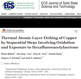
Thermal Atomic Layer Etching of Copper by Sequential Steps Involving Oxidation and Exposure to Hexafluoroacetylacetone

doi: 10.1149/2.0211809jss ECS J. Solid State Sci. Technol. 2018 volume 7, issue 9, P491-P495

Screendump from ECS Journal of Solid State Science and Technology (http://jss.ecsdl.org/content/7/9/P491.abstract?etoc 2018.12.09)

Sunday, September 9, 2018

Research breakthrough reduces cost of solar cell production by 10%

PV Magazine reports that [LINK] Researchers from Finland’s Aalto University and the Michigan Technological University, in the US, say they have demonstrated the cost per unit of power of black-Si PERC cells could fall 10.8%, despite an increase in cell processing cost. A new study in Energies*, conducted by scientists from Finland’s Alto University and the U.S.-based Michigan Technological University, however, intends to show production costs for black-Si PERC cells may be reduced by around 10% even using dry-etching, a process for making solar cells more efficient at capturing light.

Detailed manufacturing steps for texturized Czochralski PERC cells (left) and multicrystalline black-Si PERC cells (right). The overall processes are divided into wafer production (Steps 1 to 3) and cell processing (Steps 4 to 14). Their cost represent 85% and 15% of the total costs for the texturized Czochralski and 82% and 18% for the multicrystalline black-Si PERC, respectively. The steps highlighted in blue differ for the two cell architectures and are considered in the cost calculations. (Figure from the Energies Article released under Creative Commons Licence CC BY 4.0*)

According to the study in Energies above, ALD is used for the surface passivation steps and show yet another potential cost saving, since the black mc-Si PERC can effectively be passivated with a double-side ALD step prior to capping the rear side by SiNx, leading to both lower process costs and a lower number of necessary processing tools. The cost for the surface passivation by double-sided ALD is <50% of the cost for the corresponding steps by PECVD and CVD for the standard Cz process, which also includes an additional back surface polishingstep. 


Sum of the normalized costs for the PERC process steps that are different between the reference (standard texturized Cz-Si PERC) and the black mc-Si PERC. Step costs are normalized over the total steps costs for the reference device. The numbers on the black mc-Si PERC show the multiplying factor for each step in the process compared to the reference for the given process step. (Figure from the Energies Article released under Creative Commons Licence CC BY 4.0*)

However the study concludes that the largest challenge to escape the valley of death is the capital costs associated with PV industry-scaled RIE and ALD tools, which are both on the order of several million USD for a 1 GW PV plant. Therefore study recommend that governments can utilize to effectively assist industry in this respect by providing business incentive policies.


Scanning electron microscope image of reactive ion etched (RIE) black silicon [Wikipedia].

*Economic advantages of dry-etched black silicon in passivated emitter rear cell (PERC) photovoltaic manufacturing. Energies.
Modanese, C., Laine, H. S., Pasanen, T. P., Savin, H., & Pearce, J. M. (2018).
Retrieved from: https://digitalcommons.mtu.edu/materials_fp/174

Saturday, September 8, 2018

Thermal ALE of silica and alumina using TMA with Hydrogen Fluoride or Fluoroform

Hydrofluoric acid (HF) is the Achilles heel of thermal ALE of silicon and metal oxides. It is dangerous stuff to work with and if the HF it self will not kill you the yearly safety updates will. It is not that uplifting to sit and watch pictures of HF accidents - I tell you! Besides that to handle liquid HF  your ALE pimped ALD reactor will mean that you have to passivate all lines with HF prior to operation or alternatively rebuild the system using nickel valves and tubes instead.
 
So for anyone that has been through the procedure to use HF outside the regular chemical labs and are eager to get going with thermal ALE of oxides this should come as promising news. You can actually possibly skip HF and get on with the more reasonable friend fluoroform (CHF3) by using an additional water pulse that removes the fluorinated passivation. Or at least so it seems - Check it out!
 
So now we all wonder if CHF3 can be swapped for NF3...

Thermal Atomic Layer Etching of Silica and Alumina Thin Films Using Trimethylaluminum with Hydrogen Fluoride or Fluoroform
Rezwanur Rahman, Eric C. Mattson, Joseph P. Klesko, Aaron Dangerfield, Sandrine Rivillon-Amy, David C. Smith, Dennis Hausmann, and Yves J. Chabal

ACS Appl. Mater. Interfaces, Article ASAP DOI: 10.1021/acsami.8b10899
https://pubs.acs.org/doi/10.1021/acsami.8b10899
 
 
Reprinted with permission from (ACS Appl. Mater. Interfaces, Article ASAP DOI: 10.1021/acsami.8b10899) Copyright (2018) American Chemical Society.
 
Thermal atomic layer etching (ALE) is an emerging technique that involves the sequential removal of monolayers of a film by alternating self-limiting reactions, some of which generate volatile products. Although traditional ALE processes rely on the use of plasma, several thermal ALE processes have recently been developed using hydrogen fluoride (HF) with precursors such as trimethylaluminum (TMA) or tin acetylacetonate. While HF is currently the most effective reagent for ALE, its potential hazards and corrosive nature have motivated searches for alternative chemicals. Herein, we investigate the feasibility of using fluoroform (CHF3) with TMA for the thermal ALE of SiO2 and Al2O3 surfaces and compare it to the established TMA/HF process. A fundamental mechanistic understanding is derived by combining in situ Fourier transform infrared spectroscopy, ex situ X-ray photoemission spectroscopy, ex situ low-energy ion scattering, and ex situ spectroscopic ellipsometry. Specifically, we determine the role of TMA, the dependence of the etch rate on precursor gas pressure, and the formation of a residual fluoride layer. Although CHF3 reacts with TMA-treated oxide surfaces, etching is hindered by the concurrent deposition of a fluorine-containing layer, which makes it unfavorable for etching. Moreover, since fluorine contamination can be deleterious to device performance and its presence in thin films is an inherent problem for established ALE processes using HF, we present a novel method to remove the residual fluorine accumulated during the ALE process by exposure to water vapor. XPS analysis herein reveals that an Al2O3 film etched using TMA/HF at 325 °C contains 25.4 at. % fluorine in the surface region. In situ exposure of this film to water vapor at 325 °C results in ∼90% removal of the fluorine. This simple approach for fluorine removal can easily be applied to ALE-treated films to mitigate contamination and retain surface stoichiometry.

Veeco present ALD coating that reduces failure in orthopedic implants

At the EFDS ALD For Industry Workshop in Dresden this spring Ganesh Sundaram Veeco presented on their recent developments employing ALD in Life Sciences [LINK]. One of the topics presented in hos presentation was how an ALD coating can reduce failure in orthopedic implants. Here is a recent article describing these studies in details that is well worth reading along with the scientific publications.

Typical titanium implant (Wikipedia) in Osteosynthesis, which is the operative treatment of bone fractures, mainly with metal nails, plates and screws.

Atomic Layer Deposition Coating Reduces Failure in Orthopedic Implants

Written by Luting Liu, Ritwik Bhatia, Thomas J. Webster
Novus Light Technologies Today

LINK: https://www.novuslight.com/atomic-layer-deposition-coating-reduces-failure-in-orthopedic-implants_N8392.html

Introduction:

Titanium (Ti) and its alloys have been extensively used as implant materials in orthopedic applications. However, implants may fail due to a lack of osseointegration and/or infection. Researchers endowed an implant surface with favorable biological properties by the dual modification of surface chemistry and nanostructured topography. The application of a nanostructured titanium dioxide (TiO2) coating on Ti-based implants is proposed to enhance tissue-implant interactions while inhibiting bacterial colonization simultaneously due to its chemical stability, biocompatibility, and antimicrobial properties.

Temperature-controlled atomic layer deposition (ALD) was found to provide an effective strategy to produce TiO2 coatings with delicate control of surface nano-topography and surface energy to enhance the interfacial biocompatibility and mitigate bacterial infection.


Ganesh Sundaram Veeco presenting recent developments employing ALD in Life Sciences at EFDS ALD For Industry in Dresden 2018 (Photo Dr. Martin Knaut).

Original publication [Open access]: Atomic layer deposition of nano-TiO2 thin films with enhanced biocompatibility and antimicrobial activity for orthopedic implants, Liu L, Bhatia R, Webster TJ, International journal of nanomedicine 8 December 2017 Volume 2017:12 Pages 8711—8723 DOI https://doi.org/10.2147/IJN.S148065

Combining Focused Ion Beam Patterning and Atomic Layer Deposition for Nanofabrication


While the big guys are banging there heads against the wall to achieve smaller critical dimensions for Logic and Memory fabrication using classical top down Litho-Etch patterning ALD has stepped in multiple times to save the world. Some examples in high volume manufacturing:
  • ASD - Area selective deposition by ether CVD or ALD
  • SADP - Self-aligned double patterning
  • SAQP - Self-alignes quadruple patterning
  • Depositing hardmask materials and liners in advanced patterning schemes for high aspect ratio and dense features
Besides ALD, ALE is used for trimming of pattern features such as FinFETs and hardmasks, or to fabricate smallest feature nano-imprint stamps and even to split nano wires longitudinal. There is basically no end to what you can do once you have atomic level control of things.

Focused Ion Beam (FIB) is a technology that is available in most material analytical labs and fabs as in-line metrology to make sample preparations or repair and is also used in standard manufacturing for lithography masks, i.e., there are tools out there that can shuffle substrates and 300 mm wafers at high speed.

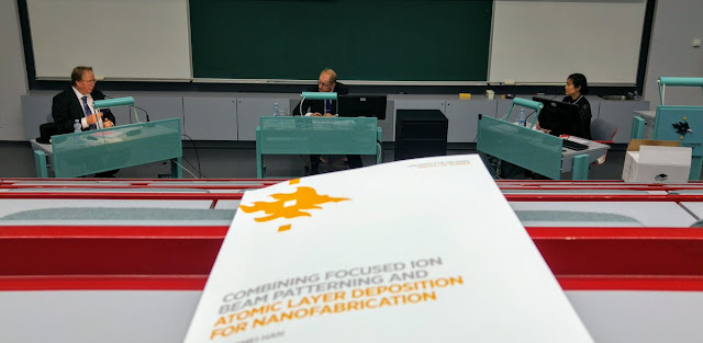
Ph.D. Thesis defence (picture from Twitter, HelsinkiALD

That is why this thesis by Zhongmei Han is indeed very interesting and worth reading - congratulations to the recent defense in Helsinki!

Combining Focused Ion Beam Patterning and Atomic Layer Deposition for Nanofabrication

Doctoral Thesis, Zhongmei Han
Department of Chemistry, Faculty of Science, University of Helsinki, Finland

For nanofabrication of silicon based structures, focused ion beam (FIB) milling is a top-down approach mainly used for prototyping sub-micron devices, while atomic layer deposition (ALD) is a bottom-up approach for depositing functional thin films with excellent conformality and a nanometer level accuracy in controlling film thicknesses. Combining the strengths of FIB milling with ALD provides new opportunities for making 3D nanostructures. In FIB milled silicon, the gallium implanted surface suffers from segregation and roughening upon heating, which makes the thermal stability of the as-milled substrate a concern for the following ALD processes which are typically performed at temperatures of 150 ℃ and higher. This study aimed to explore methods for improving the thermal stability of FIB milled silicon structures for the following ALD processes. The other aim was to fabricate nanostructures by alternately using FIB milling and ALD approaches on silicon and oxide thin film materials. The experiments were started on the reduction of gallium implantation during FIB milling of silicon substrates using different incident angles. Oblique incidence of the ion beam was found an effective method for improving the thermal stability of the FIB milled silicon surfaces by decreasing their gallium content. The improved thermal stability allowed to apply ALD Al2O3 on the FIB milled surfaces to make nanotrenches. Wet etching in KOH/H2O2 was found as a second method for improving the thermal stability by removing the gallium implanted silicon layer. ALD Al2O3 thin films can be applied as milling masks to limit amorphization of silicon upon FIB milling. With the aid of KOH/H2O2 etching, nanopore arrays, nanotrenches and nanochannels were fabricated. ALD grown Al2O3/Ta2O5/Al2O3 multilayers were FIB milled and wet etched to form both 2D and 3D hard masks. The fabricated 2D masks were used for making metal structures which are applicable for electrical connections. Thin film resistors were also fabricated using this 2D mask system. In conclusion, this study illustrates that combining FIB patterning and ALD is feasible for 3D nanofabrication when the stability of FIB milled surfaces is considered and improved. 
 

Thursday, September 6, 2018

Atomic Layer Etching: Rethinking the Art of Etch

Yet another Must Read ALE journal publication from Lam Reaserach Keren Kanarik and team. Please enyoy!

Atomic Layer Etching: Rethinking the Art of Etch

Keren J. Kanarik, Samantha Tan, and Richard A. Gottscho
The Journal of Physical Chemistry Letters 2018 9 (16), 4814-4821
DOI: 10.1021/acs.jpclett.8b0099
 
 
Atomic layer etching (ALE) is the most advanced etching technique in production today. In this Perspective, we describe ALE in comparison to long-standing conventional etching techniques, relating it to the underlying principles behind the ancient art of etching. Once considered too slow, we show how leveraging plasma has made ALE a thousand times faster than earlier approaches. While Si is the case study ALE material, prospects are better for strongly bound materials such as C, Ta, W, and Ru. Among the ALE advantages discussed, we introduce an ALE benefit with potentially broad application—the ALE smoothing effect—in which the surface flattens. Finally, regarding its well-established counterpart of atomic layer deposition (ALD), we discuss the combination of ALE and ALD in tackling real world challenges at sub-10 nm technology nodes


Wednesday, September 5, 2018

Arbeitskreistreffen ALD Lab Saxony & ALD Fest 2018

Am 12. September 2018 findet das nächste Treffen des "ALD Lab Saxony", dem Interessenverbund für Atomic Layer Depositon unter dem Dach des Cool Silicon e. V., statt. Hierzu laden wir alle Cool Silicon Mitglieder sowie Interessierte ein.


Weiterführende Informationen finden Sie : https://www.cool-silicon.de/termine/termin-detail/?tx_na5108easyevent_na5108easyevent%5Bna5108easyevent%5D=410

Sponsoring:


Veeco Announces Changes to Executive Leadership Team

PLAINVIEW, N.Y., September 4, 2018 —Veeco Instruments Inc. (NASDAQ: VECO) today announced that John Peeler, Chairman and Chief Executive Officer, will transition to the role of Executive Chairman, effective October 1, 2018. William J. Miller, currently President, will become Chief Executive Officer and will join the Company’s board of directors bringing the size of the board to eight. Additionally, Shubham (Sam) Maheshwari will be named Chief Operating Officer and will continue in his role as Chief Financial Officer. 

Peeler joined Veeco in 2007 as Chief Executive Officer and became Chairman of the Board in 2012. As Executive Chairman, Peeler will work closely with Miller and the Board to ensure an effective transition of management.

“With his impressive background and track record of notable achievements across strategic, product development and operational assignments, there is no one better suited than Bill to take over the helm as Veeco looks forward to its next chapter,” stated Peeler. “Bill and the executive team have the industry experience to execute Veeco’s vision while remaining committed to enabling tomorrow’s technology breakthroughs.”

Tuesday, September 4, 2018

Postdoctoral Associate / Young Investigator (m/f/d) Atomic Layer Deposition / Etching for Functional Nanostructured Materials

The Leibniz Institute for Solid State and Materials Research Dresden – in short IFW Dresden – is a non-university research institute and a member of the Leibniz Association. The IFW employs approximately 600 people and one focus is on the training of young scientists besides enhancing fundamental and applied research development. At the highest international level, the IFW operates modern materials science on a scientific basis and makes the obtained results useful for the economy. The complex and interdisciplinary research work is carried out within the IFW by five scientific institutes, which are sup-ported by a highly developed technical infrastructure. The IFW supports its employees in reconciling work and family life and regularly submits to the berufundfamilie® audit.

Further information at: http://www.ifw-dresden.de

Postdoctoral Associate / Young Investigator (m/f/d)

Atomic Layer Deposition / Etching for Functional Nanostructured Materials

We are searching for a young investigator at the Institute for Metallic Materials (IMW) at the IFW Dresden focusing on the application of atomic layer deposition/etching (ALD/ALE) for the development of novel nanostructured materials and their device applications. In the future she or he should give significant contributions at least to one of the following research activities by engaging the recently established ALD laboratories e.g.: (a) layered/quantum materials and devices (b) thermoelectric materials or (c) magnetic and ferroic materials (nanograined bulk and thin films).

Saturday, September 1, 2018

PEALD - Alumina Systems & Plasway Technologies rewarded "Best Component Award" at CERAMITEC 2018

Alumina Systems GmbH was awarded the "Best Component Award" for its development of a ceramic gas distributor ring. For the first time this year, the prize was awarded by the trade magazine "Ceramic Applications". At the CERAMITEC 2018 trade fair in Munich.


The award-winning component is a ceramic distribution ring for PEALD (Plasma Enhanced Atomic Layer Deposition) processes. The aluminum oxide ring has a diameter of 380 mm and consists of three horizontally divided rings, which are joined with glass solder. In addition, 3-D printed ceramic nozzles made of 99.99% Al2O3 have been soldered in at the same time for internal gas distribution. The ring can supply 2 gases (precursors) at the same time or sequentially into a 300 mm PEALD chamber.


The managing director of Alumina Systems GmbH, Dr. med. Holger Wampers (left) and development partner and customer Stephan Wege, managing director of Plasway Technologies GmbH.

To make it even more complicated, the gas connection for the precursors is made by a titanium tube, which is then soldered to two 3D-printed stainless steel tubes. Both metal solderings are attached via a downstream active soldering. All joining operations are cascaded in the temperature control, i. the process with the highest temperature must first be carried out, further processes must always be lower in temperature so that previous solder joints do not break up again. Besides from the metal parts, the components and joining processes were manufactured or carried out at Alumina Systems in Redwitz. "We have used all our know-how in this component," emphasized Dr. med. Wampers and added: "The horizontally split rings must be in relatively close tolerances for flatness and roundness after sintering, otherwise this can not be corrected with the subsequent grinding process for technological reasons. This is not so easy to achieve due to the shrinkage process of around 20%. Another challenge was the Laval nozzles, which could not have been produced without a 3-D printer. In addition, the entire ring is He leak-tight to 10-8 mbar · L / s "


For more details you can browse the current issue of Ceramic Applications 2/2018 : LINK
As well as Plasway Technologies GmbH (LINK), Fraunhofer IKTS Thin Film Technology Group (LINK) and Alumina Systems news: LINK (German)

Updated website NCD for ALD technology and equipment


Updated website NCD for ALD technology and equipment: www.ncdtech.co.kr

NCD updated its website with re-formation and the new company promotional video clip for the introduction and main equipment.


Announcing Kronos™ 1080 and ICOS™ F160 Inspection Systems: Expanding KLA-Tencor's IC Packaging Portfolio

KLA-Tencor has announced it is expanding its integrated circuit (IC) packaging portfolio with two new defect inspection products designed to address a wide variety of IC packaging challenges: KronosTM 1080 and ICOS™ F160. The two new inspection systems join KLA-Tencor’s portfolio of defect inspection, metrology and data analysis systems that help accelerate packaging yield and increase die sort accuracy. You may find the official release here;

Highlights: 
  • Kronos 1080 – offers production-worthy, high sensitivity wafer inspection for advanced packaging, providing key information for process control and material disposition.
  • ICOS F160 – examines packages after wafers have been diced, delivering fast, accurate die sort based on detection of key defect types—including sidewall cracks, a new defect type affecting the yield of high-end packages. 
 Kronos™ 1080 and ICOS™ F160 (Image shared by KLA-Tencor)

Thursday, August 30, 2018

How to split nanowires by Atomic Layer Etching

The master thesis by Sabbir A. Khan based on work completed at Lund Nano Lab, Lund University Sweden, has finally been released from secrecy [Patent application WO2017157902A1]. Please find below the abstract and link to the full version. Sabbir is now a Ph.D. candidate in Quantum Materials at Microsoft Quantum Materials Lab (MQML) and Center for Quantum Devices, Niels Bohr Institute, University of Copenhagen, Denmark. There his research focuses on as-grown epitaxial nanowire based networks for scalable quantum computation. The main goal is to develop innovative fabrication techniques that can realize new device concepts based on as-grown nanowire networks.
 

Evaluation of Atomic Layer Etching Possibility at Lund Nano Lab [LINK PDF]
Next you will have a chance to meet Sabbir at the PSE 2018 Tutorial, Plasma assisted atomic level processing – PEALD & ALE Sunday, September 16, 2018 in Garmisch-Partenkirchen, Germany.
Abstract
In modern electronics, device downscaling demands atomic precision control and Atomic Layer Etching (ALE) can provide this prime capability with minute device damage. ALE, also known as layer-by-layer etching, is a technique of removing atomically thin layers from the surface of materials in a controlled way. This technique is now very crucial for nanofabrication and semiconductor industry in order to achieve atomic scale resolution. This is why the overall goal of this diploma project was to investigate the possibility for ALE at Lund Nano Lab and to reveal different limitations with our current equipment. In order to achieve this goal we have done experiments with conventional system used for reactive ion etching. In addition, the ALE has been done on GaP nanowires and on Si surface patterned with high-resolution Electron Beam Lithography (EBL). The results of these experiments indicate that the process can be used to make stamps for nanoimprint lithography in a highly controlled way and that the low ion energy etching process can be used for direct nanowire splitting. We show different limitations for ALE with our current equipment and provide recommendations for new equipment dedicated for this process. In this way, the work presented here opens up the possibility for further studies of ALE with conventional equipment, shows some aspects of it’s importance for nanofabrication and suggests new applications for the ALE processes.
Popular Abstract
Nowadays electronic devices are getting smaller and much more efficient. However, it’s getting much harder to fabricate such small devices. Specifically, device fabrication with feature sizes below 10 nm (a human hair is 100,00 nm wide) is a big challenge. For this, atomic level control is needed. Atomic layer etching (ALE) is one of the key technologies that can provide atomic controlled etching of different materials by a cyclic etching, where an (sub) atomically thick layer is etched in every cycle. There are also other technologies, which have a potential for the sub 10 nm fabrication. For instance nanoimprint lithography, which is alike book printing but for extremely small features in nanometer range, and epitaxial semiconductor nanowires grown from seed catalytic particles by different epitaxial techniques have a very big potential for extremely fine fabrication of nanostructures. These techniques are also very active research areas in Lund and have already enabled many important applications. This is why the combination of ALE with these techniques may open up many new interesting opportunities. For example, the nanoimprint lithography can be only as good as the stamps, which are used for the nanoimprint, and ALE may provide a very good mean of the stamp fabrication with subatomic precision.

Sabbir A. Khan splitting Nanowires at Lund Nanolab using the Oford Instruments Plasmalab 100 System.

Different III-V semiconductor nanowires are very important for their electrical and optical properties. Diameter of the usual nanowires lies in the 40-100 nm range and with ALE it might be potentially possible to shrink the nanowire diameter to the sub 10 nm range. In this research work we used a system for reactive ion etching, similar to the systems, which are widely used in semiconductor industry for semiconductor device fabrication, for testing ALE possibility in Lund Nano Lab. We demonstrated that with this equipment it is possible to perform ALE and used this process for etching semiconductor horizontal nanowires and to make stamps for nanoimprint lithography. Surprisingly, we found that, due to some specific properties of the ALE process and a hexagonal cross section of nanowires, which we used in our experiments, after ALE each nanowire is split in to two very thin nanowires. We believe that here the inclined nanowire surfaces act as a mask for the etch process and that potentially this technique can enable fabrication of ever smaller semiconductor devices in a controllable and industrially relevant way. For instance, a core part of every transistor is a transistor channel and we can foresee that this technique may enable splitting of the transistor channel into two channels without additional expensive and challenging lithographic steps. In this way we may enable further downscaling of transistors in a very economical and practical way by this helping further downscaling of electronic devices

Wednesday, August 29, 2018

Review and perspective on ferroelectric HfO2-based thin films for memory applications

JVSTA Call for Research Articles - Atomic Layer Deposition and Atomic Layer Etching

This special topic collection is planned in collaboration with ALD 2018 and the ALE 2018 Workshop to be held in Incheon, South Korea during July 29—August 1, 2018. The Special Topic Collection will feature sections dedicated to the science and technology of atomic layer controlled deposition and to the science and technology of controlled etching of thin films. While a significant number of articles will be based on material presented at ALD 2018 and the ALE 2018 Workshop, research articles on ALD and ALE but not presented at this conference are also welcome. The special topic collection will be open to all articles on the science and technology of ALD and ALE.

Authors are encouraged to use the JVST templates. Online, you will have an opportunity to tell us that your paper is a part of the Special Topic Collection by choosing either the “ALD Special Topic Collection” or the “ALE Special Topic Collection.”


Tuesday, August 28, 2018

Stress-free ALD High-k from Picosun

ESPOO, Finland, 28th August, 2018 – Picosun Group, a leading supplier of advanced Atomic Layer Deposition (ALD) thin film coating solutions, reports a method to control and eliminate stress in ALD films.

Various stresses are easily formed in ALD films during the deposition process, either inside the film or between the film and the underlying substrate. As all modern microelectronic devices are basically built by stacking ultra-thin layers of various materials on top of each other, these stresses can be detrimental not only to the film itself but to the other functional layers and structures beneath. Especially in MEMS devices, where cavities and free-standing membranes are often employed, stress-free ALD films, or films where the stress is exactly controlled, are very much sought after. Same applies for IC components, where film strains and tensions can lead to material layers detaching from each other, or bending and buckling of the whole structure. 
 
 
Picosun has now developed a method with which zero stress and controlled stress ALD films can be produced. This sophisticated method is based on intricate tuning of process chemistry and deposition conditions. The desired effect is obtained with right selection of precursor chemicals and process temperature, so no additional process steps such as heat or plasma treatments (which might cause structural damage to the film) are required. Replacing a single material film with carefully designed nanolaminate of materials with opposite stress properties is another way to achieve zero stress layers. These methods have been validated with e.g. HfO2, which is one of the key materials in microelectronics industry. Other ALD materials tested include SiO2, Ta2O5, and TiO2 (*). 


“We are very pleased that we can now offer stress-free ALD HfO2 process to our customers in MEMS and IC industries. Especially medical MEMS is an important market for us, and a prime example of an application area where controlled stress ALD films are needed to enable a whole platform of novel products. Thanks to our unmatched ALD expertise, we have now developed a solution to one of the fundamental challenges in ALD. This will facilitate the implementation of ALD to yet new, exciting applications in health technology and future IC manufacturing,” summarizes Dr. Jani Kivioja, CTO of Picosun Group.

Monday, August 27, 2018

The Swedish Catalysis Society presented the prize to Professor Puurunen in Copenhagen on 27 August 2018.

[Aalto School of Chemical Engineering News] The Berzelius Medal is given in the honour of the famous Swedish researcher Berzelius. The prize winner has to be aged under 45 years, female every second time and working in a Nordic country. Each country can come up with one proposal. Professor Puurunen was proposed by the Finnish Catalysis Society. 
 

Photo: Mika Huuhtanen
 
The candidate should have performed research in the field of catalysis and her/his work should have generate a new concept, idea or explanation; a new way to tackle a scientific problem; or an introduction of a new word or phrase that is significant. Candidates are evaluated by 4 international experts (2 female, 2 male) who will make an evaluation report on them.

"I feel extremely grateful and honoured to receive the Berzelius Prize. The prize is a great recognition for my persistent and on-going work to understand the details of atomic layer deposition (ALD). ALD is a technology which was awarded Millennium Technology Prize 2018 and whose importance is growing in the field of catalysis, too," says Professor Puurunen.

Professor Puurunen received the prize at the 18th Nordic Symposium on Catalysis. The event is organized every othe year and its aim is to create a breeding ground for ideas by ensuring meetings between researchers and catalyst developers, from academy as well as industry, within all aspects of catalysis.

Sunday, August 26, 2018

The Luxembourg Institute of Science and Technology (LIST) will organize the EuroCVD 22 - Baltic ALD 16 from 24 to 28 June 2019 in Luxembourg

The Luxembourg Institute of Science and Technology (LIST) will organize the EuroCVD 22 - Baltic ALD 16 from 24 to 28 June 2019 in Luxembourg. 

Chemical Vapor deposition (CVD) and Atomic Layer Deposition (ALD) are essential and versatile tools for the development of innovative materials and architectures that are the hart of modern nanotechnology. 


The conference subscribes within the biennial series of European CVD conferences, which started in Paris (1977), and the Baltic ALD series launched as Atomic Layer Epitaxy Symposium in Helsinki (1991). From the process and materials development perspectives, this conference will be a showcase of the forefront research addressing up-to-date challenges and stat-of-the-art chemical processing from the gas phase (CVD, ALD, Energy assisted CVD/ALD, MOVPE, RIE, ALE). The conference covers processes that are performed at atmospheric pressure, low vacuum and ultra-high vacuum, and processes that are assisted thermally or with other means such plasma, plasmon, light, electrical field, hot wire, … 

The EuroCVD 22 – Baltic ALD 16 will offer a high quality scientific program with invited and contributed lectures in key development areas based the chemical processing from the gas phase.
More details will be available soon.

Saturday, August 25, 2018

Tyndall National Institute present the first computational study of thermal Atomic Layer Etch of metal oxides by exposure to HF

Modeling the Chemical Mechanism of the Thermal Atomic Layer Etch of Aluminum Oxide: A Density Functional Theory Study of Reactions during HF Exposure

Suresh Kondati Natarajan and Simon D. Elliott
Tyndall National Institute, University College Cork
Chem. Mater., Article ASAP
DOI: 10.1021/acs.chemmater.8b01930, Publication Date (Web): August 9, 2018


Reprinted with permission from (DOI: 10.1021/ACS.CHEMATER.8b01930). Copyright (2018) American Chemical Society.

Thermal atomic layer etch, the reverse of atomic layer deposition, uses a cyclic sequence of plasma-free and solvent-free gas surface reactions to remove ultrathin layers of material with a high degree of control. A theoretical investigation of the hydrogen fluoride pulse in the thermal atomic layer etch of monoclinic alumina has been performed using density functional theory calculations. From experiments, it has been suggested that the HF pulse forms a stable and nonvolatile layer of AlF3 on an alumina surface. Consistent with this, the desorption of an AlF3 molecule from an HF-saturated surface was computed to be energetically unfavorable. HF molecules adsorbed on the alumina surface by forming hydrogen bonds and either remained intact or dissociated to form Al–F and O–H species. At higher coverages, a mixture of molecularly and dissociatively adsorbed HF molecules in a hydrogen-bonded network was observed. Binding energies converged as the coverage of dissociated F became saturated, consistent with a self-limiting reaction. The formation of H2O molecules in the HF pulse was found to be endoergic with an energy barrier of at least +0.9 eV, but their subsequent desorption was computed to cost as little as +0.2 eV. On the basis of a model of the saturated Al–F surface, the theoretical maximum of the etch rate was estimated to be −0.57 ± 0.02 Å/cycle (−20.0 ± 0.8 ng cm–2 cycle–1), which matches the range of maximum experimental values. The actual etch rate will, however, be dependent on the specific reagent used in the subsequent step of the atomic layer etch cycle. 


Monday, August 20, 2018

Overview of Applied Materials cobalt metallization for local interconnects

For those of you interested in the details behind the Applied Materials integrated cobalt metallization process Jonathan Bakke has written two informative blogs about it in Semiconductror Engineering:

(1) The Role Of Cobalt In Enabling AI - For continued performance, power, area and cost improvements, materials need to be engineered at the atomic scale.
(2) The Materials Side Of AI - What comes after tungsten fill for contacts and copper for the lowest-level interconnects?
The integrated cobalt solution using Applied Materials platforms (Applied Materials).

Jonathan Bakke is global product manager for Contact and Middle of Line Products in the Metal Deposition Products Business Unit at Applied Materials. He details the process flow and tool sets from Applied Materials involved in the complete BEOL Co metallization flow:

  • PVD titanium and ALD titanium nitride for the silicide and barrier layers
  • PVD cobalt serves as an anchor layer to ensure good cobalt adhesion to the bottom of the feature
  • CVD cobalt is then used to deposit a conformal film to bulk fill the feature
  • Anneal purifies and reflows the cobalt, removes the CVD seam, and merges crystal grains to form a more crystalline, lower resistance material
  • PVD cobalt for a thick overburden film
  • CMP removes overburden materials to create a smooth planar surface
  • E-beam technology monitors the process and detects voids