Registration to HERALD SUMMIT 2018 is open. The HERALD Summit will be the premier European conference in 2018
devoted solely to atomic level processing, covering atomic layer
deposition (ALD), atomic layer etch and related nano fabrication
techniques. As the final meeting of the HERALD COST Action, the
three-day Summit will include detailed discussions on the research
achievements of HERALD and on future opportunities for collaboration,
both within Europe and worldwide. Ongoing projects and new funding
proposals will be promoted so as to continue to build the ALD
community. The HERALD Summit will take place in Braga, Portugal from
25-28 September 2018.
Those receiving a travel grant from HERALD for this conference may claim reimbursement of the meals fee, but not of the registration fee (early bird registration fee € 120).
The International Iberian Nanotechnology
Laboratory (INL) is the result of a joint decision of the Governments of
Portugal and Spain, whereby the two Governments made clear their
commitment to a strong cooperation in ambitious science and technology
joint ventures for the future. INL has 47 000 m2 campus area, about 26 000 m2, providing 22 000 m2
of laboratory space and state-of-art equipment for various research
areas. A guided visit to the INL is included in the Program.
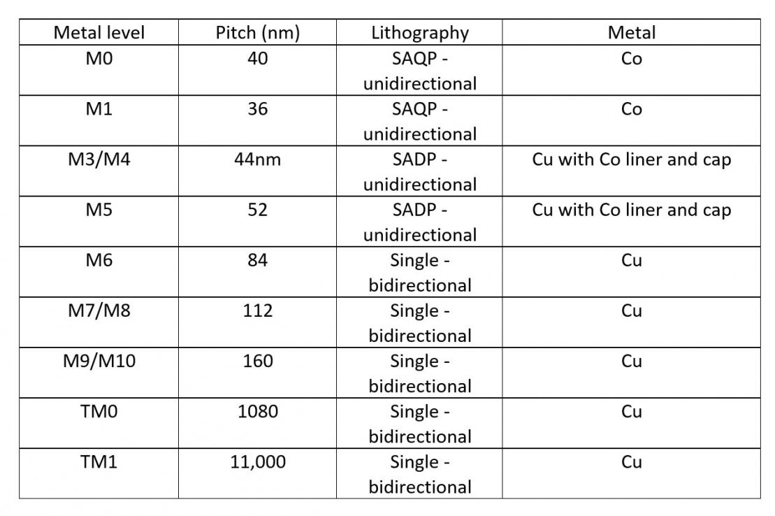
By reading this it is not possible to determine exactly how Ruthenium is used or how it has been deposited and there are several options like barrier and seed layer for plating Copper or Cobalt. What is known is that Intel presented already at IEDM2017 the use of cobalt in their 10 nm MOL/BEOL process flow as contacts and M0/M1 lines as well as barrier/seed for copper and copper cap for complete encapsulation of copper up to M5.
Intel 10nm mid end of line cobalt and copper metallization as presented at IEDM 2017.
This Special Issue is dedicated to current research activities on Materials Science
in Finland (LINK), providing a collection of outstanding contributions from diverse research groups on the recent progress regarding silicon and silica nanomaterials, DNA nanotechnology, micro/nano‐motors, biomass‐based nanostructures, nanocellulose, 2D layered materials, atomic layer deposition, superhydrophobic surfaces, and microrobots, from the University of Helsinki, Aalto University, VTT, the University of Turku, Åbo Akademi University, Tampere University of Technology, and the University of Eastern Finland
Including off course an ALD contribution from Helsinki University!
Jani Hämäläinen, Miika Mattinen, Kenichiro Mizohata, Kristoffer Meinander, Marko Vehkamäki, Jyrki Räisänen, Mikko Ritala, Markku Leskelä
First Published: 05 January 2018
Growth of rhenium disulfide by atomic layer deposition is studied. ReS2 is a 2D material that is not limited to the monolayer thickness because of effective decoupling of the monolayers in bulk. The ReS2 films are deposited from ReCl5 and H2S at up to 500 °C, also on a 3D structure, and the films are characterized.
[PV Magazine] UNSW’s Martin Green pioneering work in developing crystalline silicon solar has now gained global recognition in the energy sector – after being awarded Russia’s Global Energy Prize.
Green, the Director of the UNSW’s Australian Centre for Advanced Photovoltaics was awarded the Russian Global Energy Prize last week. He was selected by a committee of peers ahead of 44 contenders from 14 countries.
Green has long been credited as being the creator of the Passivated Emitter Rear Contact (PERC) solar cell, which continues to be adopted as a mainstream technology by manufacturers in 2018. Additionally, he has also spearheaded work into perovskites, selective emitter technology, and is now leading research into whole new areas of semiconductor material, for silicon-tandem cells that could potentially push efficiencies up to 30% and beyond.
Martin Green and fellow UNSW scientists were prominent at the recent SNEC trade show and conference in China, both progressing their work with industry partners on the advanced hydrogenation process, but also in collaborations ranging across PV cell production including Atomic Layer Deposition processes for PERC cell production.
In late April (April 29 – May 1, 2018) the 3rd Area Selective Deposition Workshop (ASD 2018), was held at North Carolina State University in Raleigh North Carolina USA (LINK). This years workshop was organized with full support from AVS and as for ALD and ALE Della Miller was in charge.
The
Workshop brought together leading international scientists and
engineers from academia and industry from all regions to share results
and insights into: 1) fundamental principles and barriers to area
selective deposition; 2) technological needs and challenges of ASD; 3)
new chemical approaches and processes to address the expanding needs;
and 4) surface characterization techniques and metrology innovation for
ASD.
This third year the program was expanded to two days, including 11 invited presentations, an invited panel discussion, 18 contributed talks, and 15 posters and in between there was plenty of time for interaction over meals and social events.
ASD2018 brought together leading experts from 10 countries in Asia, Europe and America, to deliver and discuss more than 45 presentations. As the chart shows, this constitutes significant growth since the first ASD Workshop in 2016 (ASD2018 Book of Abstracts).
As a particular focus this year, the committee had chosen to highlight the challenge of selective deposition metrology, including an invited panel to discuss particular issues and techniques related to selectivity measurement and selective defect quantification.
It is clear that ASD is a fast growing field and may at some point in time reach the status as a stand alone segment with respect to processing, chemicals and equipment. Another indication can be seen that at the SPIE in February there was a high number of presentations and posters on combining ALD and ALE or just Area Selective Deposition.
Program Char Prof. Gregory N. Parsons of North Carolina State University, USA has asked to share some photos form the successful event (below). In addition, an article covering the event was just published by Chemical & Engineering News (LINK) including interviews and the latest insights from Dennis M. Hausmann (Lam Research), Gregory N. Parsons, Silvia Armini (invited speaker, imec), Dara Bobb-Semple and Stacey F. Bent (Stanford University), and Steven M. George (Colorado Boulder University).
Studying the Book of Abstract, my personal favorite is the atmospheric pressure micro-plasma printer for area-selective ALD presented by Prof. Kessels (TU Eindhoven). This technology is being commercialized by the Dutch company with InnoPhysics (LINK) and you can expect to hear more details about this exciting technology soon.
Rear view from the The StateView Hotel conference room (Photo: Gregory N. Parsons).
Junling Lu from University of Science and Technology of China, Hefei presenting "Bottom-up Engineering Catalyst Nanostructures using Area-Selective Atomic Layer Deposition" (Photo: Gregory N. Parsons).
JVST A Featured Article: Achieving ultrahigh etching selectivity of SiO2 over Si3N4 and Si in atomic layer etching by exploiting chemistry of complex hydrofluorocarbon precursors by Kang-Yi Lin, Chen Li. Sebastian Engelmann, Eric A. Joseph, Dominik Metzler and Gottlieb Oehrlein a collaboration between University of Maryland and IBM
LEUVEN, June 4, 2018 – At this week’s 2018 IEEE International Interconnect Technology Conference (IITC 2018), imec, the world-leading research and innovation hub in nanoelectronics and digital technology, will present 11 papers on advanced interconnects, ranging from extending Cu and Co damascene metallization, all the way to evaluating new alternatives such as Ru and graphene. After careful evaluation of the resistance and reliability behavior, imec takes first steps towards extending conventional metallization into to the 3nm technology node.
For almost two decades, Cu-based dual damascene has been the workhorse industrial process flow for building reliable interconnects. But when downscaling logic device technology towards the 5nm and 3nm technology nodes, meeting resistance and reliability requirements for the tightly pitched Cu lines has become increasingly challenging. The industry is however in favor of extending the current damascene technology as long as possible, and therefore, different solutions have emerged.
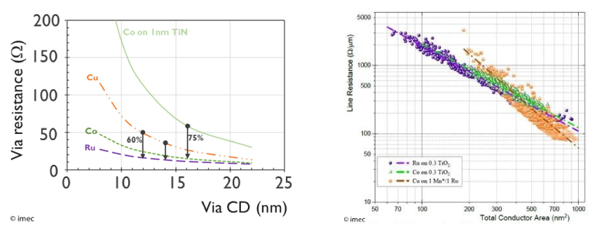
Via resistance for Co, Cu, Ru (left); and comparison of damascene
line resistance versus total conductor cross-sections area of Ru, Co and
Cu nanowires (right)
To set the limits of scaling, imec has benchmarked the resistance of Cu with respect to Co and Ru in a damascene vehicle with scaled dimensions, demonstrating that Cu still outperforms Co for wire cross sections down to 300nm2 (or linewidths of 12nm), which corresponds to the 3nm technology node. To meet reliability requirements, one option is to use Cu in combination with thin diffusion barriers such as tantalum nitride (TaN)) and liners such as Co or Ru. It was found that the TaN diffusion barrier can be scaled to below 2nm while maintaining excellent Cu diffusion barrier properties.
For Cu linewidths down to 15–12nm, imec also modeled the impact of the interconnect line-edge roughness on the system-level performance. Line-edge roughness is caused by the lithographic and patterning steps of interconnect wires, resulting in small variations in wire width and spacing. At small pitches, these can affect the Cu interconnect resistance and variability. Although there is a significant impact of line-edge roughness on the resistance distribution for short Cu wires, the effect largely averages out at the system level.
An alternative solution to extend the traditional damascene flow is replacing Cu by Co. Today Co requires a diffusion barrier – an option that recently gained industrial acceptance. A next possible step is to enable barrierless Co or at least sub-nm barrier thickness with careful interface engineering. Co has the clear advantage of having a lower resistance for smaller wire cross-secions and smaller vias. Based on electromigration and thermal storage experiments, imec presents a detailed study of the mechanisms that impact Co via reliability, showing the abscence of voids in barrierless Co vias, demonstrating a better scalability of Co towards smaller nodes. The research is performed in cooperation with imec’s key nano interconnect program partners including GlobalFoundries, Huawei, Intel, Micron, Qualcomm, Samsung, SK Hynix, SanDisk/Western Digital, Sony Semiconductor Solutions, TOSHIBA Memory and TSMC.
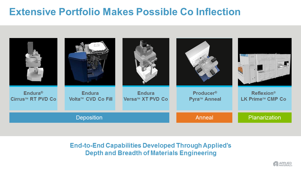
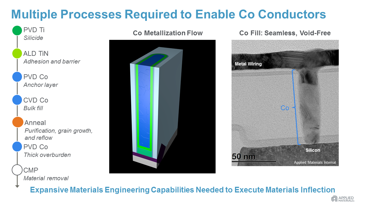
At IEDM 2017 in December both Intel and Globalfoundries presented cobalt encapsulation (liner and cap) for copper local interconnects as well as Co fill contacts for their 10nm resp 7nm technologies. Since then many have wondered about the unit process details behind the new cobalt integration and here we have it - The Applied Materials complete cobalt solution as announced yesterday. Especially interesting that TiN ALD also is used as a cobalt seed/adhesio/dufusion barrier for cobalt contacts. The most interesting stuff you will finde here: LINK
[SANTA CLARA, Calif., June 05, 2018] Applied Materials, Inc. today announced a breakthrough in materials engineering that accelerates chip performance in the big data and AI era.
In the past, classic Moore’s Law scaling of a small number of easy-to-integrate materials simultaneously improved chip performance, power and area/cost (PPAC). Today, materials such as tungsten and copper are no longer scalable beyond the 10nm foundry node because their electrical performance has reached physical limits for transistor contacts and local interconnects. This has created a major bottleneck in achieving the full performance potential of FinFET transistors. Cobalt removes this bottleneck but also requires a change in process system strategy. As the industry scales structures to extreme dimensions, the materials behave differently and must be systematically engineered at the atomic scale, often under vacuum.
To enable the use of cobalt as a new conducting material in the transistor contact and interconnect, Applied has combined several materials engineering steps – pre-clean, PVD, ALD and CVD – on the Endura® platform. Moreover, Applied has defined an integrated cobalt suite that includes anneal on the Producer® platform, planarization on the Reflexion® LK Prime CMP platform and e-beam inspection on the PROVision™ platform. Customers can use this proven, Integrated Materials Solution to speed time-to-market and increase chip performance at the 7nm foundry node and beyond.
“Five years ago, Applied anticipated an inflection in the transistor contact and interconnect, and we began developing an alternative materials solution that could take us beyond the 10nm node,” said Dr. Prabu Raja, senior vice president of Applied’s Semiconductor Products Group. “Applied brought together its experts in chemistry, physics, engineering and data science to explore the broad portfolio of Applied’s technologies and create a breakthrough Integrated Materials Solution for the industry. As we enter the big data and AI era, there will be more of these inflections, and we are excited to be having earlier and deeper collaborations with our customers to accelerate their roadmaps and enable devices we never dreamed possible.”
While challenging to integrate, cobalt brings significant benefits to chips and chip making: lower resistance and variability at small dimensions; improved gapfill at very fine dimensions; and improved reliability. Applied’s integrated cobalt suite is now shipping to foundry/logic customers worldwide.
Applied Materials, Inc. (Nasdaq:AMAT) is the leader in materials engineering solutions used to produce virtually every new chip and advanced display in the world. Our expertise in modifying materials at atomic levels and on an industrial scale enables customers to transform possibilities into reality. At Applied Materials, our innovations make possible the technology shaping the future. Learn more at www.appliedmaterials.com.
Today we at the Thin Film Technology group of Fraunhofer IKTS in Dresden were honored to be the 2nd stop for the delegation from the
ShenZhen Association for Vacuum Technology Industries from China on
their European Trip. We presented the latest research and
industrialization of Atomic Layer Deposition technology and discussed new opportunities for ALD industrial application.
Shenzhen is one of the most dynamic cities in China. It is located in
the southern part of Guangdong Province, next to Hong Kong. Shenzhen is famous for its rapid economic development since the
establishment of the special economic zone in 1980. Over the past
several decades, Shenzhen has been developed from a small fishing
village to currently a modern city featured for innovation and
high-tech. Many renowned high-tech companies such as Huawei, Tencent,
and BYD are located in Shenzhen.
The next China ALD Confernce will be held in Shenzhen, China, from October 14 to 17, 2018 (LINK)
PERC technology developed by TU Eindhoven and others has become the new standard for mono crystalline solar cells. One of the key process modules is the back side passivation with Al2O3, which is either deposited by PECVD or ALD followed by a SiN capping. According to a recent report by TaiyangNews PECVD still have the largest market share but ALD equipment manufactures are in the market and their technology and equipment are evolving and taking market share as well. In this report both bach ALD and Spatial ALD and the following companies are covered:
Leadmicro (China)
NCD (Korea)
Ideal Energy
Solaytech (NL/US as part of AMTECH Group)
Levitech (NL)
"While cell manufacturers continue to expand into standard PERC, several stakeholders involved in solar cell production are offering and working on processes and materials to bring PERC to the next level. That’s why our PERC 2018 report is looking at PERC+, that’s for us everything supporting basic PERC to improve efficiency and yield – from selective emitters to bifacial technology." You can download the TaiyangNews PERC Report 2018 for free here.
First, Dr. Tuomo Suntola, who has had a busy week after receiving the prize on May 22, 2018, would like to thank the community for the broad support for the 2018 Millennium Technology Prize. This
support, seen as forty supporting letters accompanying the nomination
letter, has evidently had a significant role in strengthening the
nomination. It was the pleasure and honour of the undersigned to spread
information of the coming nomination at conferences in 2017 and to
collect the supporting letters from esteemed scientists and
technologists from various organizations around the world. In the words
of Dr. Suntola in his speech at the 2018 Millennium Technology Prize
ceremony:
” … also, my sincere thanks go to the materials research and semiconductor processing community for the broad support behind the nomination.”
Second, Dr. Tuomo Suntola wishes that the prize will be experienced as credit for all actors in the field. Again, from his speech at the ceremony:
” … In the long run, I like to share the honor of the Millennium prize with all my colleagues having worked with me for the technology, the companies hosting and financing the development, and the co-operating universities and funding organizations supported the work. I like to thank all parties for the confidence and patience in getting through times when the goal looked distant. Finally, my special thanks go to the thousands of scientists and engineers who, finally, have made the technology a global success and an important part of our everyday life.”
It is an honour for myself and for the ALD History Blog as publication
platform to transmit these messages from Dr. Tuomo Suntola to the
community.
Espoo, Finland, May 27, 2018,
Riikka Puurunen
Associate Professor, Catalysis Science and Technology, Aalto University
Voluntary coordinator of the Virtual Project on the History of ALD
The AVS Short Course Webinar focusing on Atomic Layer Etching (ALE) will
be held on Wednesday, June 13, 2018 from 1:00-5:00 p.m (EDT). This
webinar will be taught by Steven M. George, Professor in the Dept. of
Chemistry & Biochemistry and Dept. of Mechanical Engineering,
University of Colorado at Boulder. This
AVS Webinar on ALE will provide the training required to understand
plasma-assisted ALE and thermal ALE. The webinar will explain the
process strategies for plasma-assisted ALE and thermal ALE. Important
ALE approaches for many materials including Si, SiO2, Al2O3, TiN and W will be described that are useful for advanced semiconductor processing.
Who should attend:Scientists, engineers and technicians who use or plan to use atomic layer etching for atomic scale fabrication.
ESPOO, Finland, May 22, 2018 /PRNewswire/ -- Dr. Tuomo Suntola, the inventor of ALD and Picosun Board member, has received the Millennium Technology Prize 2018. The prize was announced and awarded in Helsinki Tuesday 22nd May.
"Tuomo Suntola's innovations led to the large-scale commercial utilization of the ALD method. He saw the huge potential of atomic layer deposition and thin-film technology in microelectronics and information technology," says Päivi Törmä, Chair of the Board of the Millennium Technology Prize Selection Committee.
"Dr. Tuomo Suntola's work benefits the whole mankind. The super-efficient everyday electronics of today are based on ALD. Health technology is taking giant leaps forward with ALD, and we will see the same happening to many other branches of industry in the near future," says Mr. Kustaa Poutiainen, Chairman of the Board and CEO of Picosun.
Suntola invented Atomic Layer Deposition (ALD) already in 1974. With it, ultra-thin films with thicknesses down to only a few millionths of a millimeter could be grown on all kinds of surfaces, even on three-dimensional ones. ALD films grow by one atomic layer at a time, when gaseous precursor chemicals react with the surface. He was ahead of his time, because it took over 30 years before semiconductor industry started to utilize ALD on production scale. Quickly, ALD revolutionized the whole industry. With it, transistors and memories keep shrinking in size while shooting up in efficiency.
ALD is boosting development everywhere. Health technologies and Internet-of-Things, with its billions of high tech sensors equipped with ALD films, are some of the key application areas in the near future. ALD enables brighter and longer-lasting LEDs, and ALD films can be found even in watches, jewelry, and collector coins.
Tuomo Suntola joined Picosun a couple of years after the company was established, first as a technological advisor but soon also as one of the owners and a Board member. The company owns a lot to the experience and silent knowledge brought along by him and his close colleague, late Sven Lindfors.
"All of us here at Picosun congratulate Tuomo. And I am sure that the whole ALD community joins us. Tuomo is an incredible innovator, who has definitely deserved this prize. At Picosun, it is our obligation to Tuomo to keep spearheading the development of ALD, as an agile and innovation-driven company," says Poutiainen.
Finnish physicist Tuomo
Suntola’s innovative technology, atomic layer deposition (ALD), has made
our lives with high efficiency smartphones, computers and social media
possible. ALD technology also offers medical and sustainable energy
applications. The President of the Republic of Finland Mr Sauli Niinistö
presented the eighth Millennium Technology Prize in Helsinki on 22 May
2018.
The biennial one-million-euro Millennium Technology Prize has been awarded to Dr. Tuomo Suntola.
Suntola’s prize-winning ALD (atomic layer deposition) innovation is a
nanoscale technology in use all over the world. ALD is used to
manufacture ultra-thin material layers for microprocessors and digital
memory devices. The technology allows building of complex,
three-dimensional structures one atomic layer at a time.
ALD is a versatile technology, instrumental in numerous high-tech
sectors. Components with thin films made with the ALD technique are used
in practically all modern computers and smartphones. Thanks to the
constantly evolving ALD technology, IT equipment has become smaller and
less expensive yet more powerful. Suntola’s innovation is one of the key
factors in the continuation of the famous Moore’s Law that has kept its
validity to this day: the efficiency of microchips has doubled at
approximately two-year intervals while their price has decreased.
The extremely thin isolating or conducting films needed in
microprocessors and computer memory devices can only be manufactured
using the ALD technology developed by Tuomo Suntola.
“The ALD method is a textbook example of a technology that is hidden
from users but is nevertheless vital for visible development. ALD has
also made the ownership of information technology more democratic,
thereby contributing to the wider access to information and
communication,” says Academy Professor Päivi Törmä, Chair of the Millennium Technology Prize Selection Committee.
From theory to innovation by Tuomo Suntola
Tuomo Suntola developed ALD technology and the equipment for the
manufacture of thin films back in the 1970s and then acquired
international patents for them, thus enabling the industrial production
of thin films on a mass scale. Fundamental research that underlies ALD
technology had also been conducted in the former Soviet Union by
Professors Valentin B. Aleskovsky (1912–2006) and Stanislav I. Koltsov
(1931–2003).
“Tuomo Suntola’s innovations led to the large-scale commercial
utilisation of the ALD method. He saw the huge potential of atomic layer
deposition and thin-film technology in microelectronics and information
technology,” says Päivi Törmä, Chair of the Board of the Millennium
Technology Prize Selection Committee.
Suntola himself considers the breakthrough in electronics his greatest achievement.
“When the semiconductor sector came to understand the significance of
ALD technology in the early 2000s, its use exploded,” says Tuomo
Suntola, winner of the Millennium Technology Prize.
“Being awarded the Millennium Technology Prize is a great honour for
me, especially because the innovation has proved useful in so many
applications that improve the quality of life for humanity.”
New applications in medicine
The winning innovation has a firm position in the IT sector and a
great future in many other fields as well. Research has yielded
promising results with manufacturing ALD thin films for medical
instruments and coating of implants. Startups have been formed to
commercialise the technology in applications such as controlled release
in the human body.
The ALD method can be used to improve the efficiency of solar panels,
LED lights and lithium batteries for electric cars and its use has also
been researched for environmentally friendly packaging materials.
ALD-films are used in optical applications, and also on watches and
silver jewellery to prevent corrosion.
Today the global market of equipment and chemicals used for the
manufacture of ALD films is estimated to be about two billion US
dollars, and the market value of consumer electronics relying on ALD
technology is at least five hundred billion dollars.
“World-class ALD expertise has been developed in Finland. I hope that
the prize will inspire Finnish researchers and companies to invest in
new technological applications,” says Professor Marja Makarow, Chair of the Board of Technology Academy Finland.
Watch the video of the 2018 Millennium Technology Prize Winner and his innovation: YouTube: 2018 MTP Winner
Find here more information about the Winner (in English): Questions&Answers
The international Millennium Technology Prize was awarded in Helsinki on 22 May 2018.The Millennium Technology Prizeis
a Finnish one-million-euro award presented every second year in honour
of a pioneering technological innovation that improves people’s quality
of life and promotes sustainable development.The winning innovations must have extensive positive social impacts, be commercially viable and promote the welfare of humanity.The Millennium Technology Prize is awarded by Technology Academy Finland.
The Thin-Film Technologies Group of Fraunhofer IKTS has extended its expertise and service portfolio into the field of thin-film deposition on particles and powders. Using the available equipment and deposition technology, powder quantities of up to 100 g can now be coated using conformal ALD and CVD processes.
Figure 1 - Different grades of ALD and CVD coated hard metal powder.
The recent research and development has focused on conformal functional layers on powder materials for applications for Li-ion batteries (LMNO – LiNi0,5Mn1,5O4 powder), as well as applications in hardmetal tool manufacturing. The group has developed novel ultrathin barrier layers and layer systems for LNMO powders and other hygroscopic and easily oxidizing materials, e.g. metal powders and hardmetal powders such as tungsten carbide (WC).
Figure 2 - Tungsten carbide powder coated conformally with TiN.
The first results for the coating of tungsten carbide powder with titanium nitride show that it is possible to produce coatings with excellent surface conformality using both ALD and CVD techniques (Figure 2). With a 10 to 50 nm thin TiN coating on tungsten carbide powder, new types of polycrystalline tungsten carbide based on polycrystalline WC particles can be produced for various applications in the tooling industry. As these hardmetals are being manufactured, a TiN barrier layer can prevent the molten cobalt from penetrating into the polycrystal and dissolving it. This results in extraordinarily high hardness and good fracture toughness. A broad range of TiN ALD- and CVD-coated powder is currently being investigated for their sintering processing behavior and material properties, such as hardness and rupture strength.
Figure 3 - Al2O3-coated LMNO powder.
In a second project, LMNO powders for Li-ion batteries were coated with an extremely thin Al2O3 coating (Figure 3). This layer improves the interface with the electrolyte, which in combination with the high-voltage material LNMO prevents degradation of the electrolyte. The aim is to benefit both the battery cell’s cycle stability and performance. The coated powders are currently being characterized and show promising results.
Figure 4 - LNMO powder in the drum reactor. After processing, the powder character is retained without particle agglomeration.
When coating powders with low density or low weight, the coating process was frequently marred by high powder losses. By optimizing the ALD pulse sequences and the reactor geometry, it is now possible to achieve a powder yield of more than 95 % for Al2O3 coatings in the layer thickness range of 1 to 20 nm. The agglomeration of the particles could also be avoided through rotation (Figure 4).
The amazing results so far indicate that in the case of TiN it is possible to coat many powder types conformally by both in ALD and CVD mode. Please check out some of the videos below!
Here is a recent Area Selective Deposition (ASD) paper by Veeco and Imec that got to be the Editor's Pick in JVSTA. ASD is important in scaling down semiconductor devices since it is a self aligned process meaning that you will not have an alignment issues with the previous patterning process when you continue to build your nano-electronic device layer by layer.
This paper is about growing hafnium nitride selectively by ALD on low-k dielectrics but not on copper. Hf3N4 is a decent high-k dielectric and can be transformed into HfSiON etc by annealing in oxygen atmosphere. Another option would be to let it act as a nucleation layer and barrier for e.g. a metal process by ALD, CVD or ELD. Here Imec and Veeco use vapor-deposited octadecanethiol as a masking layer on copper to enable area selective Hf3N4 atomic layer deposition on dielectrics studied by in-situ spectroscopic ellipsometry.
This type of process could become an important tool in future bottom up fabricated process modules. As an example a process that is already in production is area selective CVD of Co on copper lines by using CoCOCp. Her Co metal only grows on the exposed copper lines and not on the low-k and thereby encapsulates the copper lines which reduces the risk for electromigration that leads to interconnect line fails.
Please check out the paper which is available as open sources : LINK
The HERALD Summit will be the premier European conference in 2018 devoted solely to atomic level processing, covering atomic layer deposition (ALD), atomic layer etch and related nanofabrication techniques. As the final meeting of the HERALD COST Action, the three-day Summit will include detailed discussions on the research achievements of HERALD and on future opportunities for collaboration, both within Europe and worldwide. Ongoing projects and new funding proposals will be promoted so as to continue to build the ALD community. The HERALD Summit will take place in Braga, Portugal from 25-28 September 2018. Registration and abstract submission will open in May 2018.
TOPICS
The main topics will give a good overview of the areas of science on atomic level controlled processing.
Mechanism, Metrology and Modelling ALD mechanisms.
Precursors and Processes for viable ALD processes.
Substrates and Interfaces: nucleation, 2D materials, selective area – ALD.
Devices: integrate ALD processes for oxides, sulphides and nitrides, light emitting diodes
Ana G. Silva, FCT-Nova, Universidade Nova de Lisboa, Lisboa, Portugal Simon Elliott, Schrödinger, Ireland
LOCAL ORGANIZING COMMITTEE
Lifeng Liu, International Iberian Nanotechnology Laboratory (INL), Braga, Portugal Luis Marques, Universidade do Minho, Braga, Portugal
PROGRAMME COMMITTEE
Simon Elliott, Schrödinger (IE) Ana Silva, Universidade Nova de Lisboa, Lisboa (PT) Wilhelmus Kessels, Eindhoven University of Technology (NL) Anjana Devi, Ruhr-University Bochum (DE) Lionel Santinacci, Aix-Marseille Universite, CNRS (FR) Marek Godlewski, Institute of Physics Polish Academy of Sciences (PL) Mato Knez, CIC, NanoGune, San Sebastian (ES)
REGISTRATIONS
Registration and abstract submission will open in May 2018.
DEADLINES
Poster - Abstract Submission 15th June 2018
Notification to the authors Deadline: 10th July 2018
The HPR-30 is a residual gas analyser configured for analysis of gases
and vapours in vacuum processes and for vacuum diagnostics.
The HPR-30 sampling system configuration is for fast response high
sensitivity analysis of gas and vapour species in vacuum processes. It is
also directly suited to analysis of high mass species and precursors
used in ALD and MOCVD applications.
The HPR-30 system features a close-coupled re-entrant aperture for
sampling directly within the process region, providing maximum data
integrity and fast confirmation of process status. Options include the
innovative Hiden 3F series triple filter quadrupole system providing
enhanced abundance sensitivity, part-per-billion (ppb) detection levels
and high contamination resistance, particularly suited to the analysis
of aggressive gases in CVD and RIE applications.
Here
is an excellent opportunity for (particularly) early stage
European-based researchers to promote their research through an oral
presentation to an international audience with many of the leading ALD
researchers presenting and in the audience.
New atomic layer deposition approaches towards functional materials and devices
ALD
is a chemical deposition technique traditionally used in the field of
microelectronics and large area displays. In recent years ALD has seen a
huge evolution in terms of the materials that can be deposited, the
reactors and the applications. This symposium aims at highlighting
recent developments in the field of ALD of functional materials and
devices and to present the ALD community to the broader materials
science community.
ESPOO, Finland, 8th May, 2018
– Picosun Group, a leading provider of ALD (Atomic Layer Deposition)
thin film coating technology for global industries, has decided of
minimum one and a half million euros’ increase of the share capital in
its Extraordinary General Meeting. This sum, coming from the existing
shareholders, is a part of minimum five million euros’ bridge financing.
”We have invested a lot of money in research and
development, which shows now in extremely strong growth. With the bridge
financing we enable acceleration of this growth while preparing to be
listed,” says Mr. Kustaa Poutiainen, Chairman of the Board and CEO of
Picosun Group.
In the previous fiscal year, which
ended 30th September 2017, Picosun’s turnover grew 28 percent to 18.9
million euros. During the first half of the current fiscal year the
growth increased to 61 percent.
The growth continues,
as in the end of March 2018 the value of Picosun’s 12 month cumulative
received new orders was 27.8 million euros. As of today, the company’s
order backlog is worth 11 millions. At the same time, Picosun has
improved its profit.
”We have earned the trust of also
our big, industrial customers, which is why especially our repeat sales
have grown. We will always take good care of our R&D, agility, and
fulfilling our customers’ needs,” Poutiainen continues.
In the first half of the current fiscal year Picosun’s net profit was 1.2 million euros.
ALD
is a Finnish invention, patented by Dr. Tuomo Suntola already in 1974.
Suntola is a Picosun Board Member and one of the owners of the company.
Ultra-thin
and pinhole-free films deposited with Picosun’s ALD equipment cover
perfectly even three-dimensional surfaces. ALD technology is a necessity
in microelectronics and LED industries and in manufacturing protective
coatings on various objects.
The use of ALD expands fast, as new applications emerge all the time.
”We
are especially excited when the new financing enables us to help also
the health industries to develop. Picosun has developed ALD coating
solutions for e.g. surgical implants and medicines, and our customers
are already using these solutions in their production. We believe that
ALD can give a giant boost to health industries, just like it did to
electronics industry,” states Poutiainen.
Printed Electronics Summit is a 2-day event that will take place on June 14-15, 2018 in Barcelona, Spain. The Summit will bring together researchers, technology innovators and manufacturing companies working in the area of printed, flexible and organic electronics in order to discuss latest developments, future trends and challenges in materials, processes and printing technology. Learn from the leading players in the industry, get ample opportunities for networking, knowledge sharing and discussion, and enjoy several days in sunny Barcelona.
The summit offer s a quite exsiting preogram which can be found here: LINK
At least two case studies will be presented ralated to ALD processing:
ALD Ultrabarriers for Flexible Electronics Encapsulation Jacques Kools, CEO & Founder Encapsulix
Ultrathin inorganic coatings made by Atomic Layer Deposition (ALD)
Using advanced nanoengineering to modify material properties on the atomic scale
Development and commercialisation of industrial deposition equipment and technology
Flexible OLEDs for Automotive Applications: Challenges and Risks Claudia Keibler-Willner, Head of Department S2S Organic-Technology, Fraunhofer FEP
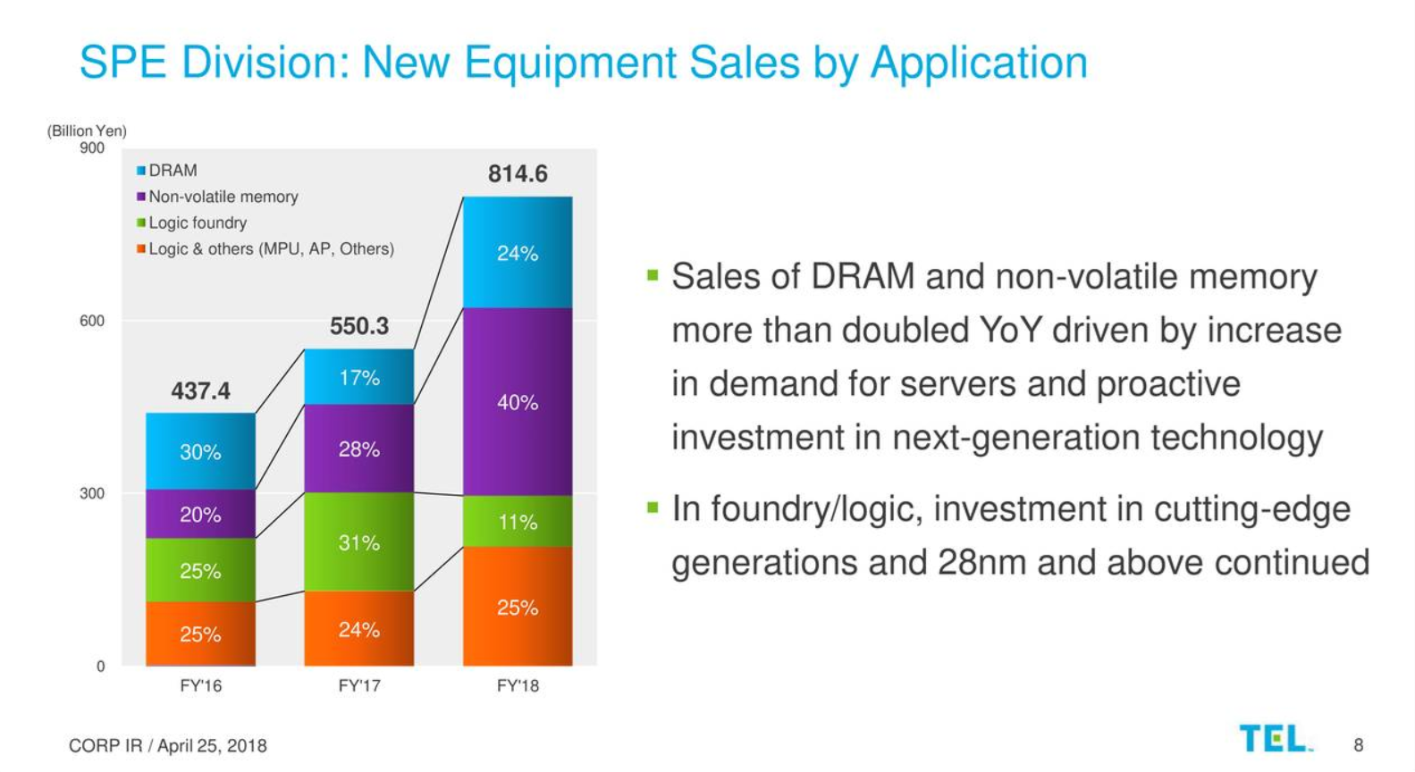
Tokyo Electron recently (APR 25, 2018) presented their Q1/2018 numbers to share holders and released a slide deck (LINK) with some interesting new numbers on market share. For the first time it seems that another OEM is up there seriously challenging ASM International on the No.1 spot in ALD Equipment market share. ASM International has dominated the ALD segment with a share of >70% in 2014, but this share has slipped down year by year and they have lost their market share to well below 50% in 2017 due to strong competition in a rapidly expanding ALD market from Tokyo Electron, Lam Research, Kokusai, The Korean OEMs (Jusung Engineering, Wonik IPS and Eugene Technology) and also to some extent by Applied Materials.
According to the latest estimate based on Gartner research (released April 18, 2018), Tokyo Electron as of 2017 holds a 31% total market share of ALD wafer based processing equipment. That should include all wafer based ALD platforms, however some companies hide their ALD revenue in the CVD segments so you can not know for sure if you don´t know the data in detail. The segments are:
ALD Tube - Large batch furnaces, typically loading 100 or more wafers
Single wafer platforms
Multi wafer platforms, spatial or multi station
TEL Market share for 2017, Based on Gartner research (TEL Q1/2018 Earnings call slide deck)
One explanation why Tokyo Electron has taken market share in ALD is because of a lot of the recent investment is coming from DRAM and 3DNAND Fabs and not Logic Fabs (see below). Traditionally Tokyo Electron has been much stronger in Memory than ASM International. Here the Japanese have very attractive tools for commodity product manufacturing (DRAM and Flash memory chips) like their ALD Large Batch Furnaces and relatively new and successful NT333 Spatial ALD platforms.
TEL sales their FY 2016 to 2018 by segment (TEL Q1/2018 Earnings call slide deck)
Also interesting is that Tokyo Electron presents a rather bright future with growth not only in DRAM and 3DNAND but also in Logic due to 10/7nm investments from the IDMs and Foundries.
ALD is a chemical deposition technique
traditionally used in the field of microelectronics and large area
displays. In recent years ALD has seen a huge evolution in terms of the
materials that can be deposited, the reactors and the applications. This
symposium aims at highlighting recent developments in the field of ALD
of functional materials and devices and to present the ALD community to
the broader materials science community.
Scope:
ALD is a Chemical Vapour Deposition technique
that is surface-limited and self-terminating. As a result, film
thickness can be controlled very precisely to the nanometer, high aspect
ratio features can be coated with a unique level of conformality, and,
film homogeneity is unrivalled. ALD, with its unique characteristics,
was developed in the 1970s to meet demands in the fields of
microelectronics and large area displays, and these have remained its
main applications, both at the lab and industrial scale, for many years.
In terms of materials, metal oxides and in particular a handful of them
(HfO2, Al2O3, TiO2, ZnO and Ta2O5)
where the sole object of ALD research. With the advent of
nanotechnology, ALD has gained momentum due to the need of controlling
and engineering surfaces and interfaces. As a result, the number of
laboratories equipped with an ALD system has increased significantly,
which has resulted in an exponential increase in the number of
publications involving ALD.
As reported by Reuters [LINK],
Intel bet the earnings expectations for the first quarter driven by the
biggest-ever quarterly jump in its data centre business and
small-but-steady growth in its personal computer business.However, Intel
also announced that they are pushing out volume production of their 10
nm Logic process to 2019, which was most recently announced for the 2nd
half of 2018. during the 1Q 2018 earnings conference calls more details
were given:
[Seeking Alpha, LINK]
"We continue to make progress on our 10-nanometer process. We are
shipping in low volume and yields are improving, but the rate of
improvement is slower than we anticipated. As a result, volume
production is moving from the second half of 2018 into 2019. We
understand the yield issues and have defined improvements for them, but
they will take time to implement and qualify. We have leadership
products on the roadmap that continue to take advantage of 14-nanometer,
with Whiskey Lake for clients and Cascade Lake for the data center
coming later this year.
Moore's Law is essential to
our strategy and our product leadership. It continues to create
significant value for Intel and our customers. While it's taking longer
and costing more to deliver and yield advanced process technologies, we
are able to optimize our process and products within the node to deliver
meaningful performance improvements.
For example,
14-nanometer process optimizations and architectural improvements have
resulted in performance gains of more than 70% since the first
14-nanometer products were launched. We combine these advances in
manufacturing technology and architecture to produce truly leadership
products. And it's that product leadership that ultimately matters most
to our customers and end users."
In
the Q&A Mr. Krzanich elaborated on the reason behind the 10 nm
push out and he explained how it is mainly due to yield issues coming
from multiple patterning (SADP and SAQP):
- Intel have 10 nm
product and process leadership and are shipping 10 nm products
today.
- Those are the densest, highest performing products out there.
- Intel is slowing the ramp down to fix yield issues related to patterning.
- In multi-multi-patterning (SAQP) there are six layers of patterning to produce a
feature.
- Intel understand the yield issues, which are tied to 10 nm being the last technology tied to not using
EUV and the amount of multi-patterning and the effects of that on
defects.
Intel’s 10 nm Platform Process was presented in detail at the IEDM 2017 (Dec 2017) “A 10nm High Performance and Low-Power CMOS Technology Featuring 3rd
Generation FinFET Transistors, Self-Aligned Quad Patterning, Contact
over Active Gate and Cobalt Local Interconnects” and you may study the details in this excellent article by Dick James [Solid State Technology, LINK]
This special topic collection is planned in collaboration with ALD 2018 and the ALE 2018 Workshop to be held in Incheon, South Korea during July 29—August 1, 2018. The Special Topic Collection will feature sections dedicated to the science and technology of atomic layer controlled deposition and to the science and technology of controlled etching of thin films. While a significant number of articles will be based on material presented at ALD 2018 and the ALE 2018 Workshop, research articles on ALD and ALE but not presented at this conference are also welcome. The special topic collection will be open to all articles on the science and technology of ALD and ALE.
Authors are encouraged to use the JVST templates. Online, you will have an opportunity to tell us that your paper is a part of the Special Topic Collection by choosing either the “ALD Special Topic Collection” or the “ALE Special Topic Collection.


%20(1).png)