Showing posts with label CMOS Scaling. Show all posts

Monday, September 23, 2019

Intel at EECS Colloquium "Moore’s Law Is Not Dead"

Intel’s Jim Keller: “We’re all building nanowires… Intel, TSMC, Samsung” Keller in his "Moore’s Law Is Not Dead" talk at UC Berkeley this week said, “We had planar transistors, we went to FinFET. We’re all building nanowires in the fab. Intel, TSMC, Samsung, everybody’s working on it. There’s a really interesting thing. While the world thinks Moore’s Law’s dead, the fabs and the technologists think it’s not and everybody’s announced now a 10-year roadmap for Moore’s Law.” 


The UC Berkeley EECS Events team has live streamed the entire talk over on YouTube and you can catch up on this fascinating, intimate little talk (below).
 
 ----------
By Abhishekkumar Thakur

Sunday, May 12, 2019

Intel 2019 Investor Meeting: 7 nm Product in 2021

Intel held its 2019 investor meeting May 8, 2019 (LINK), it's first since 2017, and CEO Bob Swan announced that Intel would launch its 7 nm process in 2021 to challenge TSMC's 5 nm products.

Intel's Xe graphics will be the leading 7 nm product, which will come on the heels of Intel's first discrete 10 nm GPU that arrives in 2020. The company also unveiled its first block diagram of the Ice Lake architecture and announced that its new 10nm Tiger Lake processors will come to market in 2020.
Source: Tom´s Hardware LINK

 (intel.com)

----------
By Abhishekkumar Thakur

Wednesday, May 8, 2019

4th CMC Conference Enabled Critical Information and Connections

Fab materials event in Albany, New York area April 25-26 featured GlobalFoundries keynote and Intel and TI presentations. Plan now for the 2020 April 23-24 event in Hillsboro, Oregon. 

(SAN DIEGO (PRWEB) May 07, 2019) Over 150 leading executives and managers within the semiconductor manufacturing ecosystem gathered on April 25th and 26th in the Albany area of New York state for an important event on fabrication (fab) materials. The fourth-annual Critical Materials Council (CMC) Conference, produced by TECHCET, included topical presentations, a fab tour, exhibits by specialty materials suppliers, and networking roundtable discussions to learn about best-practices in a pre-competitive environment. Folks who missed attending the event this year can register to access the posted presentations for a nominal fee at https://cmcfabs.org/cmc-conference-2019/.

The event opened again, as in each of the prior three years, on an extremely strong business and technology keynote address by an executive from one of the CMC Fab member companies. The 2019 CMC Conference keynote was given by Dr. John Pellerin, Deputy CTO and VP of Worldwide R&D, GlobalFoundries. Pellerin talked about how demand for new high-volume manufacturing (HVM) semiconductor devices over the next few years will drive needs for increased numbers of new specialty materials as well as volumes of existing materials in his presentation on "Materials Challenges & Opportunities in Differentiated Technologies."

In the first session of the event covering global supply-chain issues of economics and regulations, G. Dan Hutcheson, CEO of VLSI Research, presented on "Slowdown: When did it start? What drove it? And When will the recovery come?" Hutcheson showed data from leading economic indicators that the recent decline in global semiconductor fab industry revenues due to memory chip prices may have already turned around.

TECHCET Sr. Analysts Dr. Jonas Sundqvist and Terry Francis presented updated information on demand drivers and forecasts for ALD/CVD precursors and Rare Earths, respectively. Sundqvist--also leader of the Thin Film Technologies Group at Fraunhofer IKTS--focused on how new 3D memory and logic chips demand more deposition precursors such that chemical volume growth will outpace that of silicon wafers, shown in the Figure. Francis showed how "Rare Earth" elements are not so rare at the elemental level, but complex dynamics between mining and refining and capitalism have led to a situation where mainland China currently controls most of the market for elements such as lanthanum (used in advanced ICs to create CMOS logic gates). Deep dives into all such materials matters are found in the TECHCET Critical Materials Reports (CMR), and you can find all of them online at https://techcet.com/shop/

Global semiconductor silicon quarterly wafer shipments 2015-2019 in millions of square inches (MSI). (Source: TECHCET)
The 2020 spring CMC Conference is scheduled for April 24-25 in Hillsboro, Oregon. The CMC Fab members and Associate members will again gather for two days of private face-to-face meetings before attending the public CMC Conference.

In addition to the annual spring CMC Conference in the US, there is also an annual fall CMC Seminar in Asia. The 2019 CMC Seminar will be held on October 17 in Taoyuan, Taiwan. For more information on CMC events see https://techcet.com/cmc-events/.

About CMC:
The Critical Materials Council (CMC) of Semiconductor Fabricators (CMCFabs.org) is a membership-based organization that works to anticipate and solve critical materials issues in a pre-competitive environment. The CMC is a business unit of TECHCET, and includes materials supplier Associate Members.

About TECHCET:
TECHCET CA LLC is an advisory services firm focused on process materials supply-chains, electronic materials business, and materials market analysis for the semiconductor, display, solar/PV, and LED industries. Since 2000, the company has been responsible for producing the SEMATECH Critical Material Reports™, covering silicon wafers, semiconductor gases, wet chemicals, CMP consumables, Photoresists, and ALD/CVD Precursors. For additional information about reports, market briefings, CMC membership, or custom consulting please contact info(at)cmcfabs(dot)org, +1-480-332-8336, or go to http://www.techcet.com or http://www.cmcfabs.org.

Friday, March 15, 2019

Samsung’s GAA Transistor, MBCFET™ aims at Reduced Size and Increased Performance

While chipmakers are struggling with the FinFET based chip production below 5 nm process nodes, Samsung has planned to opt for GAA (gate all around) architecture. Samsung’s GAA redesigns the transistor, making it more power-efficient and better-performing than the existing Multi Bridge Channel FET (MBCFET™) that utilize stacked nanosheets. 
 
Samsung’s patented MBCFET™ is formed as a nanosheet, allowing for a larger current and simpler device integration. It allows to reduce the operating voltage below 0.75 V that had been extremely difficult with FinFET. This yields to 50% less power consumption or 30% more performance at 45% less chip area compared to 7 nm FinFET technology. Also, Samsung's GAA technology is compatible with current FinFET production line that means the today's fab running on mature process tools and methodology can be utilized for GAA transistors. Here is the infographic to learn more about how Samsung’s GAA is advancing the future of semiconductor technology.

Source: Samsung LINK

Written by : Abhishekkumar Thakur and Jonas Sundqvist
 

Wednesday, December 12, 2018

Researchers from MIT and University of Colorado produce smallest 3-D transistor yet


Using a new manufacturing technique, MIT researchers fabricated a 3-D transistor less than half the width of today’s slimmest commercial models, which could help cram far more transistors onto a single computer chip. Pictured is a cross-section of one of the researchers’ transistors that measures only 3 nanometers wide. Credits Courtesy of the researchers: Published under a Creative Commons Attribution Non-Commercial No Derivatives license


[MIT News] Researchers from MIT and the University of Colorado have fabricated a 3-D transistor that’s less than half the size of today’s smallest commercial models. To do so, they developed a novel microfabrication technique that modifies semiconductor material atom by atom.

As described in a paper presented at this week’s IEEE International Electron Devices Meeting, the researchers modified a recently invented chemical-etching technique, called thermal atomic level etching (thermal ALE), to enable precision modification of semiconductor materials at the atomic level. Using that technique, the researchers fabricated 3-D transistors that are as narrow as 2.5 nanometers and more efficient than their commercial counterparts.

Full story : MIT News LINK


Sunday, December 9, 2018

Argonne develops SIS lithography to maintain the technological progression and scaling of Moore’s Law

A manufacturing technique that could help the semiconductor industry make more powerful computer chips began in the humblest of places — at a lunch table at the U.S. Department of Energy’s (DOE) Argonne National Laboratory. 

The materials synthesis method known as sequential infiltration synthesis, or SIS, has the potential to improve not only chip manufacturing but also things like hard drive storage, solar cell efficiency, anti-reflective surfaces on optics and water-repellant car windshields. Invented in 2010 during a lunchtime conversation between Argonne scientists Seth Darling and Jeffrey Elam and two of their postdoctoral researchers, use of the method has grown in recent years.


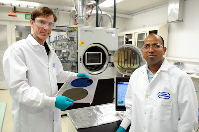
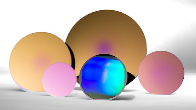
Top: Jeff Elam and Anil Mane, co-inventor on the SIS for lithography method and Principal Materials Science Engineer in Argonne’s Applied Materials Division. Bottom: Silicon wafers, ranging in size from 4” to 12” diameter, that have been treated using Argonne’s sequential infiltration synthesis method (Credit : Argonne National Laboratory).

The method was based on the group’s discussion of atomic layer deposition, or ALD, a thin film deposition technique that uses alternating chemical vapors to grow materials one atomic layer at a time. Darling, director of the Institute for Molecular Engineering at Argonne and the Advanced Materials for Energy-Water Systems Energy Frontier Research Center, recently used that technique to add a water-loving metal oxide coating to filters used in the oil and gas industry which prevents the filters from clogging.

“It worked beautifully on the first try.” — Seth Darling, director of Argonne’s Institute for Molecular Engineering and the Advanced Materials for Energy-Water Systems Energy Frontier Research Center

But as the group talked, they started speculating about taking ALD to a new level, said Darling.

“We said ​‘Wouldn’t it be neat if we could grow one material inside another material like a polymer (a string of many combined molecules) instead of on top of it?’” Darling said. ​“We first thought ​‘This isn’t going to work,’ but, surprisingly, it worked beautifully on the first try. Then we began imagining all of the different applications it could be used for.”

The research was funded by the DOE Office of Science, Basic Energy Sciences Program as well as the Argonne-Northwestern Solar Energy Research Center, a DOE Office of Science-funded Energy Frontier Research Center.


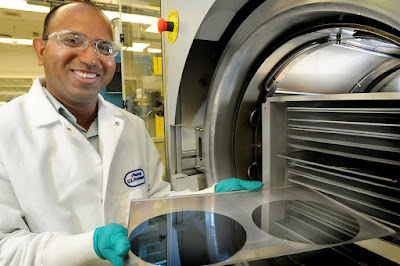
Anil Mane unloding wafers processed in a BENEQ TFS 500 ALD reactor at Argonne’s Applied Materials Division. (Credit : Argonne National Laboratory).

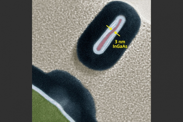
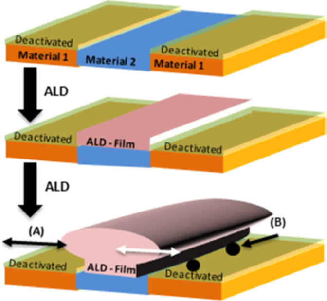
SIS is similar to ALD on a polymer surface, but in SIS the vapor is diffused into the polymer rather than on top of it, where it chemically binds with the polymer and eventually grows to create inorganic structures throughout the entire polymer bulk.

Using this technique, scientists can create robust coatings that can help the semiconductor manufacturing industry etch more intricate features on computer chips, allowing them to become even smaller or to add extra storage and other capabilities. They can also tailor the shape of various metals, oxides and other inorganic materials by applying them to a polymer with SIS and then removing the remains of the polymer.

“You can take a pattern in a polymer, expose it to vapors and transform it from an organic material to an inorganic material,” said Elam, director of Argonne’s ALD research program, referring to the way the method can use polymers and a vapor to basically mold a new material with specific properties. ​“It’s a way to use a polymer pattern, and convert that pattern into virtually any inorganic material.”

The technology’s potential spans beyond semiconductors. It could be used to advance products in different industries, and Argonne would be delighted to work with commercialization partners who can take the invention and incorporate it in existing products - or invent new applications to benefit U.S. economy, said Hemant Bhimnathwala, a business development executive at Argonne.

“You can use SIS to create a film, you can put it on a metal, you can create this on glass or put it on a glass windshield to make it water repelling to the point where you don’t need wipers,” Bhimnathwala said.

The way the scientists invented the technique — through that lunch meeting — was also a bit unusual. New discoveries often come about by accident, but not usually by spitballing ideas over lunch, Elam said.

“Occasionally, if you’re watching intently, you can see something else there and discover something new and unexpected,” Elam said. ​“That doesn’t happen very often, but when it does, it’s great.”

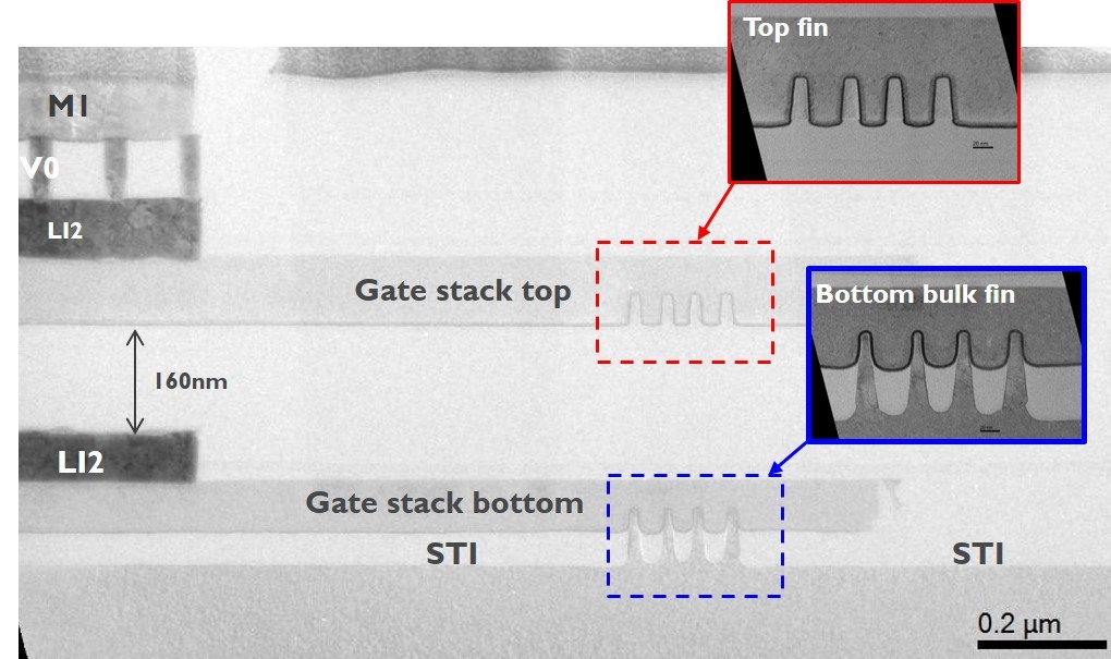
The technique also addresses a specific concern in the semiconductor manufacturing industry, pattern collapse, which means the collapse of tiny features used to create electrical components on a computer chip, rendering it useless.

When a pattern is etched on a silicon chip in the chip-making process, an etch-resistant surface is used as a protective coating to mask those regions you do not want to remove. But the etch-resistant coatings commonly used today wear away very quickly, which has prevented chip manufacturers from making components with deeply etched features, Darling said.

With SIS, inorganic vapor coatings can be engineered to provide greater protection of vertical features, allowing deeper etches and the integration of more components on each chip.

“Features on chips have gotten extremely small laterally, but sometimes you also want to make them tall,” Darling said. ​“You can’t make a tall feature if your resist etches away quickly, but with SIS it’s easy.”

Similarly, the technique can be used to manipulate magnetic recording on hard drives or other storage devices, allowing them to increase storage while also getting smaller, Darling said.

Another possibility for the technology is to control how much light bounces off a glass or plastic surface. Using SIS, scientists can engineer surfaces to be almost entirely non-reflective. Using this strategy, scientists can improve performance of solar cells, LEDs and even eyeglasses.

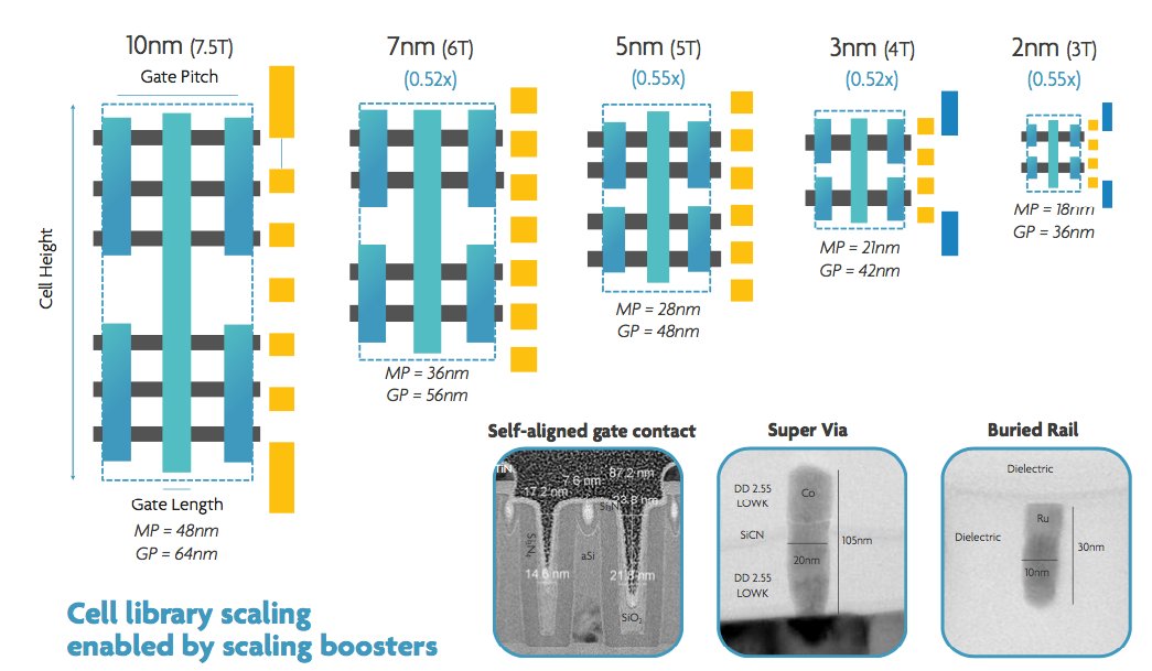
“There are also a lot of applications in electronics,” Elam said. ​“You can use it to squeeze more memory in a smaller space, or to build faster microprocessors. SIS lithography is a promising strategy to maintain the technological progression and scaling of Moore’s Law.”

The team’s research on the technology has been published in The Journal of Materials Chemistry, The Journal of Physical Chemistry, Advanced Materials and The Journal of Vacuum Science & Technology B.

Argonne is looking for commercial partners interested in licensing and developing the technology for more specific uses. Companies interested in leveraging Argonne’s expertise in SIS should contact partners@​anl.​gov to learn more and discuss possible collaborations.


Top: Seth Darling, Scientist and Director of the Institute for Molecular Engineering at Argonne National Laboratory. Bottom: Jeff Elam, Senior Chemist in Argonne’ Applied Materials Division (bottom). Picture Credit : Argonne National Laboratory.

Friday, November 23, 2018

CMC Conference Call for Papers, April 25-26, 2019 in Saratoga Springs, NY, USA

The Critical Materials Council (CMC) Conference Committee has issued a call for presentations for the 4th annual public CMC Conference to be held April 25-26, 2019 in Saratoga Springs, NY, USA, following the private CMC face-to-face meetings (April 23-24). The theme of this year’s conference is:

“Materials for Advancing Processes & Technologies”
Keynote: DR. JOHN PELLERIN, Deputy CTO & VP of Worldwide R&D, GlobalFoundries

Three sessions will cover:

I. Global supply-chain issues of economics and regulations,
II. Immediate challenges of materials & manufacturing, and
III. Emerging materials in R&D and pilot fabrication.

 
To encourage the free exchange of the most current pre-competitive information the CMC Conference only requires that speakers submit an abstract for review, and if accepted, presentation slides. No formal paper is required. To submit a 25 min. presentation for consideration, please send a 1-page abstract by January 15, 2019 to cmcinfo@techcet.com.

Attendees will include industry experts handling supply-chains, business-development, R&D, and product management, as well as academics and analysts. CMC member companies will be attending this meeting, as it is an important part of their membership.

On behalf of the CMC Conference Committee,
Jonas Sundqvist, Ph.D., Karey Holland, Ph.D. and Ed Korczynski

Monday, November 19, 2018

15 nm resolved patterns in Selective Area Atomic Layer Deposition

Here is an impressive and fundamental paper on selective area atomic layer deposition (SA-ALD)or just area selective deposition (ASD) that some prefer to call it.

The researchers at IBM has devleoped a bottom up approach on 300 mm pattern wafers that had been fabricated using standard trench first metal hardmask damascene scheme to create a line pattern of 36 nm pitch with single EUV exposures using low-k OMCTS 2.7 as the dielectric.
 
By deactivating ond surface with self-assembled monolayers (SAMs, Octadecylphosphonic acid) leaving another surface active for ALD processing (ZnO) they were able to produce 15 nm resolved patterns. One of the biggest challenges in the implementation of SA-ALD is the ability to maintain pattern fidelity and reduce defects during the ALD process (ZnO). 
 
Thank you Henrik Pedersen for sharing this paper!


Deactivating material is used to block one surface from ALD film growth. (A) ALD eventually leads to overgrowth of the film onto deactivated areas. (B) Defects in the deactivation layer can lead to the formation of locally deposited material. Published with permission from ACS Appl. Mater. Interfaces, 2018, 10 (44), pp 38630–38637 Copyright 2018 American Chemical Society.

Fifteen Nanometer Resolved Patterns in Selective Area Atomic Layer Deposition—Defectivity Reduction by Monolayer Design

Rudy Wojtecki, Magi Mettry, Noah F. Fine Nathel, Alexander Friz, Anuja De Silva, Noel Arellano, and Hosadurga Shobha
ACS Appl. Mater. Interfaces, 2018, 10 (44), pp 38630–38637
DOI: 10.1021/acsami.8b13896

Saturday, November 10, 2018

Directed self-assembly of block copolymers for 7 nanometre FinFET technology and beyond

Globalfoundries recently announced that they have dropped all plans on putting 7 nm FinFET technology in production (LINK). Presumably this means that any advanced development for 7nm and beyond patterning has been stopped as well. In any case here is an excellent publication submitted before that announcment coming from the collaborative development from some of the most advanced semiconductor development centers in the USA - IBM Research at Albany NanoTech, TEL Technology Center, America in Albany, GlobalFoundries, and IBM Research TJ Watson in Yorktown Heights and IBM Research Almaden, San Jose.


They use different versions of directed self assembly (DSA) of block co-polymers (BCP) and spacer defined double patterning. ALD is used for spacers as well as very thin ALD SiN hardmasks. All this is all done without EUV like in the Samsung 2nd Generation 7nm FinFET or self aligned quadruple patterning (SAQP) like in the Intel 10 nm FinFET) - Impressive!

Some details are given in the Supplementary info (below).

Directed self-assembly of block copolymers for 7 nanometre FinFET technology and beyond


Nature Electronics volume 1, pages562–569 (2018)

Supplementary information : LINK (OPEN)


Friday, November 9, 2018

Samsung will give insights to their 3nm CMOS technology at IEDM2018

The 64th IEDM conference will be held December 1-5, 2018 in San Francisco (LINK). This year Samsung will give insights to their 3nm CMOS technology that will feature the so calle gate-all-around (GAA) transistors. The GAA is trasistors ar realized by having channels made from horizontal layers of nanosheets that are completely surrounded by gate structures. 

Samsung has recently stated (LINK) that they have started wafer production on its new 7LPP node (FinFET). According to the press release the process uses EUV lithography technology and demonstrates that Samsung's Foundry can follow its roadmap reaching down to 3 nm.


Samsung Foundry Roadmap as shown at SFF Japan 2018.
 
Samsung refers to this architecture as a Multi-Bridge-Channel architecture, and claims "that it is highly manufacturable as it makes use of ~90% of the company’s existing FinFET fabrication technology, requiring only a few revised photomasks" (LINK). 
 
Paper #28.7, "3nm GAA Technology Featuring Multi-Bridge-Channel FET for Low-Power and High-Performance Applications," G. Bae et al, Samsung


Imec to present Highest-Density 3DS Stacked FinFETs at IEDM 2018

Here is an interesting paper to be presented by Imec at the upcoming IEDM 2018 in San Fransisco. Imec has managed to stack the complete FinFET front end module on top of a "standard" bulk silicon FinFET Module demonstrating also good threshold voltage tuning, reliability and low-temperature performance. 

So just imagine if this would be used in high volume manufacturing - it would mean that all those ALD processes used in patterning and for the high-k metal gate module, spacers, local interconnect etc. etc. would come twice meaning a 2X need for ALD process chambers. And lets say you can run this twice - is there any reasons why you can´t run it yet another time? Woah!

Also as a note, Imec is here using a LaSiOx layer an a dipole inserted in the HKMG stack - presumably it is an ALD process since it will have to conformally coat this fins and ensure precise thickness control and uniformity.

So just enjoy seeing double - it is Friday!

Paper #7.1, “First Demonstration of 3D Stacked FinFETs at a 45nm Fin Pitch and 110nm Gate Pitch Technology on 300mm Wafers,” A. Vandooren et al, Imec

Highest-Density 3DS Stacked FinFETs: Imec researchers will report on 3D stacked FinFETs that have the tightest pitches ever reported in such a stacked architecture – 45nm fin pitch and 110nm gate pitch. The 3D architecture makes use of a sequential integration process yielding tight alignment between very thin top and bottom Si layers. The junction-less devices in the top layer were fabricated and transferred using low-temperature (≤525ºC) processes to avoid performance degradation, and a 170nm dielectric was used to bond the two wafers. The top layer is so thin that the bottom layer could be patterned right through it by means of 193nm immersion lithography, which connects the two via local interconnect. The researchers evaluated various gate stacks, ultimately choosing TiN/TiAl/TiN/HfO2 with a LaSiOx dipole inserted into the stack. The combination demonstrated good threshold voltage tuning, reliability and low-temperature performance.

At left above is a cross-sectional electron microscope image of the fabricated 3D stacked FinFETs along fins and across gates, showing the tight alignment achieved by the top processed layers (Gate Li1, Li2) toward the bottom layers. At right is a cross-sectional image of the final devices across fins with the gates covering the fins.


“First Demonstration of 3D Stacked FinFETs at a 45nm Fin Pitch and 110nm Gate Pitch Technology on 300mm Wafers,” A. Vandooren et al, Imec (IEDM 2018 Press kit)

Source: IEDM Press kit (LINK)

Friday, April 27, 2018

Intel shifts high volume 10 nm shipments to 2019 due to yield issues from multi-patterning

As reported by Reuters [LINK], Intel bet the earnings expectations for the first quarter driven by the biggest-ever quarterly jump in its data centre business and small-but-steady growth in its personal computer business.However, Intel also announced that they are pushing out volume production of their 10 nm Logic process to 2019, which was most recently announced for the 2nd half of 2018. during the 1Q 2018 earnings conference calls more details were given:

[Seeking Alpha, LINK] "We continue to make progress on our 10-nanometer process. We are shipping in low volume and yields are improving, but the rate of improvement is slower than we anticipated. As a result, volume production is moving from the second half of 2018 into 2019. We understand the yield issues and have defined improvements for them, but they will take time to implement and qualify. We have leadership products on the roadmap that continue to take advantage of 14-nanometer, with Whiskey Lake for clients and Cascade Lake for the data center coming later this year.

Moore's Law is essential to our strategy and our product leadership. It continues to create significant value for Intel and our customers. While it's taking longer and costing more to deliver and yield advanced process technologies, we are able to optimize our process and products within the node to deliver meaningful performance improvements.

For example, 14-nanometer process optimizations and architectural improvements have resulted in performance gains of more than 70% since the first 14-nanometer products were launched. We combine these advances in manufacturing technology and architecture to produce truly leadership products. And it's that product leadership that ultimately matters most to our customers and end users."

Brian M. Krzanich - Intel Corp.

Earnings call slides [Seeking Alpha, LINK]

In the Q&A Mr. Krzanich elaborated on the reason behind the 10 nm push out and he explained how it is mainly due to yield issues coming from multiple patterning (SADP and SAQP):

- Intel have 10 nm product and process leadership and are shipping 10 nm products today. 
- Those are the densest, highest performing products out there.
- Intel is slowing the ramp down to fix yield issues related to patterning.
- In multi-multi-patterning (SAQP) there are six layers of patterning to produce a feature. 
- Intel understand the yield issues, which are tied to 10 nm being the last technology tied to not using EUV and the amount of multi-patterning and the effects of that on defects.


Intel’s 10 nm Platform Process was presented in detail at the IEDM 2017 (Dec 2017) “A 10nm High Performance and Low-Power CMOS Technology Featuring 3rd Generation FinFET Transistors, Self-Aligned Quad Patterning, Contact over Active Gate and Cobalt Local Interconnects” and you may study the details in this excellent article by Dick James [Solid State Technology, LINK]

Media coverage:
 
The Register
 

Thursday, January 25, 2018

High Dielectric Constant Materials for Nanoscale Devices and Beyond

Here is a nice review on the introduction of high-k materials in the semiconductor industry and a future outlook by Prof. Hiroshi Iwai at Tokyo and Prof. Akira Toriumi Institute of Technology and their partner Prof. Durga Misra at New Jersey Institute of Technology. Thank you for sharing this one Rob Clark! The paper is part of a winter special issue in Interface (by ECS) with focus on "Importance of dielectric science"  and is free for download.


The authors conclude that:
  • The step coverage advantage of atomic layer deposition (ALD and is possible for, high‑k migration to FinFET CMOS technology.
  • The use of high‑k on new semiconductor substrates such as III-V, Ge and 2D materials is currently being investigated and faces many challenges. 
  • The discovery of ferroelectric properties of HfO2 makes it viable for more potential applications.


High Dielectric Constant Materials for Nanoscale Devices and Beyond
Hiroshi Iwai, Akira Toriumi and Durga Misra

Electrochem. Soc. Interface Winter 2017 volume 26, issue 4, 77-81

Abstract: Tremendous progress of CMOS integrated circuits have been conducted by the down-scaling or the miniaturization of MOSFETs (Metal Oxide Semiconductor Field Effect Transistors). Ten years, ago, the huge direct-tunneling gate leakage current through the thin gate SiO2 film of 1 nm thickness made it impossible to further scale-down the MOSFETs, and replacing the SiO2 by HfO2-based higher-dielectric constant (high-k) material was the solution. In this paper, the history of high-k gate insulator film development and two topics from recent research results regarding ferroelectricity and reliability are described.

Tuesday, January 23, 2018

CMC Conference 2018 Keynote by Intel Litho VP

Register now for early-bird rate to April 24-25 event in Phoenix area
SAN DIEGO, Jan. 23, 2018 /PRNewswire-iReach/ -- TECHCET CA—the advisory service firm providing electronic materials information—and the Critical Materials Council (CMC) of semiconductor fabricators announce that David Bloss, Vice President of Technology and Manufacturing Group, and Director of Lithography Technology Sourcing in Global Supply Management, Intel Corporation, will provide the keynote address at the next CMC Conference to be held April 24-25, 2018 in Chandler, Arizona (http://cmcfabs.org/cmc-events/). Building on the success of the prior CMC Conferences, the 2018 event will feature presentations by technologists from leading fabs, OEMs, materials suppliers, and analysts.


Following the annual members-only CMC meeting held earlier in the week, the 2017 CMC Conference is open to the public. Business drives our world, but technology enables the profitable business of manufacturing new semiconductor devices, and new devices need new materials. Presentation sessions will focus on the following topics:
  • Global Issues & the Supply Chain,
  • Immediate Challenges of Materials & Manufacturing, and
  • Emerging Materials Challenges.
To register for the conference at the early-bird rate of $375 by March 15, 2018—after which the price increases to $450—please got to the website http://cmcfabs.org/registration/.

ABOUT CMC:  The Critical Materials Council (CMC) of Semiconductor Fabricators (CMCFabs.org) is a membership-based organization that works to anticipate and solve critical materials issues in a pre-competitive environment. The CMC is a unit of TECHCET.

ABOUT TECHCET:  TECHCET CA LLC is an advisory service firm focused on process materials supply chains, electronic materials technology, and materials market analysis for the semiconductor, display, solar/PV, and LED industries. Since 2000, the company has been responsible for producing the SEMATECH Critical Material Reports, covering silicon wafers, semiconductor gases, wet chemicals, CMP consumables, Photoresists, and ALD/CVD Precursors. For additional information about these reports or CMC Fabs membership please contact Diane Scott at info@cmcfabs.org +1-480-332-8336, or go to www.techcet.com or www.cmcfabs.org.

Media Contact: Lita Shon-Roy, TECHCET CA LLC, 1-480-382-8336, info@techcet.com

Monday, January 22, 2018

Imec present roadmap down to 20 Ångström logic devices

From now on I think that it is time to start using Ångström instead of Nanometer (nm) when talking about leading edge CMOS and Memory.  At SEMI:s ISS 2018 (Industry Strategy Symposium) last week Luc van den Hove, Chief Executive Officer and President of Interuniversity MicroElectronics Center (IMEC) presented their roadmap for what future Logic nodes might look like going down to 2 nm that is 20 Ångström.

Key interconnect technologies named "scaling boosters" to reach down to 2 nm may be :
  • Continued scaling of self-aligned contacts
  • Cobalt "Super Via" 20 nm wide
  • Burried Ruthenium Rails only 10 nm wide, which seems to be a evolution of the tungsten burried Word Lines and Bitlines introduced by Qimonda for DRAM (65nm in 2009) except offcourse these rails are burried in a dielectric which will  make it stackable. 


Imec Logic roadmap and technologies, Picture from Twitter (LINK)


Besides the interconnect technologies the presentation showed evolution from FinFETs to nanowire FETs and Imecs latest technology development in 300 mm wafer processing technology:
  • Introduction of triple pattering (Much More ALD!)
  • EUV Litography and the introduction Carbon Nano Tube CNT Pellicle for EUV mask protection
  • Smoothening technology in patterning like Atomic Layer Etching for improving the local critical dimension uniformity (LCDU) down from 2.7 to 1.4 nm
In the case of memory technology Imec now focuses on 4 non-volatile types of memory cells besides DRAM and 3DNAND Flash:
  • STTRAM - spin transfer torque magnetoresistive random-access memory
  • RRAM - resistive random-access memory
  • FeRAM - ferroelectric random-access memory (should be renamed DD-RAM for Dresden)
  • SOTRAM - Spin Orbit Torque random-access memory


Sunday, January 21, 2018

The use of ALD in Intel & Globalfoundires leading edge technology

At IEDM 2017 in San Fransisco in December in the Advanced Platform Technologies session Intel and Globalfoundries presented their 10 nm and 7 nm technology, respectively. Intel and Globalfoundries (as well as TSMC) are using different node names, however these two nodes have similar density and can be compared side by side. In a recent article by Scotten Jones in SemiWiki the Intel 10 nm vs. Globalfoundries 7 nm are compared based on previous disclosures, interviews and the IEDM 2017 papers.

This is a very interesting article for those of you who like to dig in deeper into the most leading edge technologies in production 2018 and you can imagine that none of this would have been possible without ALD:
  • Both Intel and Globalfoundries are using SAQP for the fins patterning, presumably using PEALD liners that are on offer from ASM International, Applied Materials and others.
  • Intel is using its fifth generation of high-k metal gates (HKMG). As you know, Intel introduced HKMG in 2007 at 45 nm ahead of the rest of the industry. Whereas Globalfoundries is at its 4th generation, depending on how you count. The IBM Alliance started of with MOCVD High-k (Tokyo Electron at AMD/Globalfoundries and Applied Materials at STMicro) for 32 nm and then moved to ALD high-k (ASM Pulsar 3000) and I am assuming still uses that ALD work horse.
  • In the case of Intel, the contact metal stack also includes a conformal titanium layer and it remains to be seen if this is possibly an ALD process - we know that Prof. Winter has showed amazing progress in thermal ALD of Ti-rich layers, but this could as well be PECVD if the thermal budget allows or some sneaky trics from the Applied Materials PVD magicians in Santa Clara.
  • In the case of Cobalt, we have to assume that the Intel Cobalt vias and lines are not realized by CVD. They are most probably deposited by a Electroless Deposition (ELD) process. ELD Cobalt is claimed to provide void-free bottoms-up pre-filling of vias and contacts as presented by Imec and Lam Research (Solid State Technology LINK) some time ago. In case of the Cobalt liners and Caps used to encapsulate the copper vias and lines by both Intel and Globalfoundries it is safe to assume that these are CVD processes using Applied Materials Cobalt CVD chambers (Endura Volta LINK). Here we know about published work from ALD Cobalt and selective ALD Cobalt that may or may not have come into play (Marissa Kerrigan et al Chem. Mater., 2017, 29 (17), pp 7458–7466)
  • Further up in the Copper layers, the Globalfoundries technology also offer MIM Capacitors that can be either for decoupling or potentially also include embedded DRAM memory cells in a via integration. These have in many cases in older nodes been realized by using low thermal budget ALD or PEALD ZrO2 node dielectric (e.g. from STMicro, Renesas).
  • Adding to all this, there are a multitude of liners, diffusion barriers as well as multiple patterning in BEOL where ALD may have come into play. It is safe to assume that for each node there is more ALD in play.
These speculations are open for debate! :-)

IEDM 2017 - Intel Versus GLOBALFOUNDRIES at the Leading Edge 

by Scotten Jones Published on 12-22-2017 08:00 AM

Article: LINK

Intel 10 nm vs. Globalfoundries 7 nm Fins beautifully conformally coverd by ALD High-k/Metal Gate stacks (SemiWiki).
 

Tuesday, January 2, 2018

Single Atomic Layer Ferroelectric on Silicon by PVD ZrO2


A team of mainly US based researchers from (Yale, MIT, Université de Genève and Globalfoundries) have been able to scale down ferroelectric ZrO2 to only one atomic layer on silicon using PVD. This record breaking thin monolayer ferroelectric allows for more aggressively scaled devices than bulk ferroelectrics as compared to the most current 5–10 nm thick layers based on e.g. Si:HfO2 and HfZrOx. 

They found that:
  • single atomic layer ZrO2 exhibits ferroelectric switching behavior when grown with an atomically abrupt interface on silicon
  • ZrO2 gate stack demonstrate that a reversible polarization of the ZrO2 interface structure couples to the carriers in the silicon.
Single Atomic Layer Ferroelectric on Silicon
Mehmet Dogan, Stéphanie Fernandez-Peña, Lior Kornblum, Yichen Jia, Divine P. Kumah, James W. Reiner, Zoran Krivokapic, Alexie M. Kolpak, Sohrab Ismail-Beigi, Charles H. Ahn, and Frederick J. Walker

Nano Lett., Article ASAP, DOI:10.1021/acs.nanolett.7b03988

Abstract: A single atomic layer of ZrO2 exhibits ferroelectric switching behavior when grown with an atomically abrupt interface on silicon. Hysteresis in capacitance–voltage measurements of a ZrO2 gate stack demonstrate that a reversible polarization of the ZrO2 interface structure couples to the carriers in the silicon. First-principles computations confirm the existence of multiple stable polarization states and the energy shift in the semiconductor electron states that result from switching between these states. This monolayer ferroelectric represents a new class of materials for achieving devices that transcend conventional complementary metal oxide semiconductor (CMOS) technology. Significantly, a single atomic layer ferroelectric allows for more aggressively scaled devices than bulk ferroelectrics, which currently need to be thicker than 5–10 nm to exhibit significant hysteretic behavior (Park, et al. Adv. Mater. 2015, 27, 1811).

Reprinted with permission from (Single Atomic Layer Ferroelectric on Silicon, M. Dogan et al, Nano Letters, Dec 2017). Copyright (2018) American Chemical Society.

High‐resolution STEM image and EDX intensity profiles of Si, Al and Zr. The Supporting Information is available free of charge on the ACS Publications website at "Single Atomic Layer Ferroelectric on Silicon" https://figshare.com/collections/Single_Atomic_Layer_Ferroelectric_on_Silicon/3961401