Showing posts with label CMOS Scaling. Show all posts

Monday, January 1, 2018

Purdue University demonstrate negative capacitance MoS2 transistors using ferroelectric HfZrOx

WEST LAFAYETTE, Ind. –  Researchers have experimentally demonstrated how to harness a property called negative capacitance for a new type of transistor that could reduce power consumption, validating a theory proposed in 2008 by a team at Purdue University.

The researchers used an extremely thin, or 2-D, layer of the semiconductor molybdenum disulfide to make a channel adjacent to a critical part of transistors called the gate. Then they used a “ferroelectric material” called hafnium zirconium oxide to create a key component in the newly designed gate called a negative capacitor.

A new type of transistor (a) harnesses a property called negative capacitance. The device structure is shown with a transmission electron microscopy image (b) and in a detailed “energy dispersive X-ray spectrometry” mapping (c). (Purdue University photo/Mengwei Si)

Capacitance, or the storage of electrical charge, normally has a positive value. However, using the ferroelectric material in a transistor’s gate allows for negative capacitance, which could result in far lower power consumption to operate a transistor. Such an innovation could bring more efficient devices that run longer on a battery charge.

Thursday, December 14, 2017

Globalfoundrfies to use quad patterning and Cobalt contacts for 7nm

ZDNet reports: At IEDM Globalfoundries presented details of its 7nm process which promises a significant increase in density, performance and efficiency in comparison to the 14nm technology used to manufacture AMD processors, IBM Power server chips and other products. GlobalFoundries will start 7nm production using current lithography tools, though it plans to quickly move to next-generation EUV lithography to cut costs

Based on GlobalFoundries latest generation of 3D or FinFET transistors, the 7LP process has a fin pitch (the distance between the conducting channels) of 30nm, gate pitch of 56nm and a minimum metal pitch of 40nm--all of which are "significantly scaled from 14nm." GlobalFoundries said it tuned the fin shape and profile for best performance, but did not provide measurements for the width or height of the fins. The smallest high-density SRAM cell measures 0.0269 square microns.
 
Like Intel, GlobalFoundries will use self-aligned quad patterning (SAQP) to fabricate the fins, as well as double-patterning for metal layers, and has introduced cobalt metal contacts to reduce resistance.


Saturday, November 25, 2017

The 7nm race by TSMC and Samsung - EUV or not EUV

According to industry sources on October 19, Samsung Electronics is considering a plan to purchase 10 extreme ultraviolet (EUV) lithography tools from the Netherlands-based ASML, the biggest semiconductor equipment maker in the world. To put tha in perspective - ASML believes that it can produce about 12 EUV lithography tools this year. It is the only company that manufactures EUV lithography tools in the world.

Sales in ALD and Etch equipment have been boosted by multiple patterning technologies based on Immersion lithography, both for Logic/Foundry and Memory. Maybe as much as 1/3 of the single/multi wafer ALD equipment market is patterning related. The last two years or so analyst have been busy trying to figure out the impact on deposition and etch equipment sales if/when EUV is introduced. Here is a recent take down by Seeking Alpha (LINK). My view is that scaling is based on symbiotic use of the latest technologies and multiple patterning and EUV will co-exist and keeping the scaling path alive. In addition, scaling opens new opportunities for ALD, ALEtch and future use of selective growth technologies with atomic scale precision. According to recent reports the ALEtch market segment is now considerd an actual segment by itself and has entered HVM (LINK).
Fudzilla reports: Korean based ETNews has mentioned that Qualcomm 7nm manufacturing has been a big win for TSMC while two other US and China customers chose Samsung’s 7nm. TSMC traditionially have dibs on Nvidia and MediaTek according to the report.

Qualcomm and Broadcom, according to the report are designing their next generation chips with TSMC’s7-nano PDK. The reason why Qualcomm went with 7nm with TSMC is the fact that the fab uses normal steppers while Samsung wants to make its 7nm with more bold and riskier EUV (Extreme Ultraviolet) photolithography technology.

View of Samsung Electronics’ Hwasung 17 line. It is expected that Samsung Electronics will build a new 7-nano plant on a nearby site according to ETNews.

Samsung is expected to be later to the 7nm game and early adopters had to go with TSMC. EUV is still technology that is not entirely ready for the mass market and there is a disagreement weather you should need to use Extreme Ultraviolet light manufacturing with 7nm or first with 5nm. Obviously the two main fabs disagree while GlobalFoundries cooperates and shares technology with Samsung, and will have Samsung to rely upon for 7nm.

Full article: Qualcomm 7nm made by TSMC [LINK]
ETNews original source: Samsung Electronics Close to Securing Two New Customers for Its 7-Nano Foundry[LINK]
Business Korea: Keeping Leadership in 7-nano Era Samsung Electronics Seeks to Buy Up Next-gen Semiconductor Mfg Equipment

Sunday, October 22, 2017

Intel to present 10 nm Logic with 3rd gen FinFET and 2 level Cobalt interconnect

IEDM 2017 Announcement (LINK, Press kit): Intel researchers will present a 10nm logic technology platform with excellent transistor and interconnect performance and aggressive design-rule scaling. They demonstrated its versatility by building a 204Mb SRAM having three different types of memory cells: a high-density 0.0312µm2 cell, a low voltage 0.0367µm2 cell, and a high-performance 0.0441µm2 cell. The platform features 3rd-generation FinFETs fabricated with self-aligned quadruple patterning (SAQP) for critical layers, leading to a 7nm fin width at a 34nm pitch, and a 46nm fin height; a 5th-generation high-k metal gate; and 7th-generation strained silicon. There are 12 metal layers of interconnect, with cobalt wires in the lowest two layers that yield a 5-10x improvement in electromigration and a 2x reduction in via resistance. NMOS and PMOS current is 71% and 35% greater, respectively, compared to 14nm FinFET transistors. Metal stacks with four or six workfunctions enable operation at different threshold voltages, and novel self-aligned gate contacts over active gates are employed.

The graph on the left shows that the new platform maintains traditional scaling trends, while the photomicrograph on the right shows the platform’s 12-layer interconnect stack.


Reference: Paper 29.1, “A 10nm High Performance and Low-Power CMOS Technology Featuring 3rd-Generation FinFET Transistors, Self-Aligned Quad Patterning, Contact Over Active Gate and Cobalt Local Interconnects,” C. Auth et al, Intel

2017 IEEE International Electron Devices Meeting
December 2-6, 2017
Hilton San Francisco Union Square
333 O’Farrell Street
San Francisco, CA 94102

Tuesday, August 22, 2017

Woah - Hafnium oxide as gate dielectric scales also in the 2D world

Hafnium oxide high-k dielectrics deposited by atomic layer deposition have been used in DRAM since 2004 (Samsung 90 nm) and 2007 in high performance CMOS logic (Intel 45 nm). Later the DRAM high-k dielectric was replaced by a zirconium oxide based material but for logic hafnium oxide has remained the material of choice for the high-k metal gate stack by toping off the native oxide of silicon with its higher k-value. Hafnium oxide even survived the transition to narrow 3D FinFET devices and is also the main contender for silicon based Nano Wire FETs. However, recent research in alternative 2D channel materials such as graphene, molybdenum disulfide and others has created a totally new situation where hafnium oxide finds it difficult to compete as the material of choice for the gate stack dielectric. 

Until now that is, because just recently some clever researchers at Stanford has presented an new all hafnium channel and dielectric combo using hafnium diselenide and the natural native oxide of that - ta da - hafnium oxide. Apparently the zirconium version is also brought into play but let us see about that...

You can read all about it in this online article published by Stanford, which also leads you to the original scientific references and journal publications.

New ultrathin semiconductor materials exceed some of silicon’s ‘secret’ powers, Stanford engineers find

The next generation of feature-filled and energy-efficient electronics will require computer chips just a few atoms thick. For all its positive attributes, trusty silicon can’t take us to these ultrathin extremes.

Now, electrical engineers at Stanford have identified two semiconductors – hafnium diselenide and zirconium diselenide – that share or even exceed some of silicon’s desirable traits, starting with the fact that all three materials can “rust.”


TEM cross-section of an experimental chip, the bands of black and white reveal alternating layers of hafnium diselenide – an ultrathin semiconductor material – and the hafnium dioxide insulator. (Image credit: Michal Mleczko)

Thursday, August 3, 2017

Coventor solutions to atomic level challenges in semiconductor technology

Atomic Level Processing technology like ALD and ALE are crucial for current and coming nodes in both logic and memory. So for you atomic level people it may be interesting to keep a close track of the current challenges and solutions  in scaling and patterning. Here are three interesting articles by Coventor covering this topics (from the Coventor August 2017 news letter).

What drives SADP BEOL variability (LINK)?


Figure from Coventor August 2017 newsletter


Until EUV lithography becomes a reality, multiple patterning technologies such as triple litho-etch (LELELE), self-aligned double patterning (SADP), and self-aligned quadruple patterning (SAQP) are being used to meet the stringent patterning demands of advanced back-end-of-line (BEOL) technologies. In this blog, we modeled SADP process variability to try to understand the effect of this variability on BEOL and RC performance.

How small variations in photoresist shape significantly impact multi-patterning yield (LINK)

 Figure from Coventor August 2017 newsletter
Things were easy for integrators when the pattern they had on the mask ended up being the pattern they wanted on the chip. Multi-patterning schemes such as Self-Aligned Double Patterning (SADP) and Self-Aligned Quadruple Patterning (SAQP) have changed that dramatically. In this blog, we look at how small variations in photoresist shape can significantly impact multi-patterning yield.

Problems and Solutions at 7nm (LINK)

As we approach 7nm and lower technology nodes, lithography, patterning, material and interconnect challenges abound. David Fried, Chief Technology Officer of Coventor, addresses these challenges in a video interview with Ed Sperling of Semiconductor Engineering. David also reviews the problems that we are facing at both 7nm and 5nm and proposes some potential solutions. 


Movie from Coventor August 2017 newsletter as released on Youtube from an interview with Ed Sperling of Semiconductor Engineering.

Monday, June 5, 2017

IBM, Samsung and Globalfoundries shows off the world´s first 5 nm logic chip with GAAFETs

IBM together with Samsung and Globalfoundries shows off the world´s first 5 nm logic chip with horizontal Gate All Around Field Effect Transistors also referred to as GAAFETs. GAAFETs are a evolutionary development out of FInFETS that were fisrt introduced at 22 nm by Intel. It is predicted that 7 nm will be the last FinFET node and that GAAFETs has to be introduced by then.

Source: IBM LINK

 TEM cross section of 5nm GAAFETs by IBM, Samsung and Globalfoundries (Source IBM)

The GAAFETs are manufactued by deposition stacks of epitaxial silicon and silicon germanium (Si/SiGe Epi). Then by using a combination of EUV lithography and reportedly (LINK) Atomic Layer Etching (ALE) trenches are etched to separate the stack into fins and then afterwards to individual nanowires (or nano sheets as IBM calls them) of Si resp SiGe forming the channels stacked on top of each other. Later the high-k / metal gate (HKMG) stack is deposited in by a sequence of ALD processes conformally covering the nanowire channels.


In the nano sheet FETs, the wires are much wider and thicker presumably giving the nano sheet FETs better electrostatics and drive current

Articles :

Want a smarter phone? IBM and Samsung bring you: Nanosheets!
CNET
If you're frustrated with smartwatches that aren't that smart or phones that don't pack enough power, IBM and Samsung have some good news ...


Wednesday, March 29, 2017

Intel announce first SAQP in Logic and Much Moore at 10 nm

Intel announce first SAQP and Much Moore at 10 nm during their most recent Investor Show (March 28, 2017). SAQP is already process of record in DRAM at Sasmung since 2016 10 nm class DRAM was introduced (LINK)


Technology Manufacturing Day - Strategy Overview (Stacy Smith)


Technology Manufacturing Day - Moore’s Law (Mark Bohr)

Technology Manufacturing Day - 14nm Leadership (Ruth Brain)


Technology Manufacturing Day - 10nm Leadership (Kaizad Mistry)


[check out slide 13, screendump]


Technology Manufacturing Day - 22FFL (Mark Bohr)


Technology Manufacturing Day - IDM Advantage (Murthy Renduchintala)


All recent briefings: LINK

Saturday, March 25, 2017

Hidden Gems in the IEEE IRDS Reports and Roadmaps for ALD Folks!

This is an announcement to the ALD Folks - please be informed that the hidden gem a.k.a. the good stuff or ALD precursors are reported on in the Yield Enhancement Report and the classical "ITRS Roadmap" can be found in the More Moor Report. Please carry on with the next Super High-k, GAA FETs and 2D Materials Research!


Please also if you have input for the ALD precursor parts let me know and I will bring it up when some of us meet next time at the CMC Conference 11-12 May.


IRDS Reports

Below are links to the downloadable whitepapers.  Materials are to be shared among our industry friends. Thank you for citing the IRDS when using any materials!
This list will be updated as other IRDS whitepapers become available.

Friday, February 3, 2017

Germanium outperforms silicon in energy efficient gate all around NW transistors

A team of scientists from the Nanoelectronic Materials Laboratory (NaMLab gGmbH) and the Cluster of Excellence Center for Advancing Electronics Dresden (cfaed) at the Dresden University of Technology have demonstrated the world-wide first transistor based on germanium that can be programmed between electron- (n) and hole- (p) conduction.

Full story: LINK

The publication can be found online under:
http://pubs.acs.org/doi/abs/10.1021/acsnano.6b07531
 

Thursday, January 26, 2017

Lam Research doubled install base of ALE in Logic 2016

Lam Research just presented their 4Q/2016 earnings. 2016 was the fifth consecutive year of growth and outperformance for Lam with a shipments CAGR of almost 20% over that period and shipments grew to a record $6.7 billion. As an example of the success 3D NAND shipments grew by over 80% in 2016, almost twice the rate of growth in NAND’s WFE. Please find all detailas in the Seeking Alpha Earings Call Transcript here

With respect to new existing atomic level control technology Lam has strengthened its momentum in foundry and logic with significant application share gains from the 2016 nodes to the 10 and 7 nanometer nodes. As an example, during the quarter they more than doubled their install base for  Atomic Layer Etch (ALE) system for logic self-aligned contact application with their dielectric etch product and mixed mode pulsing technology.

Seeking Alpha Earings Lam Research Call Slides here.

Saturday, December 3, 2016

Russian and Finnish scientists fabricate ZnO ALD coated SWCNTs p-type field effect transistors

TASS reports: Russian scientists create carbon nanotubes coated with zinc oxide 

Researchers from Skoltech, Aalto University, and Peter the Great St. Petersburg Polytechnic University have successfully demonstrated the technique of coating zinc oxide on the surface of single-walled carbon nanotubes, the SPbPU’s press-service said. Based on the new material, ambipolar field transistors have been maintained which may find their applications in logic circuits and memory cells.

Please find the abstract below to a joint publication in Nanotechnology.


More:
http://tass.com/science/916385

Single-walled carbon nanotubes coated with ZnO by atomic layer deposition

, , , , , , , , , and

Nanotechnology, Volume 27,Number 48 

http://dx.doi.org/10.1088/0957-4484/27/48/485709

The possibility of ZnO deposition on the surface of single-walled carbon nanotubes (SWCNTs) with the help of an atomic layer deposition (ALD) technique was successfully demonstrated. The utilization of pristine SWCNTs as a support resulted in a non-uniform deposition of ZnO in the form of nanoparticles. To achieve uniform ZnO coating, the SWCNTs first needed to be functionalized by treating the samples in a controlled ozone atmosphere. The uniformly ZnO coated SWCNTs were used to fabricate UV sensing devices. An UV irradiation of the ZnO coated samples turned them from hydrophobic to hydrophilic behaviour. Furthermore, thin films of the ZnO coated SWCNTs allowed us switch p-type field effect transistors made of pristine SWCNTs to have ambipolar characteristics.

Friday, December 2, 2016

ASM International technical luncheon seminar in San Francisco at IEDM 2017, December 7

ASM International N.V. (Euronext Amsterdam: ASM) today announces that it will host a technical luncheon seminar in San Francisco, CA, US, on Wednesday, December 7, 2016, the third day of the IEDM Conference.


At this technology seminar ASM will highlight the challenges and potential solutions for achieving next generation 3D devices.

The agenda is as follows:

11:30 am Food and drinks

12:00 - 12:05 pm Ivo Raaijmakers (ASM) - Welcome and introduction

12:05 - 12:30 pm Invited speaker: Raghuveer Makala (SanDisk/WDC) - "Thin film deposition
challenges for 3D NAND"

12:30 - 12:55 pm Invited speaker: Jorge Kittl (Samsung) - "Perspectives on logic scaling and
implications for process requirements"

Following the presentations, there is an opportunity for open discussion and networking until 1:15 pm.

The ASM technology seminar will take place in the Golden Gate room (25th floor) at the Nikko Hotel (across from the Hilton San Francisco), San Francisco, CA 94102. The room will open at 11:30 am for invited attendees. Interested parties should contact Rosanne de Vries, +31 88 100 8569, rosanne.de.vries@asm.com.

Monday, November 21, 2016

Sub 7nm Metrology is tough

Why the semiconductor industry needs breakthroughs, and why it’s getting tougher to provide them.

Wednesday, October 26, 2016

UPDATE : Transition metal compounds, Belux2 - 17-18 November 2016 - imec Belgium

Registration for the workshop is still open: http://www2.imec.be/be_en/education/conferences/belux2.html. Many of imec's large industrial IDM partners and equipment suppliers have registered for this workshop - an excellent opportunity to meet the experts in this field!

 
Imec and the COST action HERALD will host a workshop dedicated to Transition metal compounds driving technological advancement. The Belux2 workshop will take place at imec in Leuven, Belgium on 17-18 November 2016.

 This 2 half-day workshop will provide an excellent opportunity to spark multidisciplinary discussions regarding the modeling, deposition and characterization of novel transition metal compounds for next generation technologies.

The program will consist of Presentations by invited speakers.
  
Prof. Atsufumi Hirohata (University of York, UK) - Heusler Alloy Films for Spintronic Devices
Dr. Stanislav Chadov (Max Planck, Germany) - Room-temperature tetragonal noncollinear antiferromagnet: Pt2MnGa
Prof. Andreas Michels (University of Luxembourg, Luxembourg) - Magnetic Neutron Scattering Studies on Nd-Fe-B Magnets
Prof. Thibault Devolder (Universite Paris Sud, France) - Nanosecond-Scale Switching in Perpendicularly Magnetized STT-MRAM Cells
Prof. Jens Kreisel (Luxembourg Institute of Science and Technology, Luxembourg) - Strain & phase transitions in oxide heterostructures and ultrathin films
Prof. Sebastiaan van Dijken (Aalto University, Finland) - Electric-Field Control of Magnetism in Multiferroic Heterostructures
Prof. Guus Rijnders (University of Twente, The Netherlands) - Piezeoelectrics
Geoffrey Pourtois (imec, Belgium) - Modeling of the impact of the chemical environment on the properties of MX2 materials for nanoelectronic applications
Stephen McDonnell (University of Virginia, US) - Deposition of and on 2D materials
Dr. Ageeth Bol (Eindhoven University, The Netherlands) - Atomic layer deposition of metals and oxides on graphene for future nanoelectronics
Prof. Alexander Shluger (University College London, UK) - Some ideas on the mechanisms of electroforming in oxides from DFT simulations
Dr. Uwe Schroeder (Namlab, Germany) - HfO2 and ZrO2 based ferroelectric materials for non-volatile memory applications
Prof. Matthias Wuttig (RWTH Aachen, Germany) - Novel Phase Change Materials by Design: The Mistery of Resonance Bonding
Dr. Ilia Valov (FZ Juelich, Germany) - Interfaces, Mobile Ions and Moisture Effects in ReRAM memristive systems
·         Poster session.
  • Walking dinner.
More information and the registration form are available at: http://www2.imec.be/be_en/education/conferences/belux2/home.html.
The fee for the workshop is only 50 euro (VAT included). The deadline for registration is 11 November 2016.
Poster contributions are welcome by abstract submission (http://www2.imec.be/be_en/education/conferences/belux2/call-for-papers.html). The deadline for abstract submission is 4 November 2016.
We really look forward to welcoming you at imec!
Best regards from the Belux2 organizing committee.
Naoufal Bahlawane, Luxembourg Institute of Science and Technology (LIST)
Sven Van Elshocht, imec (chairman)
Christoph Adelmann, imec
Annelies Delabie, imec
Johan Swerts, imec
Kathleen Vanderheyden, imec
Fred Loosen, imec
Please forward this email to whom it may concern.
http://www2.imec.be/content/user/Image/events/HERALD-LOGO-(PRIMARY).png
http://www2.imec.be/content/user/Image/events/logo_cost.png

Thursday, October 13, 2016

University of Minnesota has developed Atomic Layer Lithography by ALD to create long narrow nano gaps

We have entered the era of atomic level processing by the introduction of atomic layer deposition (ALD), etching (ALE), cleaning (ALC) and so on in semiconductor manufacturing for advanced CMOS and Memory devices. Especially because of the delay of EUV Lithography ALD has proven to save continued device scaling by implementation in multiple patterning techniques so that scaliong can go on.

Here is yet another interesting technique where ALD is used in a sense to create extremely narrow channels with atomic precision governed by ALD - Atomic Layer Lithography.

As reported by Nanotechweb - Gold nanogap electrodes trap tiny particles

Researchers at the University of Minnesota in Minneapolis have invented a new ultralow power technique to trap nanoparticles in the sub-10 nm gaps between two gold electrodes. The technique, which overcomes many of the problems encountered in traditional dielectrophoresis experiments, could help make portable biosensors.

(a) Fabrication scheme using atomic layer lithography. An Al2O3 layer of desired thickness (that is, gap size) is deposited using ALD on a patterned gold film. A second layer of gold is evaporated, such that the first and second metal layers are not in contact. The top gold layer is then peeled off using adhesive tape, exposing the Al2O3-filled nanogap between the two gold electrodes. (b) An array of nanogap electrodes of desirable length is patterned by photolithography and ion milling on a 1 cm long nanogap. Courtesy: Nanotechweb & Nano Lett.

Nanotechweb reports that in 2011, a student (Xiaoshu Chen) figured out how to make vertically-oriented gaps as small as 1 nm over a centimeter length scale, which accordingly is not possible by any other method.

“As a result, we were able to make long and narrow gaps using atomic layer deposition (ALD), which is a robust manufacturing technique for coating ultra-thin films to construct insulating gaps in the sidewalls of patterned metals (see figure above). Thanks to the nature of ALD, we can precisely control the width of the gap, and after depositing metals on the other side of the ALD coating, nanogaps naturally form."

“What makes this atomic layer lithography technique so unique and appealing is that we can expose the nanogaps using just Scotch tape, he tells nanotechweb.org. “This was a rather surprising discovery that Chen made. Since many labs around the world have access to ALD tools (and indeed Scotch tape!), this means that other researchers could practise our technique, easily and inexpensively.” 

Full article:  Gold nanogap electrodes trap tiny particles

Monday, October 3, 2016

TSMC to team with academics to develop 2 nm process technology

According to Digitimes, the world´s largest foundry TSMC will continue to innovate to keep Moore's Law alive. TSMC is in mass production of 16 nm and will enter 10 nm production by the end of 2016.

Steaming ahead TSMC will start risk production of 7 nm chips in early 2017 and is been engaged in the development of 5 nm process technology, according to co-CEO Mark Liu TSMC.

However, it does not stop there, TSMC has a team of  300-400 engineers dedicated in R&D for 3nm process and "...expects to team with academics to develop 2 nm process technology, according to Liu. With technology breakthroughs, TSMC is confident Moore's Law will continue to be relevant."


Monday, September 26, 2016

RASIRC® BRUTE® peroxide and hydrazine technology for leading edge memory and high performance logic

Hydrogen peroxide (H2O2) gas is an oxidant that improves passivation and nucleation density at semiconductor interfaces, potentially leading to reduced interfacial defect density. A new technology capable of generating and delivering stable anhydrous H2O2 gas has been developed by RASIRC. The method utilizes a substantially anhydrous H2O2 solution, a carrier gas and membrane pervaporator in order to deliver anhydrous H2O2. A broad range of high-k materials and interfaces that can be improved as well as enhanced transistor performance were shown at ALD2016 Ireland. 
H2O2 allows for unique process windows in ALD due to its oxidative potential, which lies between more commonly used water and ozone, and greater acidity relative to water [1]

RASIRC BRUTE H2O2 Apparatus (H2O2 + solvent) surrounds the Nafion membrane tubes. H2O2 passes through the membrane walls and is picked up by the carrier gas.

Growth of many different films has been showcased with BRUTE Peroxide and the related RASIRC product BRUTE Hydrazine. In presentations and posters at ALD2016 Ireland the RASIRC line of BRUTE Hydrazine and BRUTE Peroxide showed impressively many useful results by many different precursors. In total, four separate posters and presentations covered growth passivation of SiOx on SiGe, SiNx on SiGe, SiON on SiGe as well as  growing HfO2, ZrO2, TiO2, Al2O3 and  TaOx with the BRUTE line of new reactive chemistries.

Transistor channel passivation, Dan Alvarez presented results of growing SiNx and SiOxNx  on SiGe using BRUTE Hydrazine and BRUTE Peroxide [2]. These films were then further processed with HfO2 dielectric layer to grow MOSCAPs. These MOSCAPS had better performance than those processed with HF last and water vapor, where improved defect density and lower leakage characteristics were reported. In addition, the presentation by Dan Alvarez discussed how anhydrous hydrazine can be used to create a thin layer of silicon nitride that can act as a diffusion barrier or channel passivation layer prior to dielectric deposition in FinFets or MOSFETs. The study focused on <400 °C silicon nitride ALD process and showed how further oxidation using anhydrous peroxide provides good nucleation for High-k deposition.
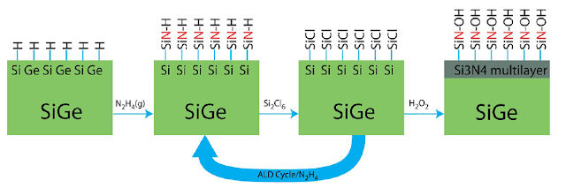
A low Temperature Passivation on SiGe(110) via plasma free process by subsequent doses of anhydrous hydrazine and hexachlorodisilane can further increase the amount of SiNx on the surface. A final treatment with HOOH can prepare the surface for high-k deposition.

BRUTE Peroxide was reported to reduce HfO2 gate oxide EOT by reduction in the interface layer

Steve Consiglio from Tokyo Electron, presented data comparing growth of HfO2 and interface layer thickness control [3]. Utilizing 300 mm Si wafers with pre-formed chemical oxide, he evaluated an all in-situ method of chemical oxide removal (COR; Si-H termination) followed by H2O2(g) dosing prior to ALD growth of HfO2 using TEMAHf and H2O. The study reported faster growth rate with H2O2 than for O3. Most interestingly, the interface results were very exciting with interface layer regrowth in the 2-4 Ångstrom range, which corresponds to ½ to 1 monolayer of SiOx interface for improved EOT and this was definitely much thinner than the results reported using O3.
Aluminum oxide, Al2O3 ALD has been presented previously [4]. This time RASIRC had a poster on improved nucleation by using H2O2 as an oxidant in ALD of Al2O3 [5]. The poster explained the need for a novel oxidant that improves passivation and nucleation density at semiconductor interfaces. The study was performed on SiGe(110) surfaces and  provides a direct comparison of equal amounts of water, 30% H2O2/H2O, and anhydrous H2O2. A five-fold increase was found in nucleation density for H2O2 versus water, and a three-fold increase for H2O2 versus 30% H2O2/H2O. An additional comparison was made of H2O2 to H2O by deposition of Al2O3 on an Si-H surface. This comparison found denser nucleation and faster initiation for H2O2 treated surfaces.
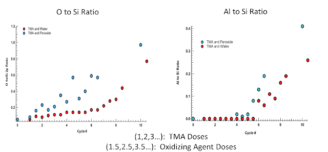


In a direct comparison of TMA based ALD with water vs peroxide the coverages of O and Al are higher with peroxide and growth starts earlier.

Zirconium oxide, ZrO2  was presented in study by Intermolecular and RASIRC at ALD2016 Poster session [6]. By utilizing the Intermolecular Combinatorial ALD platform equipped with a RASIRC BRUTE H2O2 apparatus the study compared the performance of H2O2 against O3 in a zirconium oxide ALD using ZyALD Air Liquide industry standard Zr-precursor. By MIMCAP integration the differences in ZrOx unit film properties and electrical performance was shown. Similar unit film behavior (GPC, linearity, growth saturation, film crystallinity etc.) was observed between O3 and H2O2.


Oxidant dosing (left) show that 4% O3 yields saturated response, whereas H2O2 and 20% O3 display softer saturation. ZyALD dose (middle) for each oxidant system shows definite completion for 20% O3. All three investigated conditions show linear growth without growth inhibition (right).       


The MIMCAP study (above) concluded that ZrO2 produced with H2O2 matched the best performance of 4% O3. Therefore it is possible to avoid issues observed with high (20%) O3 concentration as showcased in the figure below. More importantly, H2O2 has the capability to produce thin node dielectric, which is needed for highly scaled DRAM nodes.

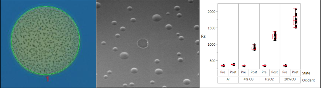
Optical (left) and SEM (middle) images of MIMCAPs, post-annealing, with defects observed with 20% O3 and thin 5 nm ZrOx. As comparison blanket TiN film enhanced resistivity was observed (right) using 4 resp. 20% O3 concentrations, whereas H2O2 lays in-between. Results suggest that elevated TiN bottom electrode oxidation takes place with 20% O3 that leads to degassing during annealing.  However, the defect can be avoided with minimal reduction in growth rate, by using H2O2 as the oxidant.
Hafnium oxide, HfO2 by TDMAHf along TEMAHf was the first Hf-precursors in use at the introduction of High-k in the DRAM industry more than 10 years ago at the 90nm node. HfO2 ALD has also been investigated by Intermolecular using the H2O2/TDMAHf ALD process and in this study the MIMCAPs showed to match the best O3 performance like in the case of ZrO2 given in more detail above. In addition, Tokyo Electron presented work for HfO2 as summarized above.  
Titanium oxide, TiO2 low temperature (100 °C) TiOx ALD using H2O2 and TiMCTA (methylcyclopentadienyl tris(dimethylamino)titanium) as the metal precursor has successfully been grown as also reported by Intermolecular at ALD2016 Poster session [6].  
   
To summarize, RASIRC and their collaborations throughout the semiconductor insdustry and with leading research facilities have shown that many different films can be grown with BRUTE Peroxide and BRUTE Hydrazine and most importantly that BRUTE Peroxide can reduce EOT by reduction in the interface layer, yielding higher performing memory and logic devices.
References
[1] D. R. Lide, CRC Handbook of Chemistry and Physics (CRC Press, Boca Raton, 1996).
[2] Hydrogen peroxide gas for improved nucleation and initiation in ALD, Daniel Alvarez, Adam Hinckley, Pablo Macheno, Christopher Ramos, Jeffrey Spiegelman,
Anthony Muscat, Presentation at ALD 2016 Ireland.
[3] Anhydrous H2O2 for ALD HfO2 growth and interfacial layer thickness control, Steven Consiglio, Robert Clark, Takahiro Hakamata, Kandabara Tapily, Cory Wajda, Gert Leusink, Presentation at ALD2016 Ireland.
[4] Comparison of Water Vapor to Ozone for Growth ALD Films, J. Spiegelman, J. Sundqvist, EU PVSEC Proceedings 2011, page 1694 – 1698.
[5] Hydrogen peroxide gas for improved nucleation and initiation in ALD, Daniel Alvarez, Adam Hinckley, Pablo Macheno, Christopher Ramos, Jeffrey Spiegelman, Anthony Muscat, Poster ALD2016 Ireland.
[6] Comparison of hydrogen peroxide and ozone for use in zirconium oxide atomic layer deposition, Gregory  Nowling,  Stephen Weeks, Daniel Alvarez, Mark Leo, Jeff Spiegelman, Karl Littau, Poster ALD2016 Ireland.