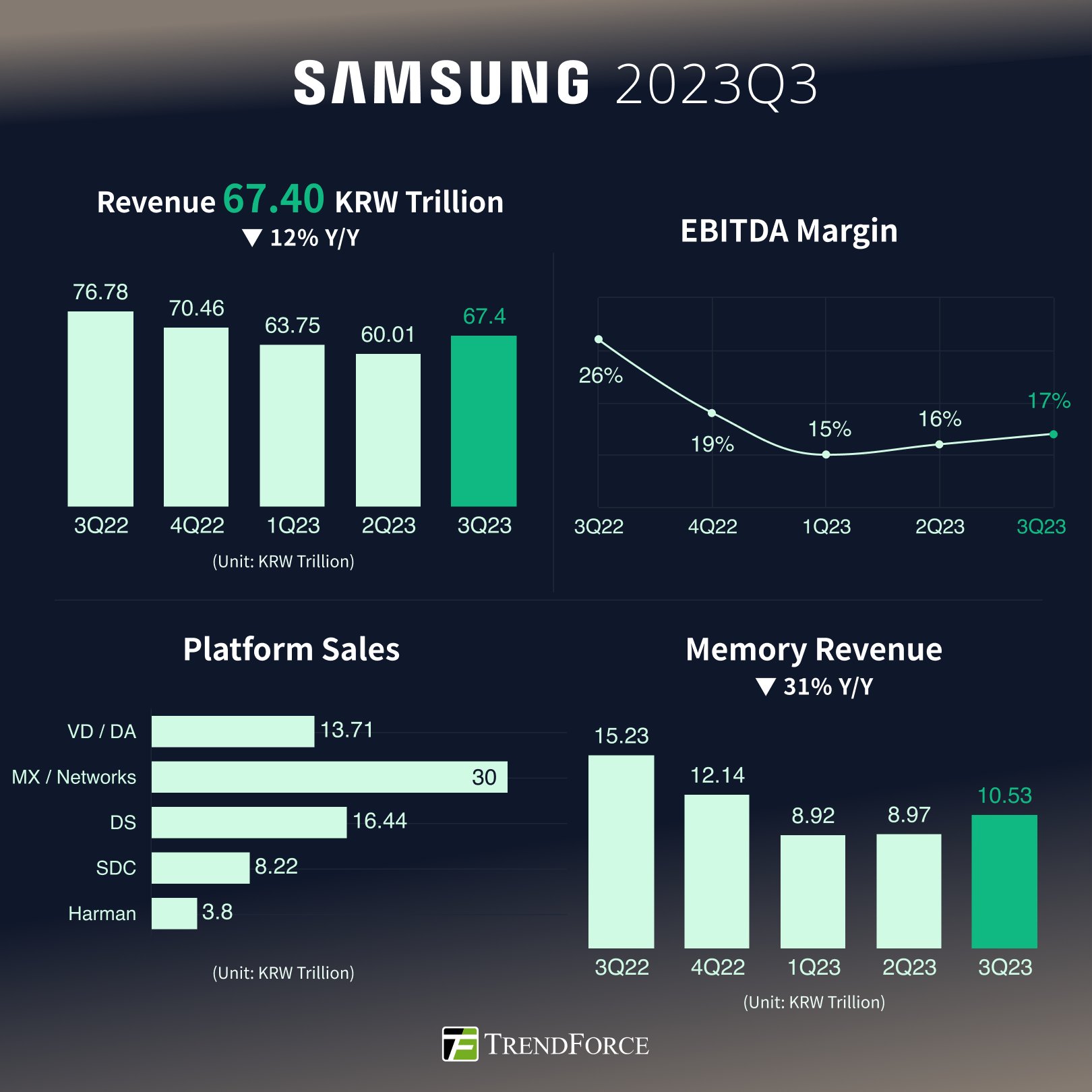
Showing posts with label DRAM. Show all posts

Wednesday, November 1, 2023

Surge in HBM Demand Marks Memory Market Recovery and Anticipated Growth in 2024 for Samsung

The global memory market, after experiencing a period of stagnation, has witnessed a resurgence in the third quarter, driven primarily by increased demand for high-density DRAM and NAND products in the PC and mobile sectors.

Samsung Electronics' financial results for 3Q23 highlighted a 12% QoQ revenue increase to 67.40 trillion Korean won, although there was a 12% YoY decrease. Notably, the company reported its highest quarterly profit for the year. Despite potential economic uncertainties in 2024, Samsung is optimistic about the recovery of the memory market and the rebound in smartphone demand. 

The memory sector saw a recovery compared to the previous quarter, especially in PC and mobile due to the rise in adoption of high-density DRAM and NAND products. The completion of customer inventory adjustments also played a role. Server demand was subdued for traditional servers due to macroeconomic uncertainties. However, strong demand persisted for AI-oriented high-density products. Samsung emphasized its focus on expanding sales of advanced node products like HBM DDR5, LPDDR5, and UFS 4.0. They also intend to manage high inventory products through production adjustments. The company expects the recovery trend in the memory market to accelerate further in the fourth quarter. Additionally, there has been a notable surge in HBM demand and the company is actively advancing its HBM businesses and plans to augment its HBM supply capacity by 2.5 times next year.


Trendforce on X (LINK)

The foundry division secured a record number of new orders, particularly in the HPC domain, despite a slow recovery in the mobile market. The new Taylor factory in Texas is set to begin production using the second-gen 3nm GAA process. The advanced packaging business has also been flourishing with orders from both domestic and international HPC clients.

Profits in the mobile panel business surged due to new flagship models from major clients. In contrast, the large panel business faced tepid demand. Samsung aims to cater to the growing mobile panel demand and increase profitability in the large panel sector by introducing new products and enhancing yield rates.

With the global economy expected to bounce back in 2024, the smartphone market's demand is anticipated to surge. High-end market growth is likely to continue, driven by the global recovery of the smartphone market.

Looking ahead to 2024, Samsung anticipates increased PC and mobile demand due to product replacement cycles initiated during the pandemic's early phase. High-density trends in both DRAM and NAND are expected to persist, propelled by on-device AI advancements. The company plans to focus on advanced node products, including 1B nanometer DDR5, LPDR5X, PCI Gen 5, and UFS 4.0, to bolster product competitiveness and profitability. Emphasizing the growing demand for generative AI, Samsung aims to strengthen its market position with high-density, low-power, and high-performance products for on-device AI, which has recently gained significant attention.

Sources;

TrendForce on X: "Samsung Electronics has released its financial results for 3Q23, reporting a quarterly revenue of 67.40 trillion Korean won—a 12% QoQ increase but 12% YoY decrease. The company achieved its highest quarterly profit of the year and anticipates that, despite ongoing global economic… https://t.co/RDKVjimgzN" / X (twitter.com)

Samsung Electronics Co Ltd (SSNLF) Q3 2023 Earnings Conference Call Transcript | Seeking Alpha


Tuesday, October 31, 2023

Micron's Distinct Approach to DRAM and Apple Design Wins

The tech landscape has seen consistent advancements, especially with the D1β (D1b) DRAM generation. Micron's D1β LPDDR5 16 Gb DRAM chips, integrated into the Apple iPhone 15 Pro, represent a significant step forward. Codenamed Y52P die, this chip offers an improved form factor and density, especially when contrasted with its LPDDR5/5X D1α 16 Gb predecessor. The integration of these chips into Apple's flagship device marks a significant design win for Micron, emphasizing the trust and partnership between the two tech giants.

In a recent teardown of the Apple iPhone 15 Pro, TechInsights has discovered a remarkable find - Micron's cutting-edge D1β LPDDR5 DRAM chips. These chips mark the industry's first foray into the D1β generation, and they are nothing short of impressive. (LINK)

Micron's technological direction is unique, especially with their decision to forego the Extreme Ultraviolet Lithography (EUVL) process, common in sub-15nm DRAM scaling. This stands in contrast to industry giants like Samsung and SK Hynix, who employ EUVL in their DRAM fabrication. Despite this, Micron has successfully launched the D1z, D1α, and D1β DRAM chips without EUVL, illustrating an alternative yet effective DRAM scaling approach.


In wrapping up, while Samsung and SK Hynix utilize EUVL in their DRAM processes, Micron has carved a different path, further solidified by their design wins with Apple. This partnership not only underscores Micron's technological prowess but also indicates the potential of varied methodologies in shaping the future of DRAM technology.


Source: Micron's D1β LPDDR5 Chip: Great Advancements in Memory Technology | Semiconductor Materials and Equipment (abachy.com)

Wednesday, October 18, 2023

Micron Unveils Breakthrough NVDRAM: A Dual-Layer 32Gbit Non-Volatile Ferroelectric Memory with Near-DRAM Performance

At the upcoming International Electron Devices Meeting (IEDM), Micron is set to present a paper on a novel 32Gbit non-volatile ferroelectric memory, termed NVDRAM. Authored by Nirmal Ramaswamy, the vice president of advanced DRAM and emerging memory at Micron, the paper is titled "NVDRAm: A 32Gbit Dual Layer 3D Stacked Non-Volatile Ferroelectric Memory with Near-DRAM Performance for Demanding AI Workloads". It introduces the world’s first dual-layer, high-performance, 32Gbit stackable ferroelectric memory technology. This technology, branded as non-volatile dynamic random access memory (NVDRAM), promises faster data movement and better energy efficiency than traditional DRAM, making it ideal for larger neural network models.

NVDRAM merges the benefits of ferroelectric memory cells – non-volatility and high endurance – with performance surpassing NAND flash memory retention and offering DRAM-like read/write speeds. The memory's architecture uses a 5.7nm ferroelectric capacitor for charge retention in a 1T1C DRAM structure, while dual-gated polycrystalline silicon transistors control access. The stacked double memory layer resides above a CMOS access circuit layer on a 48nm pitch. Despite the technological advancements, commercialization discussions remain speculative, potentially awaiting feedback from the IEDM presentation.


The images above show the final die layout (left) and SEM cross-section (center) of a 32Gb NVDRAM with 1T1C memory layers, fabricated over a CMOS array. On the right is a schematic diagram of NVDRAM memory arrays, showing polysilicon access device with orthogonal wordline (WL) and digitline (DL), and ferroelectric memory cells.

Abstract: Non-Volatile Ferroelectric w/DRAM-Like Performance, for AI & Machine Learning: Rapid growth in the size of the data models used in artificial intelligence (AI) and machine-learning (ML) applications is creating an urgent need for higher-bandwidth memory solutions. While new compute paradigms like near-memory-compute and processing-in-memory are being investigated, the best near-term opportunity is to outfit existing, traditional compute architectures with more efficient memory for faster data movement and to accommodate larger models. In this year’s Generative AI Focus Session, Micron researchers will unveil a memory technology for these uses which they call NVDRAM. It is the world’s first dual-layer, high-performance, high-density (32Gb), stackable and nonvolatile ferroelectric memory technology. It combines the non-volatile, high-endurance nature of ferroelectric memory cells with DRAM-like read/write speeds and endurance, and also surpasses the retention performance of NAND memory. NVDRAM uses an ultra-scaled (5.7nm) ferroelectric capacitor as the memory cell, and a dual-gated, stackable, polycrystalline silicon transistor as the access device. To achieve high memory density, two memory layers are fabricated above CMOS circuitry in a 48nm pitch, 4F2 architecture. Full package yield is demonstrated from -40°C to 95°C, along with reliability of 10 years (for both endurance and retention).

Sources:

Tuesday, September 26, 2023

TechInsights Discovers Micron's Cutting-Edge D1β LPDDR5 16 Gb DRAM Chips in Apple iPhone 15 Pro: Setting a New Standard in Memory Technology

TechInsights has confirmed Micron's cutting-edge D1β LPDDR5 16 Gb DRAM chips in the Apple iPhone 15 Pro, marking the industry's first venture into the D1β generation. These chips are smaller and denser than their predecessors, showcasing significant advancements in DRAM technology. Notably, Micron has achieved this without utilizing Extreme Ultraviolet Lithography (EUVL), a technique employed by competitors like Samsung and SK Hynix for their DRAM processes. This achievement highlights Micron's dedication to pushing the boundaries of DRAM technology, emphasizing innovation and efficiency in the tech landscape. Micron's groundbreaking D1β LPDDR5 16 Gb DRAM chip promises to reshape the future of memory technology, setting a new standard for the industry.

(Source Micron.com)

1-BETA includes cool stuff

High-k/Metal Gate

Micron's 1β fabrication process uses the company's 2nd generation high-K metal gate (HKMG) and is said to increase bit density of a 16Gb memory die by 35% as well as to improve power efficiency by 15% when compared to a similar DRAM device made on the company's 1α node

Pitch multiplication without the need for EUV Lithography

Micron's use of proprietary multi-patterning lithography involves advanced techniques for defining circuit patterns on semiconductor wafers with the highest precision. This approach allows Micron to create intricate patterns on the chips, achieving higher memory capacity in a smaller footprint. It enables the company to fit billions of memory cells on a chip that's roughly the size of a fingernail. 

While the semiconductor industry has been transitioning to extreme ultraviolet lithography (EUVL) to overcome technical challenges in patterning, Micron has opted for its multi-patterning lithography approach. This choice showcases Micron's expertise and innovation in lithography techniques, enabling them to continue shrinking circuit features and achieving greater memory capacity without relying on EUVL, which is still considered an emergent technology. 

By using proprietary multi-patterning lithography, Micron not only reduces the cost per bit of data but also enables devices with small form factors, such as smartphones and IoT devices, to incorporate more memory into compact spaces. This approach underscores Micron's commitment to staying at the forefront of memory technology innovation.
"While the industry has begun to shift to a new tool that uses extreme ultraviolet light to overcome these technical challenges, Micron has tapped into its proven leading-edge nano-manufacturing and lithography prowess to bypass this still emergent technology. Doing so involves applying the company’s proprietary, advanced multi-patterning techniques and immersion capabilities to pattern these minuscule features with the highest precision," Micron explains. Thy Tran, VP Process Integration, Micron


On the heels of the news that Micron has begun shipping QS-sample LPDDR5X components developed on the new 1-beta DRAM process node to its smartphone customers, host Jim Greene welcomes Thy Tran, Vice President of DRAM Process Integration, to the Chips Out Loud Podcast to discuss the emergent technology.

Sources:

Micron LPDDR5 16 Gb Non-EUVL Chip Found in Apple iPhone 15 Pro | TechInsights

LPDRAM | LPDDR | Micron Technology

Micron Ships World’s Most Advanced DRAM Technology With 1-Beta Node | Micron Technology


(Source: TechInsights.com)


Monday, September 25, 2023

NEO Semiconductor Unveils Revolutionary 3D NAND and DRAM Innovations at Flash Memory Summit 2023

NEO Semiconductor, known for its expertise in 3D NAND flash and DRAM technologies, presented groundbreaking innovations at Flash Memory Summit 2023 in August. The full presentation can be seen on Youtube (below). CEO Andy Hsu's keynote introduced their latest creation, 3D X-DRAM™, designed to overcome DRAM's capacity limitations and replace 2D DRAM. This technology utilizes the existing 3D NAND flash process with minor modifications, streamlining development and reducing costs. Hsu also unveiled a new AI application, "Local Computing," promising a substantial enhancement in AI chip performance.


X-DRAM™ significantly reduces data latency and provides ultra-high data throughput to unleash the full potential of High-Bandwidth Memory (HBM). HBM uses many Through Silicon Via (TSV) to increase I/O bandwidth. However, the HBM data latency remains almost the same when using conventional DRAM because bit line lengths remain the same.

Furthermore, NEO Semiconductor showcased various novel memory structures derived from 3D X-DRAM™, tailored for applications like 3D NOR flash memory, 3D Ferroelectric RAM (FFRAM), 3D Resistive RAM (RRAM), 3D Magnetoresistive RAM (MRAM), and 3D Phase Change Memory (PCM). These innovations enable the transition from 2D to 3D memory cells.


Hsu underscored the significance of these technologies for the semiconductor industry, cloud providers, and enterprises, highlighting that 3D X-DRAM™ offers a high-speed, high-density, cost-effective, and high-yield solution.

The presentation addressed the challenges faced by DRAM and NAND flash memory in the context of AI applications and introduced two innovative solutions – 3D X-DRAM™ and 3D X-NAND™.

Being part of the prestigious Flash Memory Summit, NEO Semiconductor showcased its technologies at booth number 215, and interested parties had the opportunity to schedule meetings with the company at the event.

In summary, NEO Semiconductor unveiled groundbreaking advancements in 3D NAND flash and DRAM technologies at Flash Memory Summit 2023, offering solutions to critical challenges in memory performance and capacity.

Source: NEO Semiconductor to Present Its Ground-Breaking 3D NAND and 3D DRAM Architectures in Keynote Address at Flash Memory Summit 2023 - Neo Semiconductor | X-Nand


Tuesday, September 5, 2023

"Micron to Produce Advanced Memory Chips in Taiwan Using EUV Lithography by 2025, Reinforces Commitment to Island's Semiconductor Industry"

Micron Technology is set to begin producing memory chips in Taiwan using advanced EUV lithography technology by 2025, ahead of its other production sites. The company's local division head, Donghui Lu, confirmed this move and emphasized that Taiwan remains a top investment destination for Micron. The collaboration with Japanese and Taiwanese companies facilitated the development of this technology. 

Micron's decision to produce HBM type memory in Taiwan highlights the island's significance in its operations, accounting for up to 65% of production volumes. The advantageous Taiwanese infrastructure and the company's commitment to geographic diversification contribute to its expanding and modernizing operations. This move underscores Micron's dedication to innovation and maintaining a competitive edge in the semiconductor industry.

Source: Aroged: Micron will begin producing memory in Taiwan using EUV lithography by 2025 - Aroged


Saturday, August 26, 2023

SK Hynix Leads DRAM Industry's Rebound in Q2 with Revenue Surge, Reclaims No. 2 Position

South Korea's SK Hynix Inc. has orchestrated a substantial resurgence in the DRAM chip sector during Q2, propelling itself back to the second-largest global position and surging ahead of Micron Technology Inc., which now stands third. The chipmaker achieved a nearly 50% surge in DRAM shipments, propelling its revenue to $3.44 billion in the April-June period. Notably, SK Hynix excelled in DDR5 and HBM chip shipments, products with higher average selling prices (ASPs) than standard commodity DRAM items, thus enhancing its ASP growth by 7-9% compared to the previous quarter. In contrast, market leader Samsung Electronics experienced a 7-9% ASP drop while retaining its top position, and third-place Micron sustained relatively stable ASP with DDR5 shipments. The overall DRAM industry marked a 20.4% QoQ revenue increase in Q2, signaling a potential turnaround in the sector.

SK Hynix leads DRAM industry’s Q2 revenue rebound, retakes No. 2 spot - KED Global

Tuesday, May 2, 2023

TechInsights found Samsung DRAM chips in Samsung Galaxy S23 with Five EUV mask layers

TechInsights found Samsung DRAM chips in Samsung Galaxy S23 with Five EUV mask layers. These are from DRAM wafers produced in the so-called D1a node (or D1α, α as in alpha)


This is in line with a previous press release from Samsung (2020) so no real surprise here: Samsung Announces Industry’s First EUV DRAM with Shipment of First Million Modules – Samsung Global Newsroom

"EUV to be fully deployed from 4th-gen 10nm-class DRAM (D1a) next year"

EUV will be fully deployed in Samsung’s future generations of DRAM, starting with its fourth-generation 10nm-class (D1a) or the highly-advanced 14nm-class, DRAM. Samsung expects to begin volume production of D1a-based DDR5 and LPDDR5 next year, which would double manufacturing productivity of the 12-inch D1x wafers.


Tuesday, February 8, 2022

Samsung Electronics Is Pushing Hard to Bring Monolithic 3D DRAM to HVM by 2025

Samsung Electronics has been enjoying its DRAM market leader position for about 30 years now. To retain the position further, it has intensified its R&D of monolithic 3D DRAMs to bring them to HVM by 2025.


DRAM’s performance boost based on scaling the cell size or pitch is approaching a physical limit for cramming more cells in a limited space. Additionally, the ultra-high aspect ratio capacitors may collapse leading to compromised device reliability. Therefore, switching from current 2D DRAMs to next-generation monolithic 3D DRAMs seems inevitable.

Samsung has reportedly intensified its R&D on stacking DRAM cells on top of each other in a monolithic fashion, unlike in the case of high-bandwidth memory (HBM), wherein multiple dies are stacked atop each other.

Besides High-k/Metal Gate transistor technology, Samsung is also considering adopting FinFET or gate-all-around (GAA) technology for the DRAM cell transistor to attain better electrostatic control of the charge flow within the channel with the gate electrode.

Micron Technology and SK Hynix are also reportedly developing monolithic 3D DRAMs. Micron recently filed a patent for a monolithic 3D DRAM that is different from that of Samsung. Micron’s approach is to change the shapes of the transistor and capacitor without laying down a cell. Major equipment manufacturers such as Applied Materials and Lam Research are also developing solutions for the monolithic 3D DRAMs.

By Abhishek Kumar Thakur & Jonas Sundqvist

Friday, May 7, 2021

Applied Materials MEMORY MASTER CLASS 2021 - slide deck

I missed this opportunity, however, I am grateful for Lita Shon-Roy just sending me the link to the slide deck - Tack så mycket. 

Slide deck for the Memory Class LINK

Next class up is Logic June 16, 2021 followed by more interesting topics in 2nd half 2021:

  • Specialty semiconductors
  • Heterogeneous design and advanced packaging
  • Inspection and process control

Teaser slide (Credit Dr. Sony Varghese, Director of Strategic Marketing at at Applied Materials)

You are welcome to contact us at TECHCET (jsundqvist@techcet.com) to dig further into the future surge of materials to realize the data-driven economy:

  • ALD/CVD precursors
  • Metals/PVD Targets
  • Photoresist
  • Wet chemicals
  • CMP pads & slurries
  • Bulk, Rare and Speciality gases
  • Wafers

Applied Materials Introduces Materials Engineering Solutions for DRAM Scaling

  • New Draco™ hard mask material co-optimized with Sym3® Y etcher to accelerate DRAM capacitor scaling
  • DRAM makers adopting Black Diamond®, the low-k dielectric material pioneered by Applied Materials to overcome interconnect scaling challenges in logic
  • High-k metal gate transistors now being introduced in advanced DRAM designs to boost performance and reduce power while shrinking the periphery logic to improve area and cost
SANTA CLARA, Calif., May 05, 2021 (GLOBE NEWSWIRE) -- Applied Materials, Inc. today announced materials engineering solutions that give its memory customers three new ways to further scale DRAM and accelerate improvements in chip performance, power, area, cost and time to market (PPACt).
The Draco hard mask resolves this issue with a new material whose selectivity is more than 30 percent higher than conventional DRAM capacitor hard masks. It enables the deposition of a 30 percent thinner hard mask, thus decreasing the capacitor’s aspect ratio and easing the difficulty of the etch process.

The digital transformation of the global economy is generating record demand for DRAM. The Internet of Things is creating hundreds of billions of new computing devices at the edge which are driving an exponential increase in data transmitted to the cloud for processing. The industry urgently needs breakthroughs that can allow DRAM to scale to reduce area and cost while also operating at higher speeds and using less power.
Applied Materials is working with DRAM customers to commercialize three materials engineering solutions that create new ways to shrink as well as improve performance and power. The solutions target three areas of DRAM chips: storage capacitors, interconnect wiring and logic transistors. They are now ramping into high volume and are expected to significantly increase Applied’s DRAM revenue over the next several years.

Introducing Draco™ Hard Mask for Capacitor Scaling

Since over 55 percent of a DRAM chip’s die area is occupied by the memory arrays, increasing the density of these cells is the biggest lever for reducing cost per bit. Data is stored as charges in cylindrical, vertically arranged capacitors that need as much surface area as possible to hold adequate numbers of electrons. As DRAM makers narrow the capacitors, they also elongate them to maximize surface area. A new technology challenge to DRAM scaling has emerged: the etching of the deep capacitor holes threatens to exceed the limits of the “hard mask” material that acts as a stencil to determine where each cylinder is placed. If the hard mask is etched through, the pattern is ruined. Taller hard masks are not viable because as the combined depth of the hard masks and capacitor holes exceeds certain limits, etch byproducts remain and cause bending, twisting and uneven depths.


Applied Producer® XP Precision® Draco™ CVD

The solution is Draco™, a new hard mask material that has been co-optimized to work with Applied’s Sym3® Y etch system in a process monitored by Applied’s PROVision® eBeam metrology and inspection system that can take nearly half a million measurements per hour. The Draco hard mask increases etch selectivity by more than 30 percent which enables a shorter mask. Draco hard mask and Sym3 Y co-optimization includes advanced RF pulsing which synchronizes etching with byproduct removal to enable patterning holes that are perfectly cylindrical, straight and uniform. The PROVision eBeam system gives customers massive, immediate actionable data on hard mask critical dimension uniformity which is the key to capacitor uniformity. Applied’s solution provides customers with a 50-percent improvement in local critical dimension uniformity and reduces bridge defects by 100X, thus increasing yields.


Implementation of Draco for DRAM capacitors. (Applied Materials Master Memory Class May the 5th 2021 LINK)

“The best way to quickly solve materials engineering challenges with our customers is to co-optimize adjacent steps and use massive measurements and AI to optimize process variables,” said Dr. Raman Achutharaman, group vice president, Semiconductor Products Group at Applied Materials.


Bringing Black Diamond® Low-k Dielectric to the DRAM Market

A second key lever of DRAM scaling is reducing the die area needed by the interconnect wiring that routes signals to and from the memory arrays. Each of the metal lines is surrounded by an insulating dielectric material to prevent interference between data signals. For the past 25 years, DRAM makers have used one of two silicon oxides – silane and tetraethoxysilane (TEOS) – as the dielectric material. Continual thinning of the dielectric layers has reduced DRAM die sizes but created a new technology challenge: the dielectrics are now too thin to prevent capacitive coupling in the metal lines whereby signals interfere with one another causing higher power consumption, slower performance, increased heat and reliability risks.

The solution is Black Diamond®, a low-k dielectric material first used in advanced logic. With DRAM designs now experiencing similar scaling challenges, Applied is adapting Black Diamond to the DRAM market and making it available on the highly productive Producer® GT platform. Black Diamond for DRAM enables smaller, more compact interconnect wires that can move signals through the chips at multi-gigahertz speeds without interference and at lower power consumption.

High-k Metal Gate Transistors Bring PPAC Improvements to DRAM

A third key lever of DRAM scaling is improving the performance, power, area and cost of the transistors used in the periphery logic of the chip to help drive the input-output (I/O) operations needed in high-performance DRAM like those based on the new DDR5 specification.

Until today, DRAM used transistors based on polysilicon-oxide which were phased out in foundry-logic by the 28-nanometer node because extreme thinning of the gate dielectric allowed electrons to leak, thereby wasting power and limiting performance. Logic makers adopted high-k metal gate (HKMG) transistors, replacing the polysilicon with a metal gate and the dielectric with hafnium oxide, a material that improves gate capacitance, leakage and performance. Now memory makers are designing HKMG transistors into advanced DRAM designs to improve performance, power, area and cost. In DRAM as in logic, HKMG will increasingly replace polysilicon transistors over time.

This technology inflection in DRAM creates growth opportunities for Applied Materials. The more complex and delicate HKMG materials stack is challenging to manufacture, and in-vacuum processing of adjacent steps using Applied’s Endura® Avenir™ RFPVD system has become the industry’s preferred solution. HKMG transistors also benefit from Applied’s epitaxial deposition technologies such as Centura® RP Epi along with film treatments including RadOx™ RTP, Radiance® RTP and DPN which are used to fine-tune the transistor characteristics for optimum performance.

“Draco hard mask and Black Diamond low-k dielectric are being adopted by leading DRAM customers, and the first HKMG DRAMs are now being introduced,” added Dr. Achutharaman. “Applied Materials projects billions of dollars in revenue growth as these DRAM inflections play out over the next several years.”

Additional information about the growth outlook for these technologies is being provided at Applied’s 2021 Memory Master Class being held later today. For more information, please visit the investor page of our website at https://ir.appliedmaterials.com.

Friday, March 26, 2021

Samsung confirms first HKMG for DDR5 DRAM

ASM International recently acknowledged that ALD High-k/Metal Gate (HKMG) is finally in high volume production for DRAM (LINK). Now Samsung confirms that. This is a small victory for all people working on this process for such a long time. My first tool ownership when I moved to Germany and started at Infineon was an ASM Polygon 200 mm cluster with a Pulsar 2000 chamber running HfO2, TiN, TiHfN, TiAlN, Al2O3, and my not fully understood HfN ALD process and a Poly chamber that I never really cared too much about. Press release below - and now do the maths - how big this business is once rolled out for all DRAM technologies to come - yeah $$$, many tulips indeed.


Samsung Develops Industry’s First HKMG-Based DDR5 Memory; Ideal for Bandwidth-Intensive Advanced Computing Applications

512GB capacity DDR5 module made possible by an 8-layer TSV structure
HKMG material reduces power by 13 percent while doubling the speed of DDR4


Samsung Electronics, the world leader in advanced memory technology, today announced that it has expanded its DDR5 DRAM memory portfolio with the industry’s first 512GB DDR5 module based on High-K Metal Gate (HKMG) process technology. Delivering more than twice the performance of DDR4 at up to 7,200 megabits per second (Mbps), the new DDR5 will be capable of orchestrating the most extreme compute-hungry, high-bandwidth workloads in supercomputing, artificial intelligence (AI) and machine learning (ML), as well as data analytics applications.


“Samsung is the only semiconductor company with logic and memory capabilities and the expertise to incorporate HKMG cutting-edge logic technology into memory product development,” said Young-Soo Sohn, Vice President of the DRAM Memory Planning/Enabling Group at Samsung Electronics. “By bringing this type of process innovation to DRAM manufacturing, we are able to offer our customers high-performance, yet energy-efficient memory solutions to power the computers needed for medical research, financial markets, autonomous driving, smart cities and beyond.”

“As the amount of data to be moved, stored and processed increases exponentially, the transition to DDR5 comes at a critical inflection point for cloud datacenters, networks and edge deployments,” said Carolyn Duran, Vice President and GM of Memory and IO Technology at Intel. “Intel’s engineering teams closely partner with memory leaders like Samsung to deliver fast, power-efficient DDR5 memory that is performance-optimized and compatible with our upcoming Intel Xeon Scalable processors, code-named Sapphire Rapids.”

Samsung’s DDR5 will utilize highly advanced HKMG technology that has been traditionally used in logic semiconductors. With continued scaling down of DRAM structures, the insulation layer has thinned, leading to a higher leakage current. By replacing the insulator with HKMG material, Samsung’s DDR5 will be able to reduce the leakage and reach new heights in performance. This new memory will also use approximately 13% less power, making it especially suitable for datacenters where energy efficiency is becoming increasingly critical.

The HKMG process was adopted in Samsung’s GDDR6 memory in 2018 for the first time in the industry. By expanding its use in DDR5, Samsung is further solidifying its leadership in next-generation DRAM technology.

Leveraging through-silicon via (TSV) technology, Samsung’s DDR5 stacks eight layers of 16Gb DRAM chips to offer the largest capacity of 512GB. TSV was first utilized in DRAM in 2014 when Samsung introduced server modules with capacities up to 256GB.

Samsung is currently sampling different variations of its DDR5 memory product family to customers for verification and, ultimately, certification with their leading-edge products to accelerate AI/ML, exascale computing, analytics, networking, and other data-intensive workloads


Friday, February 26, 2021

Tech Insights Teardown: Samsung’s D1z DRAM with EUV Lithography

Advanced and costly schemes for ArFi immersion-based multi-pattering are definitely running out of steam for leading-edge logic and EUV is continuing the march into high volume manufacturing now also for DRAM. The other day there was an announcement that SK Hynix, the world´s number two DRAM maker has signed a 5-year agreement with ASML for EUV scanners (LINK).

As a European, I must say that I like the situation that the key to continued scaling is kept in The Netherlands (ASML) and also the important key technology providers in Germany (Zeiss SMT, Trumpf) and Belgium in the form of the worlds leading research institute for scaling CMOS - imec and the EUV Resist Manufacturing & Qualification Center NV (EUV RMQC), a Joint Venture between imec and  JSR Micro NV (LINK).

Reuters: SK Hynix signs five-year deal worth $4.3 billion with ASML to secure EUV scanners


Now DRAMs from Samsung Electronics with applied EUV lithography technology for D1z DRAM in mass production have been found in the field and analyzed by Tech Insights and reported by EETimes (LINK).

According to EETimes, Samsung Electronics announced the world’s first development of both ArF-i based D1z DRAM and separately its EUV lithography (EUVL) applied D1z DRAM last year.

Tech Insights is excited that we have finally found Samsung’s new and advanced D1z DRAM devices and confirmed details of this technology.

Here just a teaser, please check out the original EETimes article or get the full report from Tech Insights (LINK).


Samsung DRAM cell design, a comparison of BLP patterns on D1z (a) without EUVL and (b) with EUVL.


Tuesday, February 9, 2021

Capacitorless DRAM using oxide semiconductors could be built in 3D layers above a processor’s silicon

One of the biggest problems in computing today is the “memory wall”—the difference between processing time and the time it takes to shuttle data over to the processor from separate DRAM memory chips. The increasingly popularity of AI applications has only made that problem more pronounced, because the huge networks that find faces, understand speech, and recommend consumer goods rarely fit in a processor’s on-board memory.

In December at IEEE International Electron Device Meeting (IEDM), separate research groups in the United States and in Belgium think a new kind of DRAM might be the solution. The new DRAM, made from oxide semiconductors and built in the layers above the processor, holds bits hundreds or thousands of times longer than commercial DRAM and could provide huge area and energy savings when running large neural nets, they say.


The transistors in the capacitorless DRAM developed by U.S.-based researchers includes a tungsten-doped indium oxide [orange] semiconductor, palladium top and bottom gates [yellow], nickel source and drain electrodes [green] and hafnium oxide dielectrics [blue]. Image: University of Notre Dame

Thursday, January 28, 2021

Micron Delivers Industry’s First 1α DRAM Technology

Micron recently announced that they are shipping memory chips built using the world’s most advanced DRAM process technology, which offers major improvements in bit density, power and performance. This is an astonishing feat of nanofabrication. 

Micron announcement: Micron Delivers Industry’s First 1α DRAM Technology

Micron’s 1α DRAM node will facilitate more power-efficient, reliable memory solutions and provide faster LPDDR5 operating speeds for mobile platforms that require best-in-class LPDRAM performance. Micron’s innovation brings the industry’s lowest-power mobile DRAM, with a 15% improvement in power savings,1 allowing 5G mobile users to perform more tasks on their smartphones without sacrificing battery life.

To find out more watch Thy Tran, vice president of DRAM Process Integration at Micron previously with Qimonda explain how to realize this amazing technology.


According to more details given in a Blog by Thy Tran, Micron uses Quadruple Patterning or Quad Patterning to realize the most critical lithography layers, which employ multiple ALD process steps and has become one of the biggest ALD market segment over recent years. See the video below by Lam Research for some more insights!


Quad patterning process flow (Image: Lam Research)


Friday, December 18, 2020

Imec demonstrate BEOL compatible architecture that paves the way to high-density 3D-DRAM memories

LEUVEN (Belgium), 15 December 2020 — This week, at the 2020 International Electron Devices Meeting, imec, a world-leading research and innovation hub in nanoelectronics and digital technologies, presents a novel dynamic random-access memory (DRAM) cell architecture that implements two indium-gallium-zinc-oxide thin-film transistors (IGZO-TFTs) and no storage capacitor. DRAM cells in this 2T0C (2 transistor 0 capacitor) configuration show a retention time longer than 400s for different cell dimensions – significantly reducing the memory’s refresh rate and power consumption. The ability to process IGZO-TFTs in the back-end-of-line (BEOL) reduces the cell’s footprint and opens the possibility of stacking individual cells. These breakthrough results pave the way towards low-power and high-density monolithic 3D-DRAM memories.

(image: Imec)

Scaling traditional 1T1C (one transistor one capacitor) DRAM memories beyond 32Gb die density faces two major challenges. First, difficulties in Si-based array transistor scaling make it challenging to maintain the required off-current and world line resistance with decreasing cell size. Second, 3D integration and scalability – the ultimate path towards high-density DRAM – is limited by the need for a storage capacitor. Imec presents a novel DRAM architecture that responds to both challenges, thereby offering a scaling path towards low-power high-density 3D-DRAM memories.

The new architecture implements two IGZO-TFTs – which are well known for their very low off-current – and no storage capacitor. In this 2T0C configuration, the parasitic capacitance of the read transistor serves as the storage element. Resulting DRAM cells exhibit a retention time >400s thanks to an extremely low (extracted) off-current of 3x10-19A/µm. These breakthrough results were obtained for optimized scaled IGZO transistors (with 45nm gate length) processed on 300mm wafers. Optimization was directed towards suppressing the impact of oxygen and hydrogen defects on both on-current and threshold voltage – one of the main challenges for developing IGZO-TFTs.

Gouri Sankar Kar, Program Director at imec: “Besides the long retention time, IGZO-TFT-based DRAM cells present a second major advantage over current DRAM technologies. Unlike Si, IGZO-TFT transistors can be fabricated at relatively low temperatures and are thus compatible with BEOL processing. This allows us to move the periphery of the DRAM memory cell under the memory array, which significantly reduces the footprint of the memory die. In addition, the BEOL processing opens routes towards stacking individual DRAM cells, hence enabling 3D-DRAM architectures. Our breakthrough solution will help tearing down the so-called memory wall, allowing DRAM memories to continue playing a crucial role in demanding applications such as cloud computing and artificial intelligence.”

Wednesday, October 28, 2020

TechInsights Webinar: ALD/ALE Process in Commercially Available Memory Devices

2018 saw memory product manufacturers Samsung, Hynix, Toshiba and Micron introducing 64- or 72- stacked layer 3D-NAND devices, and move into 1x generation DRAM devices.

This presentation will examine some of the different structures we have seen through the evolution of these technologies, in particular the latest 3D-NAND and DRAM parts. We will also look at several historical applications of ALD/ALE technology that have been observed through reverse engineering. We will highlight the importance of ALD/ALE process in advanced logic devices. In many cases, the technology could not have advanced without the implementation of ALD technology.

Information and registration: LINK


Tuesday, May 19, 2020

Hafnium, Zirconium: Australian Strategic Materials a step closer to completing commercial pilot plan

Recent semiconductor materials related trade issues between Japan and South Korea have led South Korea to secure alternative sourcing of photoresists and metals for their semiconductor industry. This includes essential minerals for hafnium and zirconium ALD precursors that are used in the manufacturing of DRAM and Foundry logic at SK Hynix and Samsung fabs.

Besides the tension with Japan, China's dominance in the supply of zirconium chemicals and materials has highlighted the additional risk in the critical materials supply change for its important semiconductor and high tech industries.

One such action has been setting up a pilot plant in South Korea for hafnium and zirconium metal in joint development with Australias Alkane and its subsidiary Australian Strategic Materials (ASM). The joint undertaking has now moved to the next phase for a commercial operation of a pilot plant as reported by Alkaine below.

Australian Strategic Materials a step closer to completing commercial pilot plan

Australian Strategic Materials (ASM), a wholly owned subsidiary of Alkane Resources is getting closer to completing the construction of a commercial pilot plant facility in South Korea that will enable critical metal oxides, including zirconium and hafnium, to be converted into metals in clean, carbon-free way.

As the Covid-19 pandemic continues to highlight weaknesses in critical minerals supply chains globally, ASM has confirmed in Alkane Resources' quarterly recently it has received interest in both potential future supply and partnership from a number of parties in South Korea and elsewhere. ...

Read more.


Read more about previous blog about the Alkane Dubbo project in New South Wales, Austrailia:

The Dubbo Project - The High-k mine in Dubbo, NSW Australia

Hafnium product breakthrough consolidates Dubbo Project business case

China’s water crisis stems the flow of zirconium and rare earths for global industries

Alkane Resources reports that zirconium oxychloride (ZOC) prices are up 40% since January 2017


Monday, April 20, 2020

Choppy Waters for Shipping $50B of Semiconductor Materials in 2020

Risky Sailing on the Global Supply-Chain Seas

San Diego, CA, Apr 17, 2020:TECHCET announces that:
 
• 2020 global material revenues in semiconductor manufacturing forecasted to decline by 3.0% year-over-year (YoY) despite growth in 1Q2020,
• Impact of COVID-19 pandemic on the global economy is creating choppy waters for shipping and supplying critical materials, as highlighted in recent Critical Materials Council (CMC) monthly meetings, and
• With a return of global economic growth by 2021, compound annual growth rate (CAGR) through 2025 is forecast at 3.5% as shown in the Figure (below).


“From our market research, materials suppliers are increasing production and sales to ensure safety-stock throughout the supply-chain in case there are further disruptions due to COVID-19 cases,” remarked Lita Shon-Roy, TECHCET President and CEO. “Even without further disruptions, we can already see leading economic indicators such as unemployment levels, metal prices and container shipping indices point toward a significant decline in global GDP.” This is supported by the International Monetary Fund’s (IMF’s) current outlook on 2020.

Currently, almost all chip fabs appear to be running at normal levels, with a few exceptions. During this difficult period, YMTC in Wuhan, China reportedly has maintained R&D and grown production of 3D-NAND chips. However, chip fabs in Malaysia report that the government required companies to request permission to continue operating at 50% staffing levels. One company in France had to temporarily reduce production due to their labor union insisting on temporary workforce reductions.

Significant value-added engineered materials including specialty gases, deposition precursors, wet chemicals, chemical-mechanical planarization (CMP) slurries & pads, silicon wafers, PVD/sputtering targets, and photoresists & ancillary materials for lithography are reporting healthy orders and in some cases will see better than expected revenues for 1Q2020 and April 2020. However, more than 60% of all materials are expected to be negatively impacted before year-end.

Overall demand for commodity materials, such as silane and phosphoric acid, is expected to decline YoY in 2020 by an average of 3% due to softening of the global economy. Average selling prices (ASP) for electronic-grade commodities may drop due to cost reductions in feed-stocks; for example, the global helium (He) gas market which had been forecasted to be in shortage with high ASPs throughout 2020 has already improved due to COVID-19 slowing down helium demand.

DRAM, 3D-NAND, and MPU chips for server / cloud-computing applications are now in high demand for virtual meetings and remote work. It is yet unclear how much of an increase in materials shipments will be needed to support this segment, however from TECHCET’s modeling of prior cycles it will likely be >7%. Despite such an increase in the materials used to make leading-edge ICs to build out data centers, shipments in support of legacy node IC fabrication are expected to decline this year.

Consequently, cloud-computing growth may not compensate for overall reduced semiconductor materials demands caused by economic downturns this year. By 2021 the global economy and all chip fabs should return to healthier growth, with materials markets for all IC devices expected to increase at a CAGR of +3.5% through 2025.

Critical Materials Reports™ and Market Briefings: TECHCET Shop
CMC Events: Click here to view all Events

Saturday, November 2, 2019

Micron claim DRAM Technology Leadership As Samsung And SK Hynix Push Out EUV

  • ASML reported that four EUV lithography systems will be pushed out from shipping in 4Q 2019.
  • My analysis suggests Samsung Electronics and SK Hynix are two of the companies pushing our EUV for their memory business.
  • Micron's 1z nm DRAM already is technologically advanced, and are two quarters ahead of Samsung and one year ahead of SK Hynix.

Full article: Micron: DRAM Technology Leadership As Samsung And SK Hynix Push Out EUV, Seeking Alpha (LINK)


A DRAM roadmap by the Information Network showing Micron’s transition to 1z nm and gain of leadership over rivals Samsung and SK Hynix.