Saturday, May 17, 2014

The new ITRS 2013 edition

The new 2013 edition is now released since about a month Follow this link to the Summary Files. However, not all areas/Chapters has been updated. As an example, for Front End Process (FEP) Chapter the status is as follows:


Updated FEP Roadmap tables are: High Performance Devices, Low Standby Power Devices, FeRAM, Thermal, Thin Film, Doping Process Technology, Starting Materials, and Surface Preparation.
 
"Likely to be updated" in 2014: Updates to DRAM, Floating Gate Flash Non-Volatile memory (NVM), Charge Trap Flash NVM, Phase Change Memory, Etch and CMP.
 
We can assume that Samsung, Hynix, Micron, Toshiba and the guys will have some interesting meetings ahead to conclude what to put in those tables :-)

What is The International Technology Roadmap for Semiconductors - ITRS?

"The International Technology Roadmap for Semiconductors is sponsored by the five leading chip manufacturing regions in the world: Europe, Japan, Korea, Taiwan, and the United States. The sponsoring organizations are the European Semiconductor Industry Association (ESIA), the Japan Electronics and Information Technology Industries Association (JEITA), the Korean Semiconductor Industry Association (KSIA), the Taiwan Semiconductor Industry Association (TSIA), and the United States Semiconductor Industry Association (SIA)."
 
"The objective of the ITRS is to ensure cost-effective advancements in the performance of the integrated circuit and the advanced products and applications that employ such devices, thereby continuing the health and success of this industry."

 
The International Technology Roadmap for Semiconductors is sponsored by the five leading chip manufacturing regions in the world: Europe, Japan, Korea, Taiwan, and the United States. (source : http://www.itrs.net/about.html)

Comments on Twitter:
2013 ITRS executive summary, in the autumn of Moore's Law.
The non-planar future: They 2013 International Technology Roadmap for Semiconductors (ITRS)
ITRS 2013- "The new era of scaling is 3D Power Scaling"
Scouting report for materials at end of the road: 2013 ITRS 


A brief review of atomic layer deposition: from fundamentals to applications

A recent review paper on Atomic Layer Deposition with open access. The review gives an overview of ALD precursors and materials and highlights the following applications: 
  • ALD in microelectronics : high-k gate dielectrics
  • ALD in photovoltaics: buffer layers in Cu(In,Ga)Se2 thin film solar cells
  • ALD in energy storage: Pt and YSZ for solid oxide fuel cells
A brief review of atomic layer deposition: from fundamentals to applications
Richard W. Johnson, Adam Hultqvist, Stacey F. Bent
Materials Today, Available online 10 May 2014

Abstract: Atomic layer deposition (ALD) is a vapor phase technique capable of producing thin films of a variety of materials. Base on sequential, self-limiting reactions, ALD offers exceptional conformality on high-aspect ratio structures, thickness control at the Angstrom level, and tunable film composition. With these advantages, ALD has emerged as a powerful tool for many industrial and research applications. In this review, we provide a brief introduction to ALD and highlight select applications, including Cu(In,Ga)Se2 solar cell devices, high-k transistors, and solid oxide fuel cells. These examples are chosen to illustrate the variety of technologies that are impacted by ALD, the range of materials that ALD can deposit – from metal oxides such as Zn1−xSnxOy, ZrO2, Y2O3, to noble metals such as Pt – and the way in which the unique features of ALD can enable new levels of performance and deeper fundamental understanding to be achieved.
 
 
Different multiple gate design structures where ALD gate oxides have been used. (a) A TEM cross-section of Intel's FinFET transistor at the 22 nm node with the gate-oxide and gate wrapped around the fin. (C. Auth et al. 2012 Symposium on VLSI Technology (VLSIT) (2012), pp. 131–132) (b) Liu et al. omega gate structure wrapping around a Ge channel (B. Liu et al. IEEE Trans. Electron Dev., 60 (6) (2013), pp. 1852–1860) (c) A pi-gate surrounding a poly-Si nanowire in a thin film transistor by Chen et al. (L.-J. Chen et al. IEEE Trans. Nanotechnol., 10 (2) (2011), pp. 260–265) (d) A carbon nanotube FET with a gate all around structure by Franklin et al. (A.D. Franklin et al. Nano Lett., 13 (6) (2013), pp. 2490–2495)
 

Friday, May 16, 2014

Towards all solid-state 3D thin-film batteries for durable and fast storage by imec

An excellent overview on all solid-state 3D thin-film batteries where Philippe Vereecken principal scientist at imec, and associate professor at KU Leuven explains "One way to make Li-ion batteries more durable, safer, smaller and in particularly faster, is a transition towards all solid-state 3D thin-film Li-ion batteries." The article can be find on page 30 in the May 2014 issue of Solid State Technology. UPDATE: this paper is also available here as html Solid State Technology.
 
 
Schematic of a planar (a) and 3D thin-film (b) battery with the following stack: current collector/ electrode/solid electrolyte/electrode/current collector. (Source: Solid State Technology)
 
 
ALD processes for solid state lithium batteries has been and is an active field of research at Oslo and Helsinki University. Below is a recent review from Ola Nilsen et al giving a great overview on the ALD precursor and processes that have been investigated so far.

Ola Nilsen, Ville Miikkulainen, Knut B. Gandrud, Erik Østreng, Amund Ruud, Helmer Fjellvag
Volume 211, Issue 2, pages 357–367, February 2014

The lithium ion battery concept is a promising energy storage system, both for larger automotive systems and smaller mobile devices. The smallest of these, the microbatteries, are commonly based on the all-solid state concept consisting of thin layers of electroactive materials separated by a solid state electrolyte. The fact that solid state electrolytes are required puts rather severe constraints on the materials in terms of electronic and ionic conductivity, as well as lack of pinholes otherwise leading to self-discharge. The atomic layer deposition (ALD) technology is especially suitable for realization of such microbatteries for the Li-ion technology. ALD has an inherent nature to deposit conformal and pinhole free layers on complex geometrical shapes, an architecture most commonly adopted for microbattery designs. The current paper gives an overview of ALD-type deposition processes of functional battery materials, including cathodes, electrolytes, and anodes with the aim of developing all-solid-state batteries. Deposition of Li-containing materials by the ALD technique appears challenging and the status of current efforts is discussed.


ALE - Atomic Layer Etch emerges for 3D NAND, sub-20nm DRAMs and FinFETs

Atomic Layer Etch Finally Emerges - is a interesting blog post by Mark LaPedus (Executive Editor for manufacturing at Semiconductor Engineering) that you should really read if you want some insight into why we need ALE and why it has been difficult to develope this etch technique.
 
After nearly two decades of being confined to R&D labs, equipment makers are placing big bets on this next-gen plasma etch technology.
 
[...]
 
Lam’s Lill agrees that ALE will not replace RIE. “We will offer both technologies in one reactor,” Lill said. “We think they will be complementary for certain applications. But we are already seeing the transition (to ALE) in certain applications.”
 
ALE could be used for 3D NAND, sub-20nm DRAMs and finFETs, but there are still some challenges before ALE is running in the production fab. “There are still three grand challenges left,” Lill said. “One is that there are no secondary unintended reactions for ALE. For example, we don’t want extreme UV radiation in the reactor. Second, we want the unit steps to be discrete. And finally, we need self-limiting single unit steps. They are very difficult to find.”
 
Read more here and additional comments from experts from LAM Research, Applied Materials and Sematech : http://semiengineering.com/atomic-layer-etch-finally-emerges/ 

 
Illustration of the process steps in a plasma-enhanced ALE cycle for a silicon film etched by chlorine and argon. (Source Electroiq)
 
[please note that we used to know ALE as Atomic Layer Epitaxy until ALD - Atomic Layer Deposition took over]

RENA and SoLayTec ship new turnkey InPERC technology order

According to a press release : PV equipment suppliers, RENA and SoLayTec said they had shipped their 10th ‘InPassion’ system to a tier-1 fully integrated PV manufacturer based in China for monocrystalline solar cells.
 
The InPERC turnkey package consists of a complete rear-side smoothing, passivation, capping SiNx and laser ablation solution, which is capable of increasing average conversion efficiencies by more than 0.8%. The technology partners have demonstrated PERC solar cell efficiencies of over 20% with record efficiencies achieved at research centre, ISFH.
 
“It is clear that several PECVD and ALD solutions are available for deposition of Al2O3,” said Roger Görtzen, co-founder of SoLayTec. “SoLayTec  believes that its modular ALD concept has the potential to win the game from PECVD, due to a few important factors. A higher uptime because of less periodic maintenance, 5 times lower usage of TMA precursor material and most important a very high stability of the ALD process. This results into a more narrow efficiency distribution of the cells and a higher average efficiency, leading to a better margin for our customer.”
 
The partners said that they would be presenting the results of their InPERC technology for multicrystalline solar cells with efficiencies above 18% at SNEC 2014. 
 
 
RENA and SoLayTec said they had shipped their 10th ‘InPassion’ system to a tier-1 fully integrated PV manufacturer based in China for monocrystalline solar cells. Image SoLayTec

Thursday, May 15, 2014

Arradiance Introduces GEMstar XT-P™, the First Benchtop PEALD System for Research

As ALD Pulse reports : Arradiance® Introduces Their GEMstar XT-P™, the First Benchtop Thermal and Plasma-Enhanced Atomic Layer Deposition System for Research . The next generation GEMStar XT-P™ provides enhanced thermal and plasma ALD capabilities for cutting-edge nanoscale materials deposition.
 
GEMStar XT-P incorporates a fully functional, remote ICP plasma enhanced ALD capability which enables a broader range of precursor chemistries and ALD films at lower deposition temperatures. The 13.56 MHz plasma source is very compact and air cooled, operating at up to 300 Watts power with an automated matching network. GEMStar XT-P comes standard with three MFC controlled plasma gas lines and one MFC controlled carrier gas line for uniformly depositing even the most challenging oxides, nitrides and metals.
 
 
"Arradiance manufacture Benchtop Atomic Layer Deposition(ALD) Process Systems for a variety of applications. Our systems are designed to deposit uniform, defect free resistive and emissive coatings, even deep inside high aspect ratio (HAR) structures such as Microchannel Plates, Channel Electron Multipliers and Particles. High quality films with ultra-high aspect ratios are key features of our systems." (Source Arradiance.com)

ALD of hematite on Gd2O3 lead to record performance for water splitting electrodes

Omid Zandi and co-workers at the Materials for Energy Conversion Group, Michigan State University are using ALD for the deposition of metal oxide semiconductors, doping and coatings, for solar fuel production purposes. Recent published work in Journal of Physical Letters about solar water oxidation with hematite deposited and modified via ALD allowed them to study and overcome the limitations of this system which led to the record performance reported for hematite based photoanodes recently (J. Phys. Chem. Lett., 2014, 5 (9), pp 1522–1526 below).

Substrate Dependent Water Splitting with Ultrathin α-Fe2O3 Electrodes
Omid Zandi, Joseph A. Beardslee, and Thomas Hamann
J. Phys. Chem. C, Article ASAP

 
Thin films of hematite (α-Fe2O3) were deposited by atomic layer deposition (ALD), and the effects of metal oxide underlayers on the photocatalytic water oxidation performance were investigated. It was found that a Ga2O3 underlayer dramatically enhances the water oxidation performance of the thinnest hematite films. The performance enhancement is attributed to the increased crystallinity of the ultrathin films induced by the oxide underlayers. The degree of crystallinity was examined by Raman line shape analysis of the characteristic hematite phonon modes. It was found that multiple metal oxide underlayers, including Nb2O5, ITO, and WO3, increase the film crystallinity compared to hematite deposited on bare FTO. The increased crystallite size was also clearly evident from the high resolution SEM images. The degree of crystallinity was found to correlate with absorbance and the photocatalytic water oxidation performance. These findings shed light on the origin of the dead layer at the interface of the FTO substrate and ultrathin hematite films and elucidate strategies at overcoming it. (Picture from graphical abstract)

Enhanced Water Splitting Efficiency Through Selective Surface State Removal
Omid Zandi and Thomas W. Hamann
J. Phys. Chem. Lett., 2014, 5 (9), pp 1522–1526
 
 
Hematite (α-Fe2O3) thin film electrodes prepared by atomic layer deposition (ALD) were employed to photocatalytically oxidize water under 1 sun illumination. It was shown that annealing at 800 °C substantially improves the water oxidation efficiency of the ultrathin film hematite electrodes. The effect of high temperature treatment is shown to remove one of two surface states identified, which reduces recombination and Fermi level pinning. Further modification with Co–Pi water oxidation catalyst resulted in unprecedented photocurrent onset potential of 
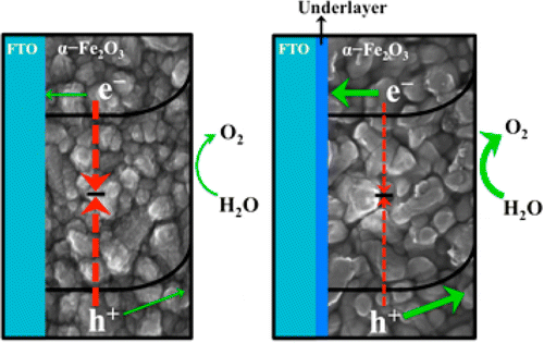
0.6 V versus reversible hydrogen electrode (RHE; slightly positive of the flat band potential). (Picture from graphical abstract).

Growth mechanism and the effect of doping hematite with Ti can be found in this publication: Highly photoactive Ti-doped α-Fe2O3 thin film electrodes: resurrection of the dead layer.


VTT in Finland to spin-off MEMS devices based on novel FABRY-Perot interferometers

According to press release : VTT Technical Research Centre of Finland has developed smart optical measuring devices with companies for uses that include optimisation of vehicle engines, reduction and monitoring of environmental emissions, and quality control of pharmaceuticals. The FABRY research project aimed at utilisation of VTT-developed technologies to enable commercialisation of new products on global markets. So far, two of the companies involved – Rikola Ltd from Finland and InnoPharma Labs from Ireland – have launched products of their own. VTT’s technology makes it possible to miniaturise an entire measuring laboratory to the size of a small sensor.
 
 
Special industry-grade mirror structures realized in the project. (source VTT)
 
Originally, VTT developed these optical measurement technologies and the associated micromechanical Fabry-Perot interferometer components for the purpose of carbon dioxide measurements. The technology has many other applications, however. VTT joined together with eight companies in the Tekes-financed FABRY project in order to create business from the technology in the form of new products.
 
In the course of the project, five of the companies started a product development project of their own based on the project results. So far, two of the companies have launched a new product on the market. Rikola Ltd manufactures and sells the world’s smallest hyperspectral camera, which can be used, for example, for surveying fertilisation and irrigation needs in agricultural areas from UAVs. The Irish InnoPharma Labs manufactures Eyemap cameras for the pharmaceutical industry, facilitating rapid verification of the drug ingredients and their distribution in a tablet.
 
VTT is also in the process of establishing a spin-off company based on this technology, with expected launch in May 2014.
 
“Apart from new business operations, optical measurement technology also has an impact on employment. In the long run, this could create dozens, or maybe even hundreds of new jobs in Finland,” says Jarkko Antila, Senior Scientist at VTT, who has been coordinating the project.
 
 
Tunable MEMS-based Infrared filters. (source VTT)
 
Participants in the 2011–2014 FABRY project (Spectroscopic sensor devices based on novel FABRY-Perot interferometers) coordinated by VTT were Continental Automotive SAS from France (fuel measurements for the automotive industry, onboard sensor); SICK AG from Germany (demanding industrial gas measurements); InnoPharma Labs from Ireland (automatic quality management and control for drug manufacturing in the pharmaceutical industry); Ocean Optics from the United States (optical spectroscopy and Raman spectroscopy); Murata Electronics from Finland (sensor manufacturing for the automotive industry); Rikola Ltd Oy from Finland (cameras for hyperspectral imaging ; manufacturing of spectrometer modules); Okmetic Oyj from Finland (development and manufacturing of high-quality silicon wafer for optical sensor applications) and VTT Memsfab Ltd (manufacturing of MEMS components).
 
Fabry-Perot interferometer
The principle of optical measurement, developed at the end of the 19th century, is a widely used technique, for example in astronomy. Expensive scientific instruments are used to identify and measure different materials based on their characteristic spectral lines, thus obtaining information about the composition of the target. VTT has combined this technology with microelectromechanical systems (MEMS), creating an affordable, very small and adjustable spectral filter. This makes it possible to miniaturise an entire measuring laboratory to the size of a small sensor.
 
Here is a interesting presentation with much more details form Jarkko Antila showing details on ALD MEMS Fabry-Perot interferometer principles and its use for imaging purposes
http://www.vtt.fi/files/newsletter/os/022012/spectral_imaging_device.pdf. It is unclear if this ALD technology is used in the commercial product.

 
Screendump from presentration above

Wednesday, May 14, 2014

How to build your ALD reactors for less than $10,000


A publication on how grad students at Central Michigan University construct ALD reactors for less than $10,000. One hot wall tube reactor and a cold-wall reactor equiped with QCM sensor for in-situ growth studies.

Cost-Effective Systems for Atomic Layer Deposition
Michael Lubitz, Phillip A. Medina, Aleks Antic, Joseph T. Rosin, and Bradley D. 
Publication Date (Web): May 12, 2014
Journal of Chemical Education - (ACS Publications and Division of Chemical Education) http://pubs.acs.org/doi/full/10.1021/ed4007698

Abstract: Herein, we describe the design and testing of two different home-built atomic layer deposition (ALD) systems for the growth of thin films with sub-monolayer control over film thickness. The first reactor is a horizontally aligned hot-walled reactor with a vacuum purging system. The second reactor is a vertically aligned cold-walled reactor with a quartz crystal microbalance (QCM) and a vacuum purging system. This latter reactor was also built to be capable of the addition of liquid- or solution-phase precursors, including the addition of a solution-based precursor containing nanoparticles. Each system cost less than $10,000, and they were used to deposit aluminum oxide thin films using trimethylaluminum and water/isopropyl alcohol as coreactants. Whereas the horizontal hot-walled system was able to deposit alumina thin films at a growth rate of 1.2–1.4 Å/cycle, the more sophisticated vertically aligned reactor deposited films at 0.95–1.1 Å/cycle, which is comparable to commercial systems costing $100,000 or more. Most importantly, both systems were fabricated entirely by M.S. and undergraduate students at Central Michigan University.
 
 
Upper left, a hot-wall tube reactor and right a cold-wall reactor equiped with QCM sensor for in-situ growth studies.(images fromgraphical abstract)  

Monday, May 5, 2014

Denton Vacuum introduces Exilis 1 ALD system

As reported today: Denton Vacuum LLC, a leading manufacturer of thin film technology products, has announced the introduction of Exilis 1, a new atomic layer deposition (ALD) system that will deliver breakthrough results for users in the research, aerospace, optics, semiconductor, and medical communities.
 
DV Model CF-102 ALD Process Chamber (cross-flow thermal). Configured for stand-alone operation or as a Denton Vacuum cluster tool module. Plasma source upgrade will become available in the future (Source Data Sheet).
 
"We've talked to ALD system users all over the world, and they are not happy with what's now available on the market," said Vince McGinty, president and CEO of Denton Vacuum. "Many commercially available ALD systems are limited in capability, while others have proven to be maintenance nightmares, with such simple tasks as chamber cleaning, precursor loading and valve changes turning into complex events that lead to extended, even indeterminate downtime.
"Adding to this," McGinty continued, "users in the corporate community often find that systems designed for research and development bear no resemblance to systems designed for manufacturing-scale activities. Exilis 1 addresses these issues, with broader capability, improved productivity and maintainability, and direct paths to production scale-up."
Denton Vacuum's Exilis 1 brings new capability in several key areas, including:
  • Multi-wafer and 3D component capability.
  • Expanded process chamber adaptability (remote plasma source, a vacuum load lock, and even integration into a Denton cluster tool).
  • An automated load/unload arm that enables immediate, safe removal of hot substrates from the process chamber.
  • Reliable and quick replacement of precursor canisters and ALD valves (the hard-mounted, easy-access manifold incorporates an internal heater assembly, enabling canister or ALD valve changes in less than ten minutes).
For more information regarding Denton's new ALD offering, click here or dwnload the data sheet here.

Sunday, May 4, 2014

Flexible monolayer circuit design by Vanderbilt and ORNL

Vanderbilt University reported - How to create nanowires only three atoms wide with an electron beam - "Junhao Lin, a Vanderbilt University Ph.D. student and visiting scientist at Oak Ridge National Laboratory (ORNL), has found a way to use a finely focused beam of electrons to create some of the smallest wires ever made. The flexible metallic wires are only three atoms wide: One thousandth the width of the microscopic wires used to connect the transistors in today’s integrated circuits."
 
“This will likely stimulate a huge research interest in monolayer circuit design,” Lin said. Because this technique uses electron irradiation, it can in principle be applicable to any kind of electron-based instrument, such as electron-beam lithography.”
 
One of the intriguing properties of monolayer circuitry is its toughness and flexibility. It is too early to predict what kinds of applications it will produce, but “If you let your imagination go, you can envision tablets and television displays that are as thin as a sheet of paper that you can roll up and stuff in your pocket or purse,” Pantelides commented.
 
In addition, Lin envisions that the new technique could make it possible to create three-dimensional circuits by stacking monolayers “like Lego blocks” and using electron beams to fabricate the wires that connect the stacked layers.
 
Full report from Vanderbilt University can be found here and please check out the video and the publication below for more insights!


Series of still scanning electron micrographs (a to d) show how the electron beam is used to create nanowires. (Junhao Lin / Vanderbilt)


Junhao Lin, a Vanderbilt University Ph.D. student and visiting scientist at Oak Ridge National Laboratory (ORNL), has found a way to use a finely focused beam of electrons to create flexible metallic wires that are only three atoms wide: One thousandth the width of the microscopic wires used to connect the transistors in today's integrated circuits and some of the smallest wires ever made. The discovery gives a boost to efforts aimed at creating electrical circuits on monolayered materials, raising the possibility of flexible, paper-thin tablets and television displays. [youtube.com]

Atomic mechanism of the semiconducting-to-metallic phase transition in single-layered MoS2
Yung-Chang Lin, Dumitru O. Dumcenco, Ying-Sheng Huang & Kazu Suenaga        
Nature Nanotechnology (2014) doi:10.1038/nnano.2014.64 Published online 20 April 2014
 
Abstract:
Phase transitions can be used to alter the properties of a material without adding any additional atoms and are therefore of significant technological value. In a solid, phase transitions involve collective atomic displacements, but such atomic processes have so far only been investigated using macroscopic approaches. Here, we show that in situ scanning transmission electron microscopy can be used to follow the structural transformation between semiconducting (2H) and metallic (1T) phases in single-layered MoS2, with atomic resolution. The 2H/1T phase transition involves gliding atomic planes of sulphur and/or molybdenum and requires an intermediate phase (α-phase) as a precursor. The migration of two kinds of boundaries (β- and γ-boundaries) is also found to be responsible for the growth of the second phase. Furthermore, we show that areas of the 1T phase can be controllably grown in a layer of the 2H phase using an electron beam.
 

Saturday, May 3, 2014

3rd China ALD conference Shanghai, October 16 to 17, 2014

The 2nd International Conference on ALD Applications / 3rd China ALD conference will be a two-day meeting, dedicated to the fundamental, materials, and applications of Atomic Layer Deposition (ALD) technology. It will be held in Shanghai, China, from October 16 to 17, 2014. Following the success of the 1st and 2nd China ALD Scientific Meeting in 2010 and 2012, the 3rd China ALD 2014 conference will feature plenary sessions, poster sessions and an industrial exhibition.


Organization Commmittee:

ORGANIZING CHAIRS : Prof. Shi-Jin Ding and Prof. Yongfeng Mei
     
SECRETARY-GENERAL : Asso. Prof. Hongliang Lu and Asso. Prof. Feng Zhang


Invited Speakers (Confirmed)


Prof. Steve George, University of Colorado at Boulder
Title: Spatial Atomic Layer Deposition on Flexible Substrates Using a Modular Rotating Cylinder

Prof. Gregory Parsons, North Carolina University
Title: New Applications and Ab-Initio Reaction Mechanism Analysis for ALD onto Polymer Fibers and Films Abstract

Prof. Erwin Kessels, Technische Universiteit Eindhoven
Title: Surface chemistry during metal ALD: Opportunities for film growth, nanopatterning and nanoparticle synthesis

Prof. Christophe Detavernier, Ghent University
Title: Thermal and Plasma Enhanced Atomic Layer Deposition on Powders Abstract

Prof. Hyeongtag Jeon, Hanyang University
Title: Multi-density ALD Al2O3 Layer for OLED Abstract

Prof. Yukihiro SHIMOGAKI, University of Tokyo

Prof. Peide Ye, Purdue University
Title: ALD for State-Of-The-Art Nanoelectronics Abstract

Prof. Stacey F. Bent, Stanford University
Title: ALD of Nanoscale Materials for Energy Conversion Applications Abstract

Prof. Mato Knez, Nanoscience Cooperative Research Center

Prof. Jane P. Chang, University of California at Los Angeles
Title: Enabling the Synthesis and Integration of Multiferroic Materials by Atomic Layer Processing

Prof. Hyungjun Kim, Yonsei University
Title: Synthesis of 2D Transition Metal Disulfides (TMDSs) Nanosheets using Atomic Layer Deposition Abstract

Prof. Yong Wang, Nanjing Tech University
Title: Atomic layer deposition for the modification and functionalization of separating membranes: chances and challenges Abstract

Prof. Markku Leskela, University of Helsinki
Title: ALD for Energy Applications Abstract

Program is now available here.

Tuesday, April 29, 2014

Picosun Oy, demonstrates functional ALD coatings for novel, ecological catalyst materials

As reported by Picosun today : Picosun Oy, the leading manufacturer of high quality Atomic Layer Deposition (ALD) equipment, extends its solution portfolio into functional ALD coatings for novel, ecological catalyst materials.
 
The now developed novel catalysts are aimed to significantly reduce costs and process waste generation of chemical manufacturing. Potentially, this can lead to several hundreds of millions of euros economic impact, giving a substantial boost to the competitive edge and sustainability of European chemical and pharmaceutical industries.
 
Picosun's ALD technology enables optimized deposition of catalytically active metals on simple, cost-efficient supports such as metal oxide or polymer powders, thus realizing highly efficient catalytic function with only a fraction of cost compared to traditional catalyst technologies. As a tightly contained and controlled gas-phase process, ALD also eliminates the risks of typical wet chemistry methods such as leaks, environmental contamination, and material waste.


"The now developed catalyst technology on powder substrates is an invaluable addition to our extensive ALD solution portfolio. There is a significant market for Picosun's ALD expertise in the field of chemical and pharmaceuticals manufacturing. In addition to these industries, our optimized powder coating methods can outperform current solutions for example in the automotive industries and in the next generation lithium ion thin film battery manufacturing," summarizes Juhana Kostamo, Managing Director of Picosun.


The development work for ALD-enabled catalyst manufacturing was realized within the frame of European Union 7th Framework project POLYCAT ("Modern polymer-based catalysts and microflow conditions as key elements of innovations in fine chemical synthesis"), running from October 2010 to April 2014.


Monday, April 28, 2014

Video from Lam Research - how innovative technology has changed our lives

Nice promotion video from Lam Research - See how innovative technology has changed our lives. See how Lam's capital equipment and services have enabled the breathtaking rate of advancement in the semiconductor industry.

 
Screendump


Sunday, April 27, 2014

40 years since Tuomo Suntola designed and demonstrated a humidity sensor at VTT for Vaisala

As reported by Vaisala : "In the early 1970s, humidity was measured using organic materials, such as human or animal hair, in hygrometers. At the time there were few alternatives available and the accuracy and reliability issues of such measurement methods were well known. In an effort to find a solution, Vaisala contracted the semiconductor laboratory of the Technical Research Center of Finland to cooperate on the development of sensors. As a result of this work, Vaisala introduced HUMICAP®, the world’s first thin-film capacitive humidity sensor in 1973." [Idea for this blog post from Riikka Puurunen, via LinkedIn - thank you very much]
 

Dr. Suntola [ALD Inventer] first industrial work was “Humicap®” thin film humidity sensor for Vaisala Oy (1973) which still, almost 40 years later holds the world market leader’s position in humidity sensing (http://www.sci.fi/~suntola/biography.html) [screen dump from video below]
Below you can  watch a video clip about the birth of HUMICAP®. More information on the Vaisala HUMICAP® for downloead here.


This celebration was really last year (2013). More information and other stories from Finland will be presented at the exhibition "40 Years of ALD in Finland". General celebration the Baltic ALD conference 2014, May 12-13, Helsinki, Finland (Twitter tag #FinALD40).

"The conference is a continuation of a series of meetings that started in 1991 in Espoo as a Helsinki University of Technology – Tartu University ALE symposium, followed by a symposium in Tartu in 1993. In 1995 the meeting was organized by University of Helsinki and at that time the name was broadened to Baltic ALE symposium. In 1997 in Tartu it adopted its present name and has subsequently circled around the Baltic Sea in Uppsala, Oslo, Warsaw and Hamburg besides Finland and Estonia.
 
The present conference also celebrates 40 years of ALD technology as it was in 1974 when Dr. Tuomo Suntola and collaborators began their seminal work that made ALD a valuable industrial technology, first for electroluminescent display production and later for microelectronics and ever increasing other application areas."

Toshiba Corporation starting 15nm 128-gigabit NAND flash at Fab 5 Yokkaichi

Toshiba Corporation announced that it has developed the world's first 15-nanometer (nm) process technology, which will apply to 2-bit-per-cell 128-gigabit (16 gigabytes) NAND flash memories. Mass production with the new technology will start at the end of April at Fab 5 Yokkaichi Operations, Toshiba's NAND flash fabrication facility (fab), replacing second generation 19 nm process technology, Toshiba's previous flagship process. The second stage of Fab 5 is currently under construction, and the new technology will also be deployed there.

Read more at Tweaktown.
 
 
"In-keeping with semiconductor industry fast-track construction techniques and schedules, Toshiba and manufacturing partner, SanDisk have officially opened their third 300mm wafer NAND flash fabrication facility at Toshiba's Yokkaichi Operations in Mie Prefecture, Japan, dubbed Fab 5." (Fabtech)

If you want to take a visit Google Street View offers excellent view from the Toshiba site in Yokkaichi. Just tune in here in this intersection take a right turn and enjoy the drive : Toshiba Fab 5.

 
Screendump from Google Street View just upfront of Toshiba Fab 5 in Yokkaichi.


Saturday, April 26, 2014

By V-NAND Samsung is set for more advanced products including terabit NAND flash memory

Recently this picture below was published on LinkeIn (I seen it posted by Yangyin Chen
陈杨胤, researcher at imec) and other social media and has been shared a great deal. Naturally there has been comments and questions if it will go on on heading for 128 terabit NAND flash memory 2025 or so.
 
 
To get a glimpse into how this scaling has been possible I checked out the Samsung information on V-NAND as they call their 3D-NAND technology. According to the information available on Samsungs web they have set the foundation for more advanced products including 512 gigabit (Gb) and one terabit (Tb) NAND flash memory, which we expect to develop within the next few years. structure. So single digit terabit should not be a problem. What about 128 TB? I don´t know, but I assume we will need that integrated into a Google lens to record our exiting lives in 3D-HD feeding real time in to Facebook accounts pretty soon :-)  
 
 
Samsung’s new V-NAND offers a 128 gigabit (Gb) density in a single chip, utilizing the company’s proprietary vertical cell structure based on 3D Charge Trap Flash (CTF) technology and vertical interconnect process technology to link the 3D cell array. By applying both of these technologies, Samsung’s 3D V-NAND is able to provide over twice the scaling of 20nm-class planar NAND flash.By making this CTF layer three-dimensional, the reliability and speed of the NAND memory have improved sharply. The new 3D V-NAND shows not only an increase of a minimum of 2X to a maximum 10X higher reliability, but also twice the write performance over conventional 10nm-class floating gate NAND flash memory. [Far East Gizmos]

Picture showing 3D stacking up to 24 layers (from Iter news http://itersnews.com/?p=68244)
 
   "An industry first, it represents a breakthrough in overcoming the density limit currently facing the planar NAND architecture and floating gates used in conventional flash memory, as well as yielding speed and endurance" 

Check out the promo video from Samsungs YouTube channel below.


BENEQ installed new ALD equipment at University of Bath

A new Atomic Layer Deposition (ALD) Suite, installed in the Department of Chemistry this week, will allow researchers to deposit thin films of molecules onto surfaces with greater precision than ever before.
 
 
DTC students Joe Thompson and Andrew Rushworth watch as Dr Jeff Hamilton makes some final adjustments (picture from University of Bath press release)
 

Technicians and staff from Beneq, who manufactured the equipment, have been working with Dr Andrew Johnson and Professor Michael Hill to deliver the new facility. They have trained three DTC PhD students alongside post-doctoral researcher Dr Jeff Hamilton in a series of new ALD techniques using the equipment.
 
ALD involves depositing ultra-thin layers of material, using either plasma or thermal deposition methods. The device is also integrated with a Quadrupole mass analyzer, which will enable close monitoring of deposition products and processes.
This exciting new piece of equipment will play an important role in many Doctoral Training Centre (DTC) research projects projects. Ibbi Ahmet, a second-year PhD student in the DTC supervised by Dr Johnson and co-supervised by Professor Hill and Professor Simon Bending (Department of Physics), said:
''Exciting times are ahead of us and we hope to trial many of the novel ALD precursors we have been developing over the past few years in order to produce materials, such as graphene, molybdenum disulfide, tin disulfide and tungsten disufide layers.''

ALD - Standard Operating Procedures for a Cambridge Nanotech reactor


As reported on Youtube by INRF - The Integrated Nanosystems Research Facility at the University of California, Irvine (INRF UCI) - here are some really good and detailed insights into how to grow Al2O3 and HfO2 by ALD using a Savannah Cambridge Nantech reactor. Their Youtube channel have additional instruction movise from their clean room that you might find interesting. Who doesn´t clean room movies!?!? :-)


Usage Policies for Cambridge Nanotech ALD System and standard policies for usage. This document provides the standard operation procedure of the Cambridge Nanotech ALD. System in the INRF cleanroom at UCI. The ALD system allows to deposit Al2O3 and HfO2 thin films atomic layer by layer onto silicon based substrate.
 
This tool is equipped with high-speed pneumatic pulse valves to enable our unique Exposure Mode™ for thin film deposition on Ultra High Aspect Ratio substrates. This proven precision thin film coating methodology can be used to deposit conformal, uniform films on substrates with aspect ratios of greater than 2000:1. This system is equipped with heated precursors lines and the option to add up to six precursor lines.
 
View the SOP documentation or check out the great instruction movie below.
http://www.inrf.uci.edu/sop-ald/


Friday, April 25, 2014

IBM and National Geographic Kids Unveil GUINNESS WORLD RECORD Title

National Geographic Kids today claimed its ninth GUINNESS WORLD RECORDS® title for the Smallest Magazine Cover, using technology from IBM, at the USA Science & Engineering Festival in Washington, D.C. To create the record-setting cover, IBM scientists invented a tiny "chisel" with a heatable silicon tip 100,000 times


Full story can be found in this press release and check out the video below.


Paper-based ultracapacitors with carbon nanotubes-graphene composites

As reported by EE Times: Ultracapacitors, also called supercapacitors, serve as temporary energy storage that can quickly charge and discharge for everything from regenerative brakes in electric vehicles to cordless power tools that recharge in 90 seconds to stabilizing computer power supplies. Now researchers at George Washington University's Micro-Propulsion and Nanotechnology Laboratory report that superior ultracapacitors can be constructed from an inexpensive hybrid composite of graphene flakes mixed with single-walled carbon nanotubes.
 
Full report can be found in the JAP paper below


Prototype of an ultracapacitor device based on carbon nanostructures.

Paper-based ultracapacitors with carbon nanotubes-graphene composites
Jian Li, Xiaoqian Cheng, Jianwei Sun, Cameron Brand, Alexey Shashurin, Mark Reeves and
Michael Keidar
J. Appl. Phys. 115, 164301 (2014); http://dx.doi.org/10.1063/1.4871290

In this paper, a paper-based ultracapacitors were fabricated by the rod-rolling method with the ink of carbon nanomaterials, which were synthesized by arc discharge under various magnetic conditions. Composites of carbon nanostructures, including high-purity single-walled carbon nanotubes (SWCNTs) and graphene flakes were synthesized simultaneously in a magnetically enhanced arc. These two nanostructures have promising electrical properties and synergistic effects in the application of ultracapacitors. Scanning electron microscope, transmission electron microscope, and Raman spectroscopy were employed to characterize the properties of carbon nanostructures and their thin films. The sheet resistance of the SWCNT and composite thin films was also evaluated by four-point probe from room temperature to the cryogenic temperature as low as 90 K. In addition, measurements of cyclic voltammetery and galvanostatic charging/discharging showed the ultracapacitor based on composites possessed a superior specific capacitance of up to 100 F/g, which is around three times higher than the ultracapacitor entirely fabricated with SWCNT.

Tuesday, April 22, 2014

Spatial atmospheric ALD - a new laboratory and industrial tool for low-cost photovoltaics

A Mini Review on atmospheric Spatial ALD for PV applications. Spatial atmospheric atomic layer deposition: a new laboratory and industrial tool for low-cost photovoltaics:

Spatial atmospheric atomic layer deposition: a new laboratory and industrial tool for low-cost photovoltaics

David Muñoz-Rojas and Judith MacManus-Driscoll 

Mater. Horiz., 2014,1, 314-320 DOI: 10.1039/C3MH00136A
Abstract

Recently, a new approach to atomic layer deposition (ALD) has been developed that doesn't require vacuum and is much faster than conventional ALD. This is achieved by separating the precursors in space rather than in time. This approach is most commonly called Spatial ALD (SALD). In our lab we have been using/developing a novel atmospheric SALD system to fabricate active components for new generation solar cells, showing the potential of this novel technique for the fabrication of high quality materials that can be integrated into devices. In this minireview we will introduce the basics of SALD and illustrate its great potential by highlighting recent results in the field of photovoltaics.
 
 
Image from graphical abstract (Materials Horizons)


Trinity College Dublin showcase production of graphene by shear mixing

To progress from the laboratory to commercial applications, it will be necessary to develop industrially scalable methods to produce large quantities of defect-free graphene. Trinity College Dublin Ireland show that high-shear mixing of graphite in suitable stabilizing liquids results in large-scale exfoliation to give dispersions of graphene nanosheets.

Or as The Daily Mail puts it "How to make a supermaterial in the sink: Scientists find washing up liquid and a blender can be used to make graphene"
Scalable production of large quantities of defect-free few-layer graphene by shear exfoliation in liquids

Keith R. Paton, Eswaraiah Varrla, Claudia Backes, Ronan J. Smith, Umar Khan, Arlene O’Neill, Conor Boland, Mustafa Lotya, Oana M. Istrate, Paul King, Tom Higgins, Sebastian Barwich, Peter May, Pawel Puczkarski, Iftikhar Ahmed, Matthias Moebius, Henrik Pettersson, Edmund Long, João Coelho, Sean E. O’Brien, Eva K. McGuire, Beatriz Mendoza Sanchez, Georg S. Duesberg, Niall McEvoy, Timothy J. Pennycook, Clive Downing, Alison Crossley, Valeria Nicolosi & Jonathan N. Coleman
 
Nature Materials DOI: doi:10.1038/nmat3944 Published online:
 
To progress from the laboratory to commercial applications, it will be necessary to develop industrially scalable methods to produce large quantities of defect-free graphene. Here we show that high-shear mixing of graphite in suitable stabilizing liquids results in large-scale exfoliation to give dispersions of graphene nanosheets. X-ray photoelectron spectroscopy and Raman spectroscopy show the exfoliated flakes to be unoxidized and free of basal-plane defects. We have developed a simple model that shows exfoliation to occur once the local shear rate exceeds 104 s−1. By fully characterizing the scaling behaviour of the graphene production rate, we show that exfoliation can be achieved in liquid volumes from hundreds of millilitres up to hundreds of litres and beyond. The graphene produced by this method performs well in applications from composites to conductive coatings. This method can be applied to exfoliate BN, MoS2 and a range of other layered crystals.
 
 
Production of graphene by shear mixing (graphical abstract Nature Materials)
 

Monday, April 21, 2014

LG and researchers at ETH Zürich announce graphene membrane breakthrough

As reported by Solid State Technology : "Researchers from LG Electronics (LG) and Swiss university ETH Zurich (Swiss Federal Institute of Technology Zurich) have developed a method to greatly increase the speed and efficient transmission of gas, liquid and water vapor through perforated graphene, a material that has seen an explosion of scientific interest in recent years. The findings open up the possibility in the future to develop highly efficient filters to treat air and water. [...]  developed a reliable method for creating 2D membranes using chemical vapor deposition (CVD) optimized to grow graphene with minimal defects and cracks to form graphene layers thinner than 1nm (nanometer). Using a focused ion beam (FIB), the researchers then drilled nanopores in double layers of graphene to produce porous membranes with aperture diameters between less than 10nm and 1µm (micrometer). Testing various sized perforations, the researchers found that their graphene membrane resulted in water permeance five- to sevenfold faster than conventional filtration membranes and transmission of water vapor several hundred times higher compared to today’s most advanced breathable textiles such as Gore-Tex."
 
 
The full report by Kemal Celebi et al can be read in Science publication below:
 

Kemal Celebi, Jakob Buchheim, Roman M. Wyss, Amirhossein Droudian, Patrick Gasser, Ivan Shorubalko, Jeong-Il Kye, Changho Lee, Hyung Gyu Park

Science 18 April 2014: Vol. 344 no. 6181 pp. 289-292,  DOI: 10.1126/science.1249097                        
A two-dimensional (2D) porous layer can make an ideal membrane for separation of chemical mixtures because its infinitesimal thickness promises ultimate permeation. Graphene—with great mechanical strength, chemical stability, and inherent impermeability—offers a unique 2D system with which to realize this membrane and study the mass transport, if perforated precisely. We report highly efficient mass transfer across physically perforated double-layer graphene, having up to a few million pores with narrowly distributed diameters between less than 10 nanometers and 1 micrometer. The measured transport rates are in agreement with predictions of 2D transport theories. Attributed to its atomic thicknesses, these porous graphene membranes show permeances of gas, liquid, and water vapor far in excess of those shown by finite-thickness membranes, highlighting the ultimate permeation these 2D membranes can provide.

Saturday, April 19, 2014

Video : Understanding the new FinFET semiconductor transistor technology


The FinFET process is a way to stack additional transistors onto the silicon, thereby making faster and more power-efficient chip. For an explainer on the manufacturing process, watch the video below. The term FinFET was coined by University of California, Berkeley researchers (Profs. Chenming Hu, Tsu-Jae King-Liu and Jeffrey Bokor) to describe a nonplanar, double-gate transistor built on an SOI substrate. The distinguishing characteristic of the FinFET is that the conducting channel is wrapped by a thin silicon "fin", which forms the body of the device. The Wrap-around gate structure provides a better electrical control over the channel and thus helps in reducing the leakage current and overcoming other short channel effects. In current usage the term FinFET has a less precise definition. Among microprocessor manufacturers, AMD, IBM, and Freescale describe their double-gate development efforts as FinFET development whereas Intel avoids using the term to describe their closely related tri-gate architecture. In the technical literature, FinFET is used somewhat generically to describe any fin-based, multigate transistor architecture regardless of number of gates. In 2012, Intel started using FinFETs for its future commercial devices. In September 2012, Globalfoundries announced plans to offer a 14-nanometer process technology featuring FinFET three-dimensional transistors in 2014. The next month, the rival company TSMC, announced start early or "risk" production of 16 nm FinFETS in November 2013.[adopted from Wikipedia]
 
Recently Samsung and Globalfoundries announced an agreement between the two companies would see Samsung develop a 14nm process node and license it to Globalfoundries.


Screendump showing the ALD high-k dielectric and TiN metal gate wrapping the fin conformally.


This Globalfoundries factory near Albany, New York, will adopt a production process developed by Samsung. Kelvin Low, senior director of marketing for Samsung's North American foundry operations, said its 14-nanometer process is already being used to produce some customer chips in small quantities. It predicts volume production by the end of 2014 using the process, which will be introduced at two factories in South Korea as well as Austin. [Source WSJ]


Friday, April 18, 2014

Han-Yang University held ‘10th Korean ALD Workshop’ at Baek-Nam Academy Information Center

Han-Yang University held ‘10th Korean ALD Workshop’ at Baek-Nam Acedemy Information Center 6th Fl. International Conference Room, Seong-Dong Gu, Seoul. ALD is one of the technologies we the Koreans are leading in the semiconductor material fields and the technology of our ALD tools and material technologies are recognized worldwide.

"I have hosted this important workshop last 10 years. This year the attendees were over 300 and Hall was very crowded and there were 8 invited speakers and Steve and Greg were among them." said Professor Jeon at Han-Yang University.


Participants:
Greg Parsons, Professor of North Carolina State University
Steven George, Professor of Colorado University
Ki-Bum Kim, Professor of Material Engineering, Seoul National University
Si-Woo Lee, Professor of Chemical Engineering, Postech
And the other internationally known experts.


Invited speakers to the 10th Korean ALD Workshop including: Greg Parsons, Professor of North Carolina State University, Steven George, Professor of Colorado University, Ki-Bum Kim, Professor of Material Engineering, Seoul National University, Si-Woo Lee, Professor of Chemical Engineering, Postech (Picture from organizer Prof. Jeon Professor Jeon at Han-Yang University).

Growth and stacking 2D materials MoS2, WSe2, and hBN on epitaxial graphene by CVD

Researchers at Penn State's Center for 2-Dimensional and Layered Materials and the University of Texas at Dallas have shown the ability to grow high quality, single-layer materials one on top of the other using CVD (chemical vapor deposition). Furthermore, they have demonstrated growth and stacking 2D materials MoS2, WSe2, and hBN on epitaxial graphene by CVD.  

 
The stacking of two-dimensional layered materials: MoS2, WSe2, and hBN on epitaxial graphene (Picture from graphical abstract:ACS Nano, DOI: 10.1021/nn5003858)
 
 
Read more at Nanowerk: Making new materials an atomic layer at a time or in the publication below.
Direct Synthesis of van der Waals Solids

Yu-Chuan Lin, Ning Lu, Nestor Perea-Lopez, Jie Li, Zhong Lin, Xin Peng, Chia Hui Lee, Ce Sun, Lazaro Calderin, Paul N. Browning, Michael S. Bresnehan, Moon J. Kim, Theresa S. Mayer, Mauricio Terrones , and Joshua A. Robinson

ACS Nano, Article ASAP, DOI: 10.1021/nn5003858, Publication Date (Web): March 18, 2014

Abstract:
The stacking of two-dimensional layered materials, such as semiconducting transition metal dichalcogenides (TMDs), insulating hexagonal boron nitride (hBN), and semimetallic graphene, has been theorized to produce tunable electronic and optoelectronic properties. Here we demonstrate the direct growth of MoS2, WSe2, and hBN on epitaxial graphene to form large-area van der Waals heterostructures. We reveal that the properties of the underlying graphene dictate properties of the heterostructures, where strain, wrinkling, and defects on the surface of graphene act as nucleation centers for lateral growth of the overlayer. Additionally, we show that the direct synthesis of TMDs on epitaxial graphene exhibits atomically sharp interfaces. Finally, we demonstrate that direct growth of MoS2 on epitaxial graphene can lead to a 103 improvement in photoresponse compared to MoS2 alone.


A photosensor fabricated on the MoS2/graphene heterostructure. (Image: Yu-Chuan Lin, Penn State)

Tuesday, April 15, 2014

More Three-Dimensional Nanofabrication using Block Copolymer Self-Assembly by KAIST

In a recent blog post here reported about KAIST and others presented "ALD Assisted Pattern Multiplication of Block Copolymer for 5 nm Scale Nanopatterning". There seems to be no end to this topic here is a more full coverage in the form of a review paper "Three-Dimensional Nanofabrication using Block Copolymer Self-Assembly" [Free to download - thank you very much indeed!] work by KAIST.

“Three-Dimensional Nanofabrication by Block Copolymer Self-Assembly”

Caroline A. Ross*, Karl K. Berggren, Joy Y. Cheng, Yeon Sik Jung,* and Jae-Byum
Advanced Materials, 2014, published online

Thin films of block copolymers are widely seen as enablers for nanoscale fabrication of semiconductor devices, membranes, and other structures, taking advantage of microphase separation to produce well-organized nanostructures with periods of a few nm and above. However, the inherently threedimensional structure of block copolymer microdomains could enable them to make 3D devices and structures directly, which could lead to effi cient fabrication of complex heterogeneous structures. This article reviews recent progress in developing 3D nanofabrication processes based on block copolymers.

 
Check out this great page with access to most of the papers from The Functional Nanofabrication Lab at KAIST as free download - FUNNANO!
 

Beneq is joining forces with German MBRAUN for OLED

In a press release on April 15, 2014, Beneq announced that it is joining forces with MBRAUN to address the growing OLED market needs by offering turn-key R&D solutions. The goal is to enforce rapid adaptation of Beneq’s breakthrough thin-film encapsulation technology in OLED research and manufacturing.

Beneq and MBRAUN currently have a mutually supportive offering, which will allow customers to get a wider portfolio of products and services from a single source. These products are primarily targeted to those customers with sophisticated needs in OLED research, especially in the area of thin-film encapsulation. For each customer need, Beneq and MBRAUN will work together to tailor products and services that best meet the specific clean environment requirements in question.
 
 
Beneq and MBRAUN are joining forces to boost thin film encapsulation for OLED research and manufac-turing. Picture: Beneq.
 
More details can be found here in this slide share file.