Tokyo Electron (TEL) achieved a record-breaking financial year in FY2025, with strong top- and bottom-line growth driven by robust global demand for advanced semiconductor equipment. Net sales rose by 32.8% year-on-year to approximately ¥2.43 trillion (around $15.7 billion USD), marking the highest in the company's history. Operating profit surged to ¥697.3 billion (about $4.5 billion USD), supported by an improved operating margin of 28.7%. Growth was underpinned by increased investment in leading-edge logic and memory, particularly High Bandwidth Memory (HBM) and advanced DRAM nodes, where TEL maintained or expanded market share through key Process of Record (POR) wins in etch and wafer bonding technologies. Revenue contributions diversified geographically, with notable gains in South Korea and Taiwan, even as China remained a key market. TEL also demonstrated strong cash flow, increased its R&D and capital investments, and returned significant value to shareholders through dividends and buybacks. Looking ahead, TEL forecasts continued growth in FY2026, positioning itself to capitalise on accelerating AI, 2nm logic, and heterogeneous integration trends.
Tokyo Electron TEL has demonstrated strong financial performance and strategic market expansion through FY2025, according to their investor presentation dated April 30, 2025. Their net sales, gross profit, operating profit, and net income have all reached record highs, signaling both operational efficiency and favorable market conditions.
LINK: Tokyo Electron Limited 2025 Q4 - Results - Earnings Call Presentation (OTCMKTS:TOELY) | Seeking Alpha
Tokyo Electron's Q4 FY2025 earnings call highlighted strong financial performance and an optimistic forward outlook amid geopolitical uncertainties. Despite global concerns around US tariffs and export controls—particularly in China, which saw its WFE market share fall to 35%—TEL stated that it has not observed any significant changes in customer investment sentiment or competitive dynamics. The company reaffirmed its strategy of focusing on long-term innovation rather than short-term regulatory shifts, underscoring its commitment to developing higher-productivity tools to offset potential external headwinds. Looking ahead, TEL forecasts continued double-digit WFE market growth into calendar 2026, driven by AI infrastructure demand, 2nm logic, and HBM scaling. The company plans record-high investments of ¥300 billion in R&D and ¥240 billion in CapEx for FY2026, reflecting confidence in sustained momentum across DRAM, advanced logic, and packaging technologies. TEL aims to expand global market share and reach ambitious mid-term goals, including over ¥1 trillion in operating profit and 35%+ OPM, by capitalising on technology transitions such as GAA, backside PDN, and heterogeneous integration.
LINK: Tokyo Electron Limited (TOELY) Q4 2025 Earnings Call Transcript | Seeking Alpha
Revenue and Profitability Growth:
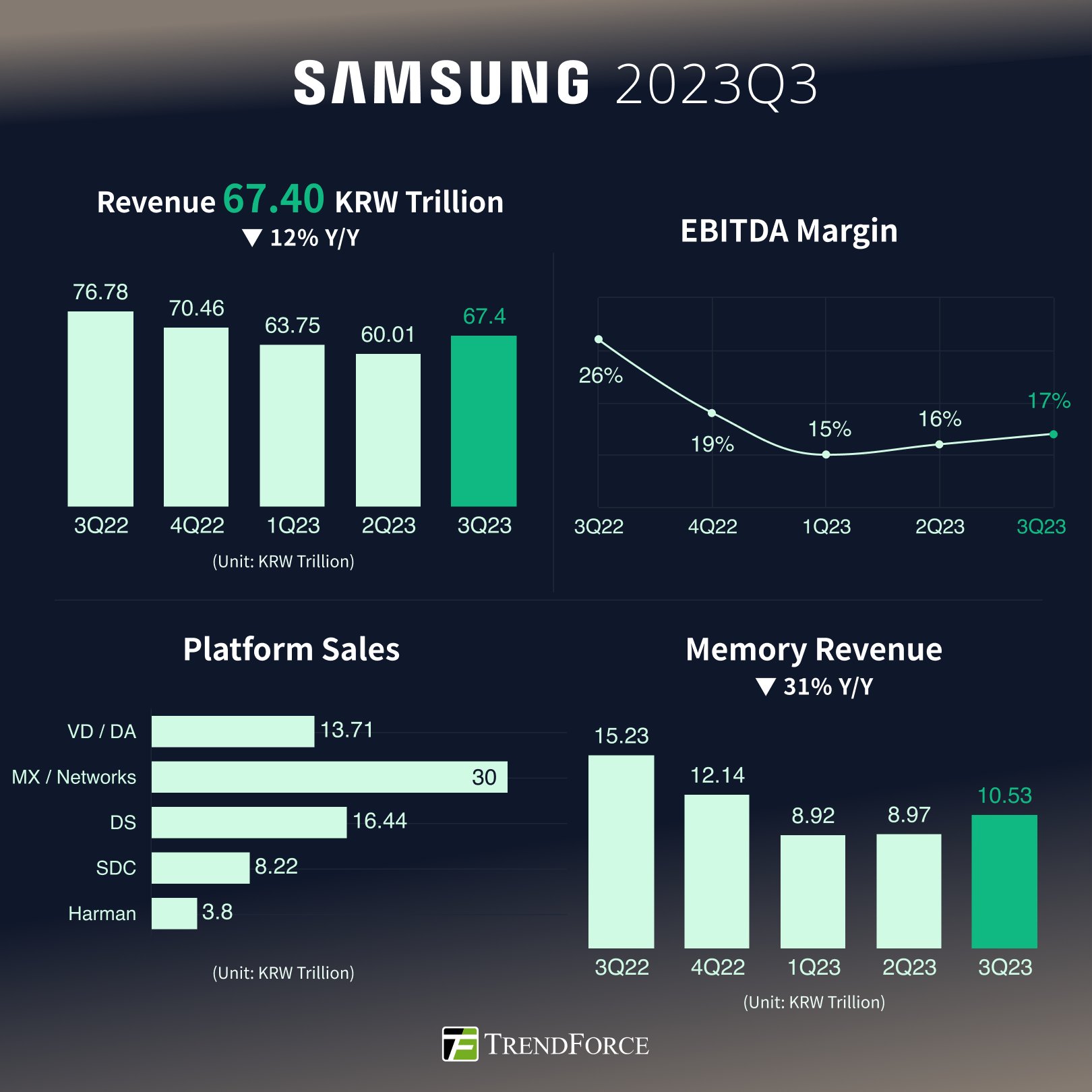
Net sales increased significantly from ¥1,399.1 billion in FY2021 to ¥2,431.5 billion in FY2025, a 74% increase over four years. The gross profit also rose steadily, reaching ¥1,146.2 billion in FY2025, up from ¥564.9 billion in FY2021. Operating profit followed suit, more than doubling from ¥320.6 billion to ¥697.3 billion. These trends underscore TEL’s ability to scale profitably, with operating margins rising from 22.9% in FY2021 to 28.7% in FY2025. Return on equity (ROE) also remained strong, peaking at 37.2% in FY2022 and settling at 30.3% in FY2025, a testament to effective capital management.
Regional Sales Composition:
The revenue breakdown by region from Q1 FY2024 to Q4 FY2025 shows growing diversification. Notably, China has remained the single largest market, although its share declined from 47.4% in Q4 FY2024 to 34.3% in Q4 FY2025, reflecting a strategic balancing across geographies. South Korea, Taiwan, and North America significantly increased their contributions, with South Korea reaching ¥147.0 billion and Taiwan ¥135.8 billion in Q4 FY2025. This reflects growing demand from advanced logic and memory fabrication customers in these regions.

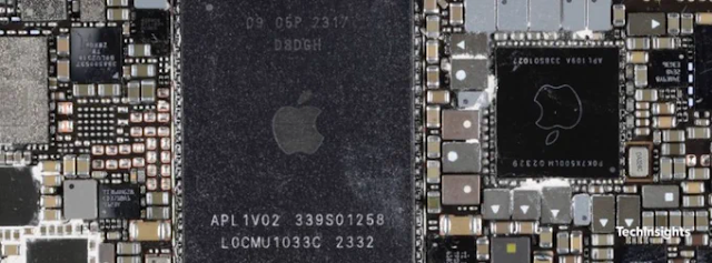
In FY2025, Tokyo Electron’s semiconductor production equipment (SPE) sales reached ¥1.86 trillion, driven by a sharp rise in DRAM-related investments, particularly for high-bandwidth memory (HBM), which accounted for 31% of total sales. Non-volatile memory (NAND) remained stable at 7%, while non-memory segments, including logic and foundry, continued to dominate with 62%, reflecting robust demand from both advanced and mature nodes. The overall recovery and expansion of customer investments across segments underpinned this strong performance.
Market Segment Performance
Tokyo Electron’s global market share in CY2024 demonstrates its leadership across multiple core segments of the semiconductor production equipment market. The company holds a commanding 92% share in coater/developer systems, underlining its unparalleled position in photoresist processing for advanced lithography applications. It also leads the wafer prober segment with a 38% share and maintains robust positions in key deposition categories, including 38% in CVD and 37% in oxidation/diffusion systems. In contrast, TEL’s market share in ALD stands at 16%, notably behind ASM International, highlighting an opportunity for expansion in this strategically important technology as the industry moves towards GAA and other 3D device structures. Performance in dry etch (27%), cleaning systems (21%), and wafer bonding (32%) rounds out a broadly competitive portfolio that positions TEL to effectively support ongoing advancements in scaling, heterogeneous integration, and high-performance packaging across logic, memory, and AI-related applications.

To further expand our future profit, we made steady progress in penetrating into new technology domains. Specifically, we released multiple new outstanding products contributing to the semiconductor technology innovation. For example, penetration to untapped segments such as single-wafer plasma CVD and PVD, gas cluster beam system which improves efficiency of leading-edge lithography, and laser-lift-off system to drastically decrease environmental footprint of processing. In fiscal 2025, we conducted share repurchase of about ¥150 billion in total.
- Toshiki Kawai - Representative Director, President and CEO
New product 2025 Episode™ single-wafer CVD platform
Episode™ 1 is Tokyo Electron's latest single-wafer CVD platform, launched in 2024 to address the challenges of advanced device scaling in logic, DRAM, and future AI processors. It supports up to eight process modules, enabling complex, uninterrupted multi-step processing. The system integrates the OPTCURE™ module for native oxide removal and ORTAS™ for titanium CVD, allowing immediate Ti deposition to minimise contact resistance in advanced interconnects. Episode™ 1 replaces traditional PVD with CVD to achieve uniform, low-resistivity films in high aspect ratio structures such as deep contact holes. With a 45% smaller footprint than its predecessor and advanced edge computing, data analytics, and environmental tracking capabilities, the system enhances fab productivity, engineer efficiency, and readiness for new materials in next-generation device manufacturing.
The TEL Episode™ 1 system shown in the image seems to feature twin or dual single-wafer process chambers, which is typical in modular CVD tools designed for high throughput. Each visible module (with two load ports per unit) likely contains two process chambers within the same footprint to maximise wafer handling efficiency and enable parallel processing—common in tools aimed at advanced logic and memory manufacturing.
Episode™ 1 offers a reduced footprint. Compared with the Triase+™ series, twice as many smaller modules can be installed in a system. With the same number of modules installed, Episode™ 1 takes up about 45% less fab space than its predecessor
LINK: Episode™ 1 Single-Wafer Deposition System for Semiconductors: Driving the Evolution of AI Semiconductors to Transform Everyday Life | Blog | Tokyo Electron Ltd.


%20(1).png)