Showing posts with label memory. Show all posts

Wednesday, November 1, 2023

Surge in HBM Demand Marks Memory Market Recovery and Anticipated Growth in 2024 for Samsung

The global memory market, after experiencing a period of stagnation, has witnessed a resurgence in the third quarter, driven primarily by increased demand for high-density DRAM and NAND products in the PC and mobile sectors.

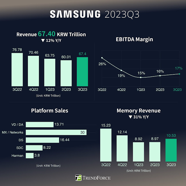
Samsung Electronics' financial results for 3Q23 highlighted a 12% QoQ revenue increase to 67.40 trillion Korean won, although there was a 12% YoY decrease. Notably, the company reported its highest quarterly profit for the year. Despite potential economic uncertainties in 2024, Samsung is optimistic about the recovery of the memory market and the rebound in smartphone demand. 

The memory sector saw a recovery compared to the previous quarter, especially in PC and mobile due to the rise in adoption of high-density DRAM and NAND products. The completion of customer inventory adjustments also played a role. Server demand was subdued for traditional servers due to macroeconomic uncertainties. However, strong demand persisted for AI-oriented high-density products. Samsung emphasized its focus on expanding sales of advanced node products like HBM DDR5, LPDDR5, and UFS 4.0. They also intend to manage high inventory products through production adjustments. The company expects the recovery trend in the memory market to accelerate further in the fourth quarter. Additionally, there has been a notable surge in HBM demand and the company is actively advancing its HBM businesses and plans to augment its HBM supply capacity by 2.5 times next year.


Trendforce on X (LINK)

The foundry division secured a record number of new orders, particularly in the HPC domain, despite a slow recovery in the mobile market. The new Taylor factory in Texas is set to begin production using the second-gen 3nm GAA process. The advanced packaging business has also been flourishing with orders from both domestic and international HPC clients.

Profits in the mobile panel business surged due to new flagship models from major clients. In contrast, the large panel business faced tepid demand. Samsung aims to cater to the growing mobile panel demand and increase profitability in the large panel sector by introducing new products and enhancing yield rates.

With the global economy expected to bounce back in 2024, the smartphone market's demand is anticipated to surge. High-end market growth is likely to continue, driven by the global recovery of the smartphone market.

Looking ahead to 2024, Samsung anticipates increased PC and mobile demand due to product replacement cycles initiated during the pandemic's early phase. High-density trends in both DRAM and NAND are expected to persist, propelled by on-device AI advancements. The company plans to focus on advanced node products, including 1B nanometer DDR5, LPDR5X, PCI Gen 5, and UFS 4.0, to bolster product competitiveness and profitability. Emphasizing the growing demand for generative AI, Samsung aims to strengthen its market position with high-density, low-power, and high-performance products for on-device AI, which has recently gained significant attention.

Sources;

TrendForce on X: "Samsung Electronics has released its financial results for 3Q23, reporting a quarterly revenue of 67.40 trillion Korean won—a 12% QoQ increase but 12% YoY decrease. The company achieved its highest quarterly profit of the year and anticipates that, despite ongoing global economic… https://t.co/RDKVjimgzN" / X (twitter.com)

Samsung Electronics Co Ltd (SSNLF) Q3 2023 Earnings Conference Call Transcript | Seeking Alpha


Wednesday, October 18, 2023

Micron Unveils Breakthrough NVDRAM: A Dual-Layer 32Gbit Non-Volatile Ferroelectric Memory with Near-DRAM Performance

At the upcoming International Electron Devices Meeting (IEDM), Micron is set to present a paper on a novel 32Gbit non-volatile ferroelectric memory, termed NVDRAM. Authored by Nirmal Ramaswamy, the vice president of advanced DRAM and emerging memory at Micron, the paper is titled "NVDRAm: A 32Gbit Dual Layer 3D Stacked Non-Volatile Ferroelectric Memory with Near-DRAM Performance for Demanding AI Workloads". It introduces the world’s first dual-layer, high-performance, 32Gbit stackable ferroelectric memory technology. This technology, branded as non-volatile dynamic random access memory (NVDRAM), promises faster data movement and better energy efficiency than traditional DRAM, making it ideal for larger neural network models.

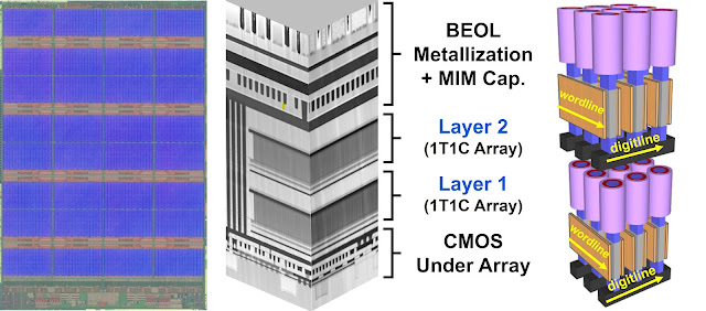
NVDRAM merges the benefits of ferroelectric memory cells – non-volatility and high endurance – with performance surpassing NAND flash memory retention and offering DRAM-like read/write speeds. The memory's architecture uses a 5.7nm ferroelectric capacitor for charge retention in a 1T1C DRAM structure, while dual-gated polycrystalline silicon transistors control access. The stacked double memory layer resides above a CMOS access circuit layer on a 48nm pitch. Despite the technological advancements, commercialization discussions remain speculative, potentially awaiting feedback from the IEDM presentation.


The images above show the final die layout (left) and SEM cross-section (center) of a 32Gb NVDRAM with 1T1C memory layers, fabricated over a CMOS array. On the right is a schematic diagram of NVDRAM memory arrays, showing polysilicon access device with orthogonal wordline (WL) and digitline (DL), and ferroelectric memory cells.

Abstract: Non-Volatile Ferroelectric w/DRAM-Like Performance, for AI & Machine Learning: Rapid growth in the size of the data models used in artificial intelligence (AI) and machine-learning (ML) applications is creating an urgent need for higher-bandwidth memory solutions. While new compute paradigms like near-memory-compute and processing-in-memory are being investigated, the best near-term opportunity is to outfit existing, traditional compute architectures with more efficient memory for faster data movement and to accommodate larger models. In this year’s Generative AI Focus Session, Micron researchers will unveil a memory technology for these uses which they call NVDRAM. It is the world’s first dual-layer, high-performance, high-density (32Gb), stackable and nonvolatile ferroelectric memory technology. It combines the non-volatile, high-endurance nature of ferroelectric memory cells with DRAM-like read/write speeds and endurance, and also surpasses the retention performance of NAND memory. NVDRAM uses an ultra-scaled (5.7nm) ferroelectric capacitor as the memory cell, and a dual-gated, stackable, polycrystalline silicon transistor as the access device. To achieve high memory density, two memory layers are fabricated above CMOS circuitry in a 48nm pitch, 4F2 architecture. Full package yield is demonstrated from -40°C to 95°C, along with reliability of 10 years (for both endurance and retention).

Sources:

Tuesday, September 26, 2023

TechInsights Discovers Micron's Cutting-Edge D1β LPDDR5 16 Gb DRAM Chips in Apple iPhone 15 Pro: Setting a New Standard in Memory Technology

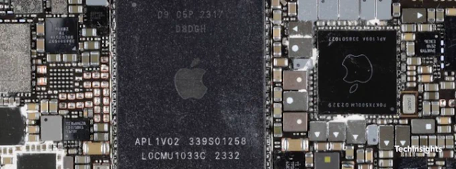
TechInsights has confirmed Micron's cutting-edge D1β LPDDR5 16 Gb DRAM chips in the Apple iPhone 15 Pro, marking the industry's first venture into the D1β generation. These chips are smaller and denser than their predecessors, showcasing significant advancements in DRAM technology. Notably, Micron has achieved this without utilizing Extreme Ultraviolet Lithography (EUVL), a technique employed by competitors like Samsung and SK Hynix for their DRAM processes. This achievement highlights Micron's dedication to pushing the boundaries of DRAM technology, emphasizing innovation and efficiency in the tech landscape. Micron's groundbreaking D1β LPDDR5 16 Gb DRAM chip promises to reshape the future of memory technology, setting a new standard for the industry.

(Source Micron.com)

1-BETA includes cool stuff

High-k/Metal Gate

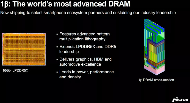
Micron's 1β fabrication process uses the company's 2nd generation high-K metal gate (HKMG) and is said to increase bit density of a 16Gb memory die by 35% as well as to improve power efficiency by 15% when compared to a similar DRAM device made on the company's 1α node

Pitch multiplication without the need for EUV Lithography

Micron's use of proprietary multi-patterning lithography involves advanced techniques for defining circuit patterns on semiconductor wafers with the highest precision. This approach allows Micron to create intricate patterns on the chips, achieving higher memory capacity in a smaller footprint. It enables the company to fit billions of memory cells on a chip that's roughly the size of a fingernail. 

While the semiconductor industry has been transitioning to extreme ultraviolet lithography (EUVL) to overcome technical challenges in patterning, Micron has opted for its multi-patterning lithography approach. This choice showcases Micron's expertise and innovation in lithography techniques, enabling them to continue shrinking circuit features and achieving greater memory capacity without relying on EUVL, which is still considered an emergent technology. 

By using proprietary multi-patterning lithography, Micron not only reduces the cost per bit of data but also enables devices with small form factors, such as smartphones and IoT devices, to incorporate more memory into compact spaces. This approach underscores Micron's commitment to staying at the forefront of memory technology innovation.
"While the industry has begun to shift to a new tool that uses extreme ultraviolet light to overcome these technical challenges, Micron has tapped into its proven leading-edge nano-manufacturing and lithography prowess to bypass this still emergent technology. Doing so involves applying the company’s proprietary, advanced multi-patterning techniques and immersion capabilities to pattern these minuscule features with the highest precision," Micron explains. Thy Tran, VP Process Integration, Micron


On the heels of the news that Micron has begun shipping QS-sample LPDDR5X components developed on the new 1-beta DRAM process node to its smartphone customers, host Jim Greene welcomes Thy Tran, Vice President of DRAM Process Integration, to the Chips Out Loud Podcast to discuss the emergent technology.

Sources:

Micron LPDDR5 16 Gb Non-EUVL Chip Found in Apple iPhone 15 Pro | TechInsights

LPDRAM | LPDDR | Micron Technology

Micron Ships World’s Most Advanced DRAM Technology With 1-Beta Node | Micron Technology


(Source: TechInsights.com)


Monday, September 25, 2023

NEO Semiconductor Unveils Revolutionary 3D NAND and DRAM Innovations at Flash Memory Summit 2023

NEO Semiconductor, known for its expertise in 3D NAND flash and DRAM technologies, presented groundbreaking innovations at Flash Memory Summit 2023 in August. The full presentation can be seen on Youtube (below). CEO Andy Hsu's keynote introduced their latest creation, 3D X-DRAM™, designed to overcome DRAM's capacity limitations and replace 2D DRAM. This technology utilizes the existing 3D NAND flash process with minor modifications, streamlining development and reducing costs. Hsu also unveiled a new AI application, "Local Computing," promising a substantial enhancement in AI chip performance.


X-DRAM™ significantly reduces data latency and provides ultra-high data throughput to unleash the full potential of High-Bandwidth Memory (HBM). HBM uses many Through Silicon Via (TSV) to increase I/O bandwidth. However, the HBM data latency remains almost the same when using conventional DRAM because bit line lengths remain the same.

Furthermore, NEO Semiconductor showcased various novel memory structures derived from 3D X-DRAM™, tailored for applications like 3D NOR flash memory, 3D Ferroelectric RAM (FFRAM), 3D Resistive RAM (RRAM), 3D Magnetoresistive RAM (MRAM), and 3D Phase Change Memory (PCM). These innovations enable the transition from 2D to 3D memory cells.


Hsu underscored the significance of these technologies for the semiconductor industry, cloud providers, and enterprises, highlighting that 3D X-DRAM™ offers a high-speed, high-density, cost-effective, and high-yield solution.

The presentation addressed the challenges faced by DRAM and NAND flash memory in the context of AI applications and introduced two innovative solutions – 3D X-DRAM™ and 3D X-NAND™.

Being part of the prestigious Flash Memory Summit, NEO Semiconductor showcased its technologies at booth number 215, and interested parties had the opportunity to schedule meetings with the company at the event.

In summary, NEO Semiconductor unveiled groundbreaking advancements in 3D NAND flash and DRAM technologies at Flash Memory Summit 2023, offering solutions to critical challenges in memory performance and capacity.

Source: NEO Semiconductor to Present Its Ground-Breaking 3D NAND and 3D DRAM Architectures in Keynote Address at Flash Memory Summit 2023 - Neo Semiconductor | X-Nand


Friday, May 7, 2021

Applied Materials MEMORY MASTER CLASS 2021 - slide deck

I missed this opportunity, however, I am grateful for Lita Shon-Roy just sending me the link to the slide deck - Tack så mycket. 

Slide deck for the Memory Class LINK

Next class up is Logic June 16, 2021 followed by more interesting topics in 2nd half 2021:

  • Specialty semiconductors
  • Heterogeneous design and advanced packaging
  • Inspection and process control

Teaser slide (Credit Dr. Sony Varghese, Director of Strategic Marketing at at Applied Materials)

You are welcome to contact us at TECHCET (jsundqvist@techcet.com) to dig further into the future surge of materials to realize the data-driven economy:

  • ALD/CVD precursors
  • Metals/PVD Targets
  • Photoresist
  • Wet chemicals
  • CMP pads & slurries
  • Bulk, Rare and Speciality gases
  • Wafers

Tuesday, February 9, 2021

Capacitorless DRAM using oxide semiconductors could be built in 3D layers above a processor’s silicon

One of the biggest problems in computing today is the “memory wall”—the difference between processing time and the time it takes to shuttle data over to the processor from separate DRAM memory chips. The increasingly popularity of AI applications has only made that problem more pronounced, because the huge networks that find faces, understand speech, and recommend consumer goods rarely fit in a processor’s on-board memory.

In December at IEEE International Electron Device Meeting (IEDM), separate research groups in the United States and in Belgium think a new kind of DRAM might be the solution. The new DRAM, made from oxide semiconductors and built in the layers above the processor, holds bits hundreds or thousands of times longer than commercial DRAM and could provide huge area and energy savings when running large neural nets, they say.


The transistors in the capacitorless DRAM developed by U.S.-based researchers includes a tungsten-doped indium oxide [orange] semiconductor, palladium top and bottom gates [yellow], nickel source and drain electrodes [green] and hafnium oxide dielectrics [blue]. Image: University of Notre Dame

Thursday, January 28, 2021

Micron Delivers Industry’s First 1α DRAM Technology

Micron recently announced that they are shipping memory chips built using the world’s most advanced DRAM process technology, which offers major improvements in bit density, power and performance. This is an astonishing feat of nanofabrication. 

Micron announcement: Micron Delivers Industry’s First 1α DRAM Technology

Micron’s 1α DRAM node will facilitate more power-efficient, reliable memory solutions and provide faster LPDDR5 operating speeds for mobile platforms that require best-in-class LPDRAM performance. Micron’s innovation brings the industry’s lowest-power mobile DRAM, with a 15% improvement in power savings,1 allowing 5G mobile users to perform more tasks on their smartphones without sacrificing battery life.

To find out more watch Thy Tran, vice president of DRAM Process Integration at Micron previously with Qimonda explain how to realize this amazing technology.


According to more details given in a Blog by Thy Tran, Micron uses Quadruple Patterning or Quad Patterning to realize the most critical lithography layers, which employ multiple ALD process steps and has become one of the biggest ALD market segment over recent years. See the video below by Lam Research for some more insights!


Quad patterning process flow (Image: Lam Research)


Wednesday, October 28, 2020

TechInsights Webinar: ALD/ALE Process in Commercially Available Memory Devices

2018 saw memory product manufacturers Samsung, Hynix, Toshiba and Micron introducing 64- or 72- stacked layer 3D-NAND devices, and move into 1x generation DRAM devices.

This presentation will examine some of the different structures we have seen through the evolution of these technologies, in particular the latest 3D-NAND and DRAM parts. We will also look at several historical applications of ALD/ALE technology that have been observed through reverse engineering. We will highlight the importance of ALD/ALE process in advanced logic devices. In many cases, the technology could not have advanced without the implementation of ALD technology.

Information and registration: LINK


Tuesday, July 2, 2019

Applied Materials to buy Japan's Kokusai to boost memory chip business and ALD

Here are more details and analyst responses on the Applied Materials Kokusai purchase and my own thoughts at the end:

(Reuters, LINK) - U.S. chip gear maker Applied Materials Inc (AMAT.O) on Monday agreed to buy Japanese peer Kokusai Electric for $2.2 billion from KKR & Co Inc (KKR.N), as it bets on rising demand for memory chips used in data centers, 5G phones, and AI-powered devices.  

In summary:
  • Kokusai is a small acquisition for Applied materials as compared to the previously failed mega-merger with Tokyo Electron, meaning that the road to approval should be easy. However, China’s willingness from a political standpoint is always a risk, Evercore analysts said. 
  • Apart from China, the acquisition will need approvals from Israel, Ireland, Japan, Korea and Taiwan, Applied Materials Chief Financial Officer Dan Durn said on a call with analysts.
  • Kokusai, which counts Samsung, SK Hynix, Toshiba and Micron among its top customers, reported revenue of $1.24 billion as of March 2018. 
  • Kokusai’s batch wafer processing tools are less technology intensive than Applied Materials’ single wafer tools, the recent focus on ultra-thin films has driven renewed interest in this group, DA Davidson analysts said.
So this whole purchase is really about Applied Materials getting a state of the art ALD technology for the memory business (DRAM and 3DNAND). The last readout is a bit crazy, the analyst refers to ALD as an "Ultra Thin Films". Anybody who has followed the ALD business the previous 15-20 years know that Applied Materials has repeatedly failed to take a big market share in ALD and that a Japanese Large Batch ALD reactor is one of the most advanced and reliable ALD tools out there - simply because nobody would like to trash a full load of +100 product wafers. The top three domination has been by:
  • ASM International
  • Tokyo Electron
  • Kokusai
The top 3 has been followed by Lam Research, Jusung Engineering, Wonik IPS and Applied Materials was always somewhere in this bunch. Even the inrodcution of the new Spatial ALD Olympia platform didn´t change things. It seems that Tokyo Electron took a large part of the spatial ALD market with their NT333 tool and ASM was able to defend their single wafer approach by making the XP platform super productive by adding more chamber slots (up to 16 for the latest ASM XP8 QCM).  

When it comes to IP in Spatial ALD, Tokyo Electron is No.1 followed by Applied Materials (see below).

IP Applications for spatial ALD

Magically, Kokusai settled the IP issues with ASM just before the Applied announcement (LINK). Historically, Kokusai has been masters in avoiding to call ALD ALD because of the IP situation. However, now there is a different situation and Kokusai also have single wafer ALD out there, and Applied is dominating the BEOL films deposition business so we can assume that Applied will enter top three and have a go at No 1. Exciting!

Wednesday, June 19, 2019

TechInsights’ Logic, NAND, DRAM and Emerging Memory Process Roadmaps are here

TechInsights’ Logic Process Roadmap offers an assessment and the anticipatory timing of new innovations from key players within the Logic space including: TSMC, Global Foundries, Intel & others. Download the roadmap here

TechInsights’ technology roadmaps show you the innovations we are monitoring

For over 30 years, TechInsights has been reverse engineering semiconductors and advanced technology products, developing the world’s largest library of technical analysis. We have built this library through two approaches: by conducting analysis in response to client requests, and by proactively analyzing disruptive or innovative technologies as they are released.

We constantly monitor the consumer electronics market to determine which manufacturers are planning to release new solutions, and when. We maintain and regularly update technology roadmaps in several different areas: Logic, NAND Flash Memory, DRAM, Emerging Memory, and Internet of Things Connectivity Systems on Chips, and more.

Updates to the roadmaps shown below are released throughout the year; check this page for updates. 

Thursday, November 22, 2018

UMass Engineers Make Crossbar Arrays of the Smallest Memristors

[University of Massachusetts Amherst LINK] AMHERST, Mass. – A research team at the University of Massachusetts Amherst says it has developed a promising building block for the next generation of nonvolatile random-access memory, artificial neural networks and bio-inspired computing systems.

  • "Memristor crossbar arrays with 6-nm half-pitch and 2-nm critical dimension" Nature Nanotechnology (2018) (LINK
  • Supplemenary information - including details on ALD processing (Al2O3 and HfO2) as well as all other processes (LINK)
 
2-nm memristor crossbar array [University of Massachusetts Amherst]
The team, led by Qiangfei Xia of the electrical and computer engineering department, says the memristor crossbar arrays they have built are, “to the best of our knowledge, the first high-density electronic circuits with individually addressable components scaled down to 2 nanometers dimension built with foundry-compatible fabrication technologies.” The results appear in the journal Nature Nanotechnology.

“This work will lead to high-density memristor arrays with low power consumption for both memory and unconventional computing applications,” says Xia. “The working circuits have been made with technologies that are widely used to build a computer chip.”

Understanding the scale of this work is important, Xia says. One nanometer (nm) is one billionth of a meter. The diameter of a human hair is about 100 micrometers, or 100,000 nanometers. Two nanometers are just a few atoms wide. A crossbar is a matrix of tiny switches.

In the Nature Nanotechnology paper, Xia’s research team explains that organizing small memristors into high-density crossbar arrays is critical to meet the ever-growing demands in high-capacity and low-energy consumption, but is challenging because of difficulties in making highly ordered and highly conductive nanoelectrode arrays. The team has addressed this challenge by developing “nanofins,” metallic nanostructures with very high height-to-width ratio and hence vastly reduced resistance, as the electrodes.

This research is an outgrowth of Xia’s 2013, five-year, $400,000 grant from the National Science Foundation (NSF) Faculty Early Career Development (CAREER) Program to develop emerging nanoelectronic devices. Xia’s NSF research has been addressing the biggest obstacle for the continued operation of Moore’s Law, which states that the number of transistors on integrated circuits doubles approximately every two years.

“It (Moore’s Law) worked perfectly for more than 40 years, but now we’re reaching its fundamental limit, due to the quantum effects related to electron flow,” says Xia. “So, we absolutely need new devices that can do a better job.” In addition to Xia, the other authors of the Nature Nanotechnology paper are Shuang Pi, Can Li, Hao Jiang, Weiwei Xia, Joshua Yang and Huolin Xin

Tuesday, November 13, 2018

Spin Memory Teams With Applied Materials to Produce a Comprehensive Embedded MRAM Solution

FREMONT, Calif. — Spin Memory, Inc. (Spin Memory), the leading MRAM developer, today announced a commercial agreement with Applied Materials, Inc. (Applied) to create a comprehensive embedded MRAM solution. The solution brings together Applied’s industry-leading deposition and etch capabilities with Spin Memory’s MRAM process IP.


Key elements of the offering include Applied innovations in PVD and etch process technology, Spin Memory’s revolutionary Precessional Spin CurrentTM (PSCTM) structure (also known as the Spin Polarizer), and industry-leading perpendicular magnetic tunnel junction (pMTJ) technology from both companies. The solution is designed to allow customers to quickly bring up an embedded MRAM manufacturing module and start producing world-class MRAM-enabled products for both non-volatile (flash-like) and SRAM-replacement applications. Spin Memory intends to make the solution commercially available from 2019.

“In the AI and IoT era, the industry needs high-speed, area-efficient non-volatile memory like never before,” said Tom Sparkman, CEO at Spin Memory. “Through our collaboration with Applied Materials, we will bring the next generation of STT-MRAM to market and address this growing need for alternative memory solutions.”

“Our industry is driving a new wave of computing that will result in billions of sensors and a dramatic increase in data generation,” said Steve Ghanayem, senior vice president of New Markets and Alliances at Applied Materials. “As a result, we are seeing a renaissance in hardware innovation, from materials to systems, and we are excited to be teaming up with Spin Memory to help accelerate the availability of a new memory.”
About the PSC

Saturday, March 24, 2018

ASM International report recovery in the single-wafer ALD market due to strong 3D-NAND fab invest

Almere, The Netherlands, March 22, 2018 ASM International N.V. (Euronext Amsterdam: ASM) today publishes its 2017 Annual Report.

ASMI's Annual Report is also available on the company's website www.asm.com. The Annual Report includes the Corporate Responsibility Report and the Remuneration Report in order to increase the relevancy and quality of reporting to all stakeholders.

ASMI will hold its Annual General Meeting of Shareholders (AGM) on May 28, 2018. The AGM agenda with all related documents will be available in due time.

MESSAGE FROM THE CEO (asm.com LINK)
In 2017 we achieved significant progress against our strategic targets. Our sales benefited from a clear recovery in the single-wafer Atomic Layer Deposition (ALD) market, in particular driven by strong increases in the 3D-NAND segment. During the year we also successfully expanded our position in the epitaxy market with an important tool win from a leading foundry customer. In total, our revenue increased by 23% to a new record level. 


Please check out the financial data at a glance here (LINK).

Saturday, January 27, 2018

Scaling proven for embedded Super Fast Non-volatile Memory from Dresden

Ferroelectric hafnium oxide and related materials have been developed in Dresden, Germany for over 10 years now. At the IEDM2017 in December Globalfoundries Fab1 and their partners (NaMLab, Fraunhofer and Ferroelectric Memory GmbH) presented their latest results using the Fab1 22nm FDSOI technology with embedded NVM cells embedded as adopted "standard" high-k / metal gate stacks in the front end process module as so called FeFETs.

Previously much of the work was based on Globalfoundries Fab1 28 nm technology so the move to 22 nm really proves that scalig is back to ferroelectric memory technologies as shown on LinkedIn by Prof. Mikolajick (NaMLab) below.. Since the high-k (doped HfO2) is deposited by ALD this technology is scalable also for FinFETs so don´t be surprised if Globalfoundries would soon present also FeFinFETs.

A FeFET based super-low-power ultra-fast embedded NVM technology for 22nm FDSOI and beyond

IEEE Xplore: 25 January 2018 DOI: 10.1109/IEDM.2017.8268425  

Abstract: We show the implementation of a ferroelectric field effect transistor (FeFET) based eNVM solution into a leading edge 22nm FDSOI CMOS technology. Memory windows of 1.5 V are demonstrated in aggressively scaled FeFET cells with an area as small as 0.025 μm2 At this point program/erase endurance cycles up to 105 are supported. Complex pattern are written into 32 MBit arrays using ultrafast program/erase pulses in a 10 ns range at 4.2 V. High temperature retention up to 300 °C is achieved. It makes FeFET based eNVM a viable choice for overall low-cost and low-power IoT applications in 22nm and beyond technology nodes.


Friday, January 5, 2018

Memory chips led the way in 2017 boosting a 22% record semiconductor growth in revenue

Memory chips (DRAM & FLASH) led the way in 2017 boosting a 22% record semiconductor growth in revenue. Samsung Electronics became the number 1 in overall semiconductor sales for the first time, displacing Intel, which had held the top spot in sales every year since 1992. 


EE Times reports : Semiconductor sales grew by 22 percent to reach a record $419.7 billion — with memory chips leading the way — according to a preliminary estimate by market research firm Gartner.

Gartner (Stamford, Conn.) estimates that increased sales of memory chips due to shortages of NAND flash and DRAM accounted for about two-thirds of overall chip market growth in 2017. Memory also become the single largest semiconductor products category last year, according to the firm.

Full story: LINK


Gartener 2016 to 2017 revenue change for Top 10 Semiconductor companies [replotted]

Thursday, August 3, 2017

Challenges in 3D-NAND high volume manufacturing

Planar NAND was scaled and at the end limited by the cost of lithography, wheras 3D NAND scaling is enabled by advanced deposition and etch processes defining complex high aspect ratio 3D structures. Here is an excellent article by Lam Research in Solid State Technology on the challenges in 3D-NAND fabrication.

Solis State Technology : LINK

Screen capture from Solid State Technology online magazine (LINK)

Wednesday, June 7, 2017

Another breakthrough in CMOS-compatible ferroelectric memory

Imec, the world-leading research and innovation hub in nanoelectronics and digital technology, announced today at the 2017 Symposia on VLSI Technology and Circuits the world's first demonstration of a vertically stacked ferroelectric Al doped HfO2 device for NAND applications. Using a new material and a novel architecture, imec has created a non-volatile memory concept with attractive characteristics for power consumption, switching speed, scalability and retention. The achievement shows that ferro-electric memory is a highly promising technology at various points in the memory hierarchy, and as a new technology for storage class memory. Imec will further develop the concept in collaboration with the world's leading producers of memory ICs.

Full story : LINK

Friday, December 2, 2016

ASM International technical luncheon seminar in San Francisco at IEDM 2017, December 7

ASM International N.V. (Euronext Amsterdam: ASM) today announces that it will host a technical luncheon seminar in San Francisco, CA, US, on Wednesday, December 7, 2016, the third day of the IEDM Conference.


At this technology seminar ASM will highlight the challenges and potential solutions for achieving next generation 3D devices.

The agenda is as follows:

11:30 am Food and drinks

12:00 - 12:05 pm Ivo Raaijmakers (ASM) - Welcome and introduction

12:05 - 12:30 pm Invited speaker: Raghuveer Makala (SanDisk/WDC) - "Thin film deposition
challenges for 3D NAND"

12:30 - 12:55 pm Invited speaker: Jorge Kittl (Samsung) - "Perspectives on logic scaling and
implications for process requirements"

Following the presentations, there is an opportunity for open discussion and networking until 1:15 pm.

The ASM technology seminar will take place in the Golden Gate room (25th floor) at the Nikko Hotel (across from the Hilton San Francisco), San Francisco, CA 94102. The room will open at 11:30 am for invited attendees. Interested parties should contact Rosanne de Vries, +31 88 100 8569, rosanne.de.vries@asm.com.

Wednesday, October 12, 2016

HP reports low energy Memristor precisely tuned by ALD

Nanotechweb reports: Researchers at Hewlett Packard Labs in California, the University of Massachusetts Amherst and Seoul National University are reporting on a new low-current, self-rectifying memristor made from titanium ion electron traps in a niobium oxide matrix. The device might be used as an embedded memory on low-power chips and for storing data in Internet of Things (IoT) appliances.
 
 
The memristor device (Pt/NbOx/TiOy/NbOx/TiN) is based on titanium ion electron traps in a niobium oxide (NbOx) matrix deposited by ALD. ALD allows control of the sub-atomic monolayers in the structure and so precisely control how the Ti traps are distributed in the NbOx matrix. (Figure from Nanotechweb.org)
 
According to the team, led by Stanley Williams, also of Hewlett Packard Labs, the new memristor could be used to make embedded memories for low-power chips, such as ASICS. “Since the technology is fully CMOS compatible, it might also be used to store data in or near sensors at the edge of IoT devices,” says Kim. “Eventually, it might find use as a stand-alone non-volatile memory for low-power systems.”

Monday, September 26, 2016

RASIRC® BRUTE® peroxide and hydrazine technology for leading edge memory and high performance logic

Hydrogen peroxide (H2O2) gas is an oxidant that improves passivation and nucleation density at semiconductor interfaces, potentially leading to reduced interfacial defect density. A new technology capable of generating and delivering stable anhydrous H2O2 gas has been developed by RASIRC. The method utilizes a substantially anhydrous H2O2 solution, a carrier gas and membrane pervaporator in order to deliver anhydrous H2O2. A broad range of high-k materials and interfaces that can be improved as well as enhanced transistor performance were shown at ALD2016 Ireland. 
H2O2 allows for unique process windows in ALD due to its oxidative potential, which lies between more commonly used water and ozone, and greater acidity relative to water [1]

RASIRC BRUTE H2O2 Apparatus (H2O2 + solvent) surrounds the Nafion membrane tubes. H2O2 passes through the membrane walls and is picked up by the carrier gas.

Growth of many different films has been showcased with BRUTE Peroxide and the related RASIRC product BRUTE Hydrazine. In presentations and posters at ALD2016 Ireland the RASIRC line of BRUTE Hydrazine and BRUTE Peroxide showed impressively many useful results by many different precursors. In total, four separate posters and presentations covered growth passivation of SiOx on SiGe, SiNx on SiGe, SiON on SiGe as well as  growing HfO2, ZrO2, TiO2, Al2O3 and  TaOx with the BRUTE line of new reactive chemistries.

Transistor channel passivation, Dan Alvarez presented results of growing SiNx and SiOxNx  on SiGe using BRUTE Hydrazine and BRUTE Peroxide [2]. These films were then further processed with HfO2 dielectric layer to grow MOSCAPs. These MOSCAPS had better performance than those processed with HF last and water vapor, where improved defect density and lower leakage characteristics were reported. In addition, the presentation by Dan Alvarez discussed how anhydrous hydrazine can be used to create a thin layer of silicon nitride that can act as a diffusion barrier or channel passivation layer prior to dielectric deposition in FinFets or MOSFETs. The study focused on <400 °C silicon nitride ALD process and showed how further oxidation using anhydrous peroxide provides good nucleation for High-k deposition.

A low Temperature Passivation on SiGe(110) via plasma free process by subsequent doses of anhydrous hydrazine and hexachlorodisilane can further increase the amount of SiNx on the surface. A final treatment with HOOH can prepare the surface for high-k deposition.

BRUTE Peroxide was reported to reduce HfO2 gate oxide EOT by reduction in the interface layer

Steve Consiglio from Tokyo Electron, presented data comparing growth of HfO2 and interface layer thickness control [3]. Utilizing 300 mm Si wafers with pre-formed chemical oxide, he evaluated an all in-situ method of chemical oxide removal (COR; Si-H termination) followed by H2O2(g) dosing prior to ALD growth of HfO2 using TEMAHf and H2O. The study reported faster growth rate with H2O2 than for O3. Most interestingly, the interface results were very exciting with interface layer regrowth in the 2-4 Ångstrom range, which corresponds to ½ to 1 monolayer of SiOx interface for improved EOT and this was definitely much thinner than the results reported using O3.
Aluminum oxide, Al2O3 ALD has been presented previously [4]. This time RASIRC had a poster on improved nucleation by using H2O2 as an oxidant in ALD of Al2O3 [5]. The poster explained the need for a novel oxidant that improves passivation and nucleation density at semiconductor interfaces. The study was performed on SiGe(110) surfaces and  provides a direct comparison of equal amounts of water, 30% H2O2/H2O, and anhydrous H2O2. A five-fold increase was found in nucleation density for H2O2 versus water, and a three-fold increase for H2O2 versus 30% H2O2/H2O. An additional comparison was made of H2O2 to H2O by deposition of Al2O3 on an Si-H surface. This comparison found denser nucleation and faster initiation for H2O2 treated surfaces.


In a direct comparison of TMA based ALD with water vs peroxide the coverages of O and Al are higher with peroxide and growth starts earlier.

Zirconium oxide, ZrO2  was presented in study by Intermolecular and RASIRC at ALD2016 Poster session [6]. By utilizing the Intermolecular Combinatorial ALD platform equipped with a RASIRC BRUTE H2O2 apparatus the study compared the performance of H2O2 against O3 in a zirconium oxide ALD using ZyALD Air Liquide industry standard Zr-precursor. By MIMCAP integration the differences in ZrOx unit film properties and electrical performance was shown. Similar unit film behavior (GPC, linearity, growth saturation, film crystallinity etc.) was observed between O3 and H2O2.


Oxidant dosing (left) show that 4% O3 yields saturated response, whereas H2O2 and 20% O3 display softer saturation. ZyALD dose (middle) for each oxidant system shows definite completion for 20% O3. All three investigated conditions show linear growth without growth inhibition (right).       


The MIMCAP study (above) concluded that ZrO2 produced with H2O2 matched the best performance of 4% O3. Therefore it is possible to avoid issues observed with high (20%) O3 concentration as showcased in the figure below. More importantly, H2O2 has the capability to produce thin node dielectric, which is needed for highly scaled DRAM nodes.

Optical (left) and SEM (middle) images of MIMCAPs, post-annealing, with defects observed with 20% O3 and thin 5 nm ZrOx. As comparison blanket TiN film enhanced resistivity was observed (right) using 4 resp. 20% O3 concentrations, whereas H2O2 lays in-between. Results suggest that elevated TiN bottom electrode oxidation takes place with 20% O3 that leads to degassing during annealing.  However, the defect can be avoided with minimal reduction in growth rate, by using H2O2 as the oxidant.
Hafnium oxide, HfO2 by TDMAHf along TEMAHf was the first Hf-precursors in use at the introduction of High-k in the DRAM industry more than 10 years ago at the 90nm node. HfO2 ALD has also been investigated by Intermolecular using the H2O2/TDMAHf ALD process and in this study the MIMCAPs showed to match the best O3 performance like in the case of ZrO2 given in more detail above. In addition, Tokyo Electron presented work for HfO2 as summarized above.  
Titanium oxide, TiO2 low temperature (100 °C) TiOx ALD using H2O2 and TiMCTA (methylcyclopentadienyl tris(dimethylamino)titanium) as the metal precursor has successfully been grown as also reported by Intermolecular at ALD2016 Poster session [6].  
   
To summarize, RASIRC and their collaborations throughout the semiconductor insdustry and with leading research facilities have shown that many different films can be grown with BRUTE Peroxide and BRUTE Hydrazine and most importantly that BRUTE Peroxide can reduce EOT by reduction in the interface layer, yielding higher performing memory and logic devices.
References
[1] D. R. Lide, CRC Handbook of Chemistry and Physics (CRC Press, Boca Raton, 1996).
[2] Hydrogen peroxide gas for improved nucleation and initiation in ALD, Daniel Alvarez, Adam Hinckley, Pablo Macheno, Christopher Ramos, Jeffrey Spiegelman,
Anthony Muscat, Presentation at ALD 2016 Ireland.
[3] Anhydrous H2O2 for ALD HfO2 growth and interfacial layer thickness control, Steven Consiglio, Robert Clark, Takahiro Hakamata, Kandabara Tapily, Cory Wajda, Gert Leusink, Presentation at ALD2016 Ireland.
[4] Comparison of Water Vapor to Ozone for Growth ALD Films, J. Spiegelman, J. Sundqvist, EU PVSEC Proceedings 2011, page 1694 – 1698.
[5] Hydrogen peroxide gas for improved nucleation and initiation in ALD, Daniel Alvarez, Adam Hinckley, Pablo Macheno, Christopher Ramos, Jeffrey Spiegelman, Anthony Muscat, Poster ALD2016 Ireland.
[6] Comparison of hydrogen peroxide and ozone for use in zirconium oxide atomic layer deposition, Gregory  Nowling,  Stephen Weeks, Daniel Alvarez, Mark Leo, Jeff Spiegelman, Karl Littau, Poster ALD2016 Ireland.