Friday, December 25, 2015

Self-assembled block copolymer template and ALD from Israel University of Technology

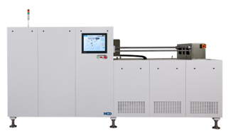
Here is a cool paper from from Prof. Gitti Frey and Moshe Moshonov at Technion, Israel Institute of Technology, Haifa Israel on Self-assembled block copolymer template and ALD. This is a rather hot topic for future nano patterning. They are using an ALD reactor that I did not come across until now - a MVD100E Applied MST system with an integrated oxygen plasma module to do ALD of ZnO into the organic films and self assembly of Block Copolymers.


The MVD100E Applied MST is a 200 mm tool capable of Molecular Vapor Deposition (MVD) and ALD for R&D or pilot manufacturing. It is designed for high performance, flexibility and reliability for the most demanding applications. Corporate and Academic Research Labs have called it their most versatile and reliable piece of equipment (http://www.appliedmst.com/mvd-100e/)

Here is also a video that I found on Youtube on how to operate the MVD100E tool from The Integrated Nanosystems Research Facility at The University of California, Irvine (INRF UCI).


Directing Hybrid Structures by Combining Self-Assembly of Functional Block Copolymers and Atomic Layer Deposition: A Demonstration on Hybrid Photovoltaics

Moshe Moshonov and Gitti L. Frey
Langmuir, 2015, 31 (46), pp 12762–12769 DOI: 10.1021/acs.langmuir.5b03282


The simplicity and versatility of block copolymer self-assembly offers their use as templates for nano- and meso-structured materials. However, in most cases, the material processing requires multiple steps, and the block copolymer is a sacrificial building block. Here, we combine a self-assembled block copolymer template and atomic layer deposition (ALD) of a metal oxide to generate functional hybrid films in a simple process with no etching or burning steps. This approach is demonstrated by using the crystallization-induced self-assembly of a rod–coil block copolymer, P3HT-b-PEO, and the ALD of ZnO. The block copolymer self-assembles into fibrils, ∼ 20 nm in diameter and microns long, with crystalline P3HT cores and amorphous PEO corona. The affinity of the ALD precursors to the PEO corona directs the exclusive deposition of crystalline ZnO within the PEO domains. The obtained hybrid structure possesses the properties desired for photovoltaic films: donor–acceptor continuous nanoscale interpenetrated networks. Therefore, we integrated the films into single-layer hybrid photovoltaics devices, thus demonstrating that combining self-assembly of functional block copolymers and ALD is a simple approach to direct desired complex hybrid morphologies.

Wednesday, December 23, 2015

ETH Zurich prints the tiniest inkjet color picture of the world

ETH Zurich reports: Researchers of ETH Zurich and ETH start-up company Scrona achieve a new world record! They have printed a color picture depicting clown fishes around their sea anemone home. This picture is as tiny as the cross-sectional area of a human hair.


The tiniest inkjet color picture of the world is as small as the cross-sectional area of a human hair or a single pixel of a retina display. (Photograph: Scrona/ETH Zurich)

Full story: https://www.ethz.ch/en/news-and-events/eth-news/news/2015/12/tiniest-color-picture-ever-printed.html

Dancing water molecules at the SrO on surface of ruthenates

Here is a very recent publication from TU Wien in Nature on adsorption of H2O molecules on a SrO surface of strontium ruthenate that should be very interesting for all ALD guys working with this process and material for e.g. MIM Capacitors. There is also a recent highlight of the publication in EurekAlert! http://www.eurekalert.org/pub_releases/2015-12/vuot-sph122115.php


This is a visualization of a dancing H2O molecule dissociating on the SrO crystal surface. (EurekAlert!, Credit : TU Wien)

EurekAlert! reports: "We studied strontium ruthenate - a typical perovskite material," says Ulrike Diebold. It has a crystalline structure containing oxygen, strontium and ruthenium. When the crystal is broken apart, the outermost layer consists of only strontium and oxygen atoms; the ruthenium is located underneath, surrounded by oxygen atoms.

A water molecule that lands on this surface splits into two parts: A hydrogen atom is stripped off the molecule and attaches to an oxygen atom on the crystal's surface. This process is known as dissociation. However, although they are physically separated, the pieces continue to interact through a weak "hydrogen bond".

It is this interaction that causes a strange effect: The OH group cannot move freely, and circles the hydrogen atom like a dancer spinning on a pole. Although this is the first observation of such behaviour, it was not entirely unexpected: "This effect was predicted a few years ago based on theoretical calculations, and we have finally confirmed it with our experiments" said Diebold

Adsorption of water at the SrO surface of ruthenates

Daniel Halwidl, Bernhard Stöger, Wernfried Mayr-Schmölzer, Jiri Pavelec, David Fobes, Jin Peng, Zhiqiang Mao, Gareth S. Parkinson, Michael Schmid, Florian Mittendorfer, Josef Redinger & Ulrike Diebold 
Nature Materials Published online, , doi:10.1038/nmat4512

Although perovskite oxides hold promise in applications ranging from solid oxide fuel cells to catalysts, their surface chemistry is poorly understood at the molecular level. Here we follow the formation of the first monolayer of water at the (001) surfaces of Srn+1RunO3n+1 (n = 1, 2) using low-temperature scanning tunnelling microscopy, X-ray photoelectron spectroscopy, and density functional theory. These layered perovskites cleave between neighbouring SrO planes, yielding almost ideal, rocksalt-like surfaces. An adsorbed monomer dissociates and forms a pair of hydroxide ions. The OH stemming from the original molecule stays trapped at Sr–Sr bridge positions, circling the surface OH with a measured activation energy of 187 ± 10meV. At higher coverage, dimers of dissociated water assemble into one-dimensional chains and form a percolating network where water adsorbs molecularly in the gaps. Our work shows the limitations of applying surface chemistry concepts derived for binary rocksalt oxides to perovskites.


3774700967338

Tuesday, December 22, 2015

A fresh review in Advanced Materials on ALD modelling

Here is a fresh review in Advanced Materials on ALD modelling from Simon Elliott and co-workers at Tyndall National Institute University College Cork. It contains an rather interesting part on MLD/ALD combination.

The article lists the following four major challenges for modelling ALD:
  1. Computing Precursor Volatility
  2. The Effect of Weak Interactions on Adsorption
  3. Modeling Plasma-Enhanced ALD
  4. Simulating Processes Over Long Time Scales

Modeling Mechanism and Growth Reactions for New Nanofabrication Processes by Atomic Layer Deposition

Simon D. Elliott, Gangotri Dey, Yasheng Maimaiti, Hayrensa Ablat, Ekaterina A. Filatova1 and Glen N. Fomengia
Article first published online: 21 DEC 2015
DOI: 10.1002/adma.201504043


Recent progress in the simulation of the chemistry of atomic layer deposition (ALD) is presented for technologically important materials such as alumina, silica, and copper metal. Self-limiting chemisorption of precursors onto substrates is studied using density functional theory so as to determine reaction pathways and aid process development. The main challenges for the future of ALD modeling are outlined.


Queen Elisabeth investigating The Tyndall Effect sporting a clean room hat and Class 100 stealth clean room gloves at a visit to Tyndall Institute, University College Cork in 2011.


Monday, December 21, 2015

New CNT based device from MIT that catches hard to detect molecules

MIT News Reports: Engineers at MIT have devised a new technique for trapping hard-to-detect molecules, using forests of carbon nanotubes. The team modified a simple microfluidic channel with an array of vertically aligned carbon nanotubes — rolled lattices of carbon atoms that resemble tiny tubes of chicken wire. The researchers had previously devised a method for standing carbon nanotubes on their ends, like trees in a forest. With this method, they created a three-dimensional array of permeable carbon nanotubes within a microfluidic device, through which fluid can flow. Now, in a study published this week in the Journal of Microengineering and Nanotechnology, the researchers have given the nanotube array the ability to trap certain particles. To do this, the team coated the array, layer by layer, with polymers of alternating electric charge.


A patterned and cylindrical structure made up of carbon nanotubes. (Courtesy of the researchers, MIT)


A zoomed in view of carbon nanotubes, showing individual tubes. (Courtesy of the researchers, MIT) 

Picosun is bringing ALD technology to Outer Space

Spaceworthy encapsulants from Picosun

Picosun Oy, leading supplier of highest quality Atomic Layer Deposition (ALD) thin film coating solutions for industrial manufacturing, successfully applies ALD technology to protect sensitive electronic components against harsh environmental conditions.


ALD oxide nanolaminates developed by Picosun have been proven to efficiently protect printed circuit board (PCB) components from aging effects such as corrosion and tin whisker formation. Corrosion typically occurs on the interface between the board and the component. Gaps in the solder tin covering the sharp edges of the component’s conducting pins may leave them vulnerable against environmental factors such as humidity, liquid and gaseous impurities. This is particularly detrimental in several high end applications where unfaltering component performance is required, such as in aerospace electronics. ALD forms ultra-thin, hermetic, inert, flexible, and protective film over the whole board, isolating even the most sensitive points from the ambient conditions. Due to the nanometer-scale thickness, the ALD film has negligible impact on the PCB functionality.

“Production-scale processing of PCBs requires production-optimized ALD technology. Picosun has unmatched and the most comprehensive expertise in providing large scale ALD solutions to various industries, not only to semiconductor and IC manufacturing but also for protection of 3D items – coins, watch and jewelry parts, and medical implants being just a few examples. Expanding our business to PCB encapsulation is yet another example of ALD’s penetration throughout the spectrum of today’s industrial manufacturing”, states Juhana Kostamo, Managing Director of Picosun. 

The Picosun-ESA contract is a part of an activity funded by the ESA programmes European Component Initiative Phase 4 and Strategic Initiative. Disclaimer: The views expressed herein can in no way be taken to reflect the official opinion of the European Space Agency.

Sunday, December 20, 2015

ALD is Global - Blog visitors All Time

As you can imagine ALD has a global interest and it is always existing to follow which countries that make it to the top 10 on a weekly basis.


This week we have The UK and Taiwan making it to the top 10 kicking out Sweden and The Netherlands. Above is the overall visitor statistics since the start. US is for sure still in the lead and France has taken up a new No.2 position pushing down Germany one down - Vive la France! Interestingly there was 5 visitors from Brazil today.

Here are some of the most popular posts in December - as you can see it is the leading edge stuff people enjoy reading about.


Essay on the history of ALD - Molecular Layering

As Riikka just announced - Now it is here the Essay on the history of creation and development of the molecular layering technique (ML) and later known as atomic layer deposition (ALD). We´re collecting contributions to make it an Open Access and are short of $1,000 of the total $3,000 needed - please contact either me or Riikka Puurunen if you would like to contribute!


Prof. V.B. Aleskovskii and his student S.I. Kol’tsov

From V. B. Aleskovskii's “Framework” Hypothesis to the Method of Molecular Layering/Atomic Layer Deposition

Anatolii A. Malygin, Victor E. Drozd, Anatolii A. Malkov and Vladimir M. Smirnov

Chemical Vapor Deposition, Volume 21, Issue 10-11-12, pages 216–240, December 2015,
DOI: 10.1002/cvde.201502013

Abstract: This essay is dedicated to the history of creation and development of the molecular layering technique (ML) which, in the modern community of non-Russian scientists, is commonly referred to as atomic layer deposition (ALD). Basic research in the field of chemical transformations of solid surfaces using the ML method in the light of the “framework” hypothesis proposed by V. B. Aleskovskii in 1952 is discussed. A number of questions raised by international scientists including those involved in the Virtual Project on the History of ALD (VPHA, 2013), and scientists from conferences in Helsinki (Finland, May 2014.), Kyoto (Japan, June 2014), and personal communications amongst peers are addressed. For the first time in English, this article provides information about V. B. Aleskovskii and S. I. Kol'tsov who are closely associated with development of the ML technique in the Soviet Union. This paper also informs the scientific community about research groups currently engaged in ML research in Russia and introduces the scientific school of “Chemistry of highly organized substances”, founded and supervised by V. B. Aleskovskii.
 
The authors express their deep gratitude to all the colleagues who initiated the writing of this review, particularly R. Puurunen and A. Abdulagatov. Special thanks to A. Abdulagatov for his valuable suggestions that helped strengthen the content of this article. The topic suggestions that have been sent to us by our colleagues from different countries have allowed us to more clearly define the structure and content of this article and we have tried our best to cover them all in detail. Great thanks to Puurunen Riikka (Finland), Sundqvist Jonas (Sweden), Pedersen Henrik (Sweden), Koshtyal Yury (Russia), van Ommen, J. Ruud, (the Netherlands). We would like to acknowledge the Russian science Foundation for partial financial support (contract No. 14-13-00597).

Saturday, December 19, 2015

How to ALD in Metal-Organic Framworks (MOFs) using Ultratech/CNT Savannah

Here is a fresh open source publication on a rather hot topic - using ALD in Metal-Organic Framworks (MOFs). It is really a fantastic publication giving step by step detailed instructions how to perform the materials synthesis. The researchers come from Northwestern University, Argonne National Laboratory and King Abdulaziz University. They are using ALD to deposit into the extremely well defined porous material. The ALD processing is performed in the popular Ultratech/Cambridge Nanotech Savannah reactor using a grid powder holder (see description below). Some of the researchers are involved in a startup company, NuMat Technologies, which is seeking to commercialize metal-organic frameworks.

 
Background:  MOFs are a class of crystalline materials that have a well-defined and atomically precise structures, exceptional porosities and the tunability of : 
  • particle size
  • pore size
  • surface area
  • density
  • topology
  • molecular affinity 
Beacuse of these exceptional properties MOFs are being investigated for a broad range of applications like: 
  • gas storage 
  • gas separation
  • heterogeneous catalysis
  • sensing
  • light harvesting
  • drug delivey 
Please check for all the details in the open-source publication below and real all the details:

Scalable synthesis and post-modification of a mesoporous metal-organic framework called NU-1000

Timothy C Wang,    Nicolaas A Vermeulen, In Soo Kim, Alex B F Martinson, J Fraser Stoddart, Joseph T Hupp & Omar K Farha  

Nature Protocols, 11, 149–162 (2016) doi:10.1038/nprot.2016.001

The synthesis of NU-1000, a highly robust mesoporous (containing pores >2 nm) metal-organic framework (MOF), can be conducted efficiently on a multigram scale from inexpensive starting materials. Tetrabromopyrene and (4-(ethoxycarbonyl)phenyl)boronic acid can easily be coupled to prepare the requisite organic strut with four metal-binding sites in the form of four carboxylic acids, while zirconyl chloride octahydrate is used as a precursor for the well-defined metal oxide clusters. NU-1000 has been reported as an excellent candidate for the separation of gases, and it is a versatile scaffold for heterogeneous catalysis. In particular, it is ideal for the catalytic deactivation of nerve agents, and it shows great promise as a new generic platform for a wide range of applications. Multiple post-synthetic modification protocols have been developed using NU-1000 as the parent material, making it a potentially useful scaffold for several catalytic applications. The procedure for the preparation of NU-1000 can be scaled up reliably, and it is suitable for the production of 50 g of the tetracarboxylic acid containing organic linker and 200 mg–2.5 g of NU-1000. The entire synthesis is performed without purification by column chromatography and can be completed within 10 d.


Structure of NU-1000 and developed post-synthetic modification methods on this platform. The blue, red and black spheres represent zirconium, oxygen and carbon, respectively. The perfluoro alkane SALIed into NU-1000 is represented in green, and the gold sphere shows the location of a metal cluster introduced into NU-1000 using AIM. [doi:10.1038/nprot.2016.001 Nature Publishing Group, Licence number 3772371203825]


Equipment setup for 250-mg-scale AIM modification for Al-AIM. (a,b) The metal screen constituting the power holder (a) and the reaction chamber of the ALD instrument (b). 
[doi:10.1038/nprot.2016.001 Nature Publishing Group, Licence number 3772371203825]


Friday, December 18, 2015

European researchers reach graphene production breakthrough, under project GRAFOL

Graphene-info reports: Researchers involved in the €10.6 million European research project called GRAFOL have reportedly demonstrated a cost-effective roll-to-roll production tool capable of making large sheets of graphene on an industrial scale. The tool operates at atmospheric pressure and at reduced operating temperature, and is proclaimed by the researchers "the best route to low-cost manufacture".


Graphene-enhanced perovskite PV (Graphene-info)

SAMCO Signs Distributor Contract with Swedish SiC CVD OEM

On December 1, 2015, SAMCO Inc. signed an international distributor agreement with Epiluvac AB, a Swedish manufacturer of silicon carbide (SiC) CVD systems. The agreement terms grant SAMCO exclusive distribution rights in Japan, Taiwan, Singapore, Malaysia and the Philippines.


Visit Epiluvac: http://epiluvac.com/

As a global enterprise, SAMCO is marketing its dry etching and various CVD systems in Asia, Europe and North America in addition to gaining market share within Japan. SAMCO's dry etching and plasma CVD technology serves applications involving wide band-gap semiconductor materials (e.g. RF devices, LEDs, semiconductor laser fabrication, power devices, etc.). Recently, SAMCO has placed its focus on selling production systems for next-generation GaN and SiC power devices, which are cornerstones to "green electronics" that have a large impact on energy conservation.


Epiluvac (headquartered in Lund, Sweden) is a technology company that has engaged in the development, production, and sale of SiC CVD systems used by research institutions around the world for power device applications since its establishment in 2013.


Having combined Epiluvac's SiC CVD system with its existing product lineup of plasma CVD, dry etching, and surface treatment systems, SAMCO offers a "one stop solution" for customers involved with SiC power device applications.

SAMCO from Japan launches ALD System for SiC and GaN Gate Oxides

Many reports on action in the 200mm fab and equipment market space these days. Here is another launch for Power Electronics (SiC and GaN). As reported by Semiconductor Today: SAMCO Inc of Kyoto, Japan, a supplier of plasma etch, chemical vapour deposition (CVD) and surface treatment systems to compound semiconductors device makers, has launched an atomic layer deposition (ALD) system focusing on gate oxide formation of silicon carbide (SiC) and gallium nitride (GaN) power devices.


SAMCO's new AL-1 ALD system.

SAMCO designs and manufactures dry etching systems, PECVD, and UV-ozone and plasma cleaning systems, delivering processing solutions for wide-bandgap semiconductor devices such as RF devices, LEDs, laser diodes and power devices.

SAMCO's new AL-1 ALD system deposits pinhole-free AlOxand SiO2 films, which are optimal for the gate oxide in GaN MOSFET, GaN MOS-HFET and 4H-SiC MOSFET devices. The system features precise film thickness control at the atomic-layer level (1.2Å per cycle at a deposition temperature of 350°C). The deposited AlOx film (with a breakdown voltage of 7.5MV/cm) also provides what is claimed to be excellent step coverage (with an aspect ratio of 32:1, width of 1.25μm, and depth of 40μm) with just 103nm-thick oxide films.

SAMCO says that the AL-1 is capable of depositing uniform oxides on an 8-inch wafer or three 4-inch wafers and is suitable for R&D and pilot production.

To strengthen its turn-key solutions for next-generation power device production, on 1 December SAMCO also signed a distributor agreement with Epiluvac AB of Lund, Sweden (which produces SiC CVD systems used in power device research).

Thursday, December 17, 2015

Northwetsern and Argonne have synthesized Borophene

Borophene is a proposed crystalline allotrope of boron. Computational studies suggested that extended borophene sheets with partially filled hexagonal holes are stable. Borophene is predicted to be fully metallic and is analogous to graphene in that it is expected to form extended sheets. The latter is a semi-metal, implying that borophene may be a better conductor. The boron-boron bond is also nearly as strong as graphene’s carbon-carbon bond. [Wikipedia]
Borophene sheets. Image: Argonne National Laboratory
Now researchers at Northwestern University and Argonne National Laboratory have found an easy and inexpensive technique  to create borophene. Please check out the full details in the Science paper below.

Synthesis of borophenes: Anisotropic, two-dimensional boron polymorphs

Andrew J. Mannix et al
ScienceVol. 350 no. 6267 pp. 1513-1516, DOI: 10.1126/science.aad1080 

At the atomic-cluster scale, pure boron is markedly similar to carbon, forming simple planar molecules and cage-like fullerenes. Theoretical studies predict that two-dimensional (2D) boron sheets will adopt an atomic configuration similar to that of boron atomic clusters. We synthesized atomically thin, crystalline 2D boron sheets (i.e., borophene) on silver surfaces under ultrahigh-vacuum conditions. Atomic-scale characterization, supported by theoretical calculations, revealed structures reminiscent of fused boron clusters with multiple scales of anisotropic, out-of-plane buckling. Unlike bulk boron allotropes, borophene shows metallic characteristics that are consistent with predictions of a highly anisotropic, 2D metal.

Happy to welcome Beneq Oy as sponsors of The BALD ALD Blog!

A warm welcome to Beneq Oy of Finland - one of the new sponsors of the BALD Engineering ALD News Blog! You have already been hearing a lot of Beneq here and now you will hear even more! I visited the Beneq factory this summer in Finland and met with Beneq CEO Sampo Ahonen and his Team of ALD Experts and I was very impressed by their knowledge of ALD, the size of their facility and all ALD Products on display(!). Sampo has since then changed position in Beneq and is now Chairman of the Board.


Recently Beneq has started their own ALD Blog and you can follow their frequent news and articles here: http://www.beneq.com/blog


Workshop "Synchrotron Radiation to study Atomic Layer Deposition" 13th-15th June 2016

Workshop "Synchrotron Radiation to study Atomic Layer Deposition" 13th-15th June 2016. Save the date! For more information visit the page: https://indico.cells.es/indico/event/63/


The synchrotron facility ALBA, in Barcelona (Spain) and HERALD are organizing the first workshop on Synchrotron Radiation (SR) and ALD.

The high brilliance of a SR light source enables to study the atomic structure of matter as well as its properties. SR-based spectroscopic, scattering, and diffraction techniques are usually quiet fast and have a high degree of accuracy, precision and sensitivity. Therefore, they are very well suited to study ALD growth. However, until now, the use of SR to study ALD has remained a niche activity of a few groups, mostly because of technical obstacles, the limited availability of beam-time and/or issues concerning the use of certain precursors at synchrotron facilities. 

The workshop will take place at ALBA in June 2016 (more information here: https://indico.cells.es/indico/event/63/). Abstract submission will be opened in January 2016. Fee rates will be low for students, in order to facilitate their participation. 

For further information, please contact Massimo Tallarida (mtallarida@cells.es) and check the webpage (https://indico.cells.es/indico/event/63/).

Wednesday, December 16, 2015

LaAlO3/STO interface with a Chemically Switchable Ultraviolet Luminescence

A new effect discovered at Drexel University of a material stack that could be used to relay information between molecules by UV light like in a memory chip but with the significant advantage of doing it without an electric current.

"While studying a sample of lanthanum aluminate film on a strontinum titanate crystal, the team, led by Drexel College of Engineering Professor Jonathan E. Spanier, Andrew M. Rappe, from Penn; Lane W. Martin, from Berkeley and Temple's Xiaoxing Xi, discovered that the sample was beginning to emit intense levels of UV light. Carefully reproducing the experimental conditions helped them realize that water molecules might be playing a role in the UV light being emitted from inside the material."


In the presence of a water molecule on its surface, lanthanum aluminate film on a strontium titanate crystal emits ultraviolet light from its interior (Drexel University).

ALD 2016 Ireland Sponsorship and Exhibition

There are some fantastic opportunities for your organization or company for sponsoring the ALD 2016 and ALE 2016 in Dublin or take part in the exhibition this summer. Click here to download a copy of the ALD 2016 Ireland ‘Sponsorship and Exhibitor Facts Sheet’.

You may also contact:
Karen Hoey
Event Manager at Happening Events
ald@happeningcreative.com


Tuesday, December 15, 2015

ALD of III/V compound semiconductor GaAs using novel precursor chemistry from Helsinki

Here is a new ALD process for the III/V compound semiconductor GaAs from Laboratory of Inorganic Chemistry at Helsinki University (Prof. Leskelä & Prof. Ritala). GaAs has a zinc blende crystal structure and is used to manufacture devices such as microwave frequency integrated circuits, monolithic microwave integrated circuits, infrared light-emitting diodes, laser diodes, solar cells and optical windows. So a lot of military technology is based on this material.


Professor Markku Leskelä (on the left) and Professor Mikko Ritala are two of the most well-known names in the world of ALD research. Photo: Peter Herring (http://www.hightechfinland.com/direct.aspx?area=htf&prm1=1058&prm2=article)

However, GaAs is often used as a substrate material for the epitaxial growth of other III-V semiconductors including: Indium gallium arsenide, aluminum gallium arsenide and others that will be become very important channel material for sub 10 nm CMOS for transistors based on vertical and horizontal nano wires. So this paper is sort of back to the roots when ALD was called ALE as in Atomic Layer Epitaxy.

The main author Tiina Sarnet will be defending her Thesis "Non-metal Alkylsilyl Compounds as Precursors in Atomic Layer Deposition of Chalcogenides and Pnictides" on Monday next week, which you can find here:  Download file

John Morris Scientiffic distribution of Kurt J. Lesker's ALD 150LX


In this chamber cross section you can see how the Kurt J. Lesker engineers has solved the problem of protecting the windows for the elipsometer bz integrating a curtain gas distribution plate in the top chamber lid.

Monday, December 14, 2015

Imec Boosts Performance of III/V Devices using Novel ASMi ALD HKMG Stack

Imec presented a high performing gate-all-around InGaAs Nanowire FETs (Lg=50nm) at IEDM 2015. Imec succeeded in increasing the performance by gate stack engineering using a novel gate stack ALD inter-layer (IL) material developed by ASM, and high pressure annealing. The novel IL/HfO2 was benchmarked to the typically used Al2O3/HfO2 stack.

TEM of complete gate-all-around InGaAs Nanowire FET and HRTEM of the gatestack. The insert shows a close up of the Interface Layer HKMG developed and presumably deposited by ASM on any of the ASM ALD chambers available at imec - I am assuming that the high-k was deposited in a Pulsar 3000 and the TiN cap in a ASM A412 Large Batch ALD Furnace and I have absolutely no clue what the ALD inter layer may be - obviously it has less electrons than HfO2.

Beneq introduces new growth strategy and company structure – Jukka Nieminen appointed President

Press release from Beneq: Jukka Nieminen(46), M Sc (Tech), has been appointed President of Beneq Oy as of 1.1.2016. Sampo Ahonen (46), M Sc (Tech), who has since 2005 served as the CEO of Beneq, will continue as the Chairman of the Board.

 
Jukka Nieminen (left) and Sampo Ahonen (right).

The Board of Directors of Beneq Oy has also decided upon a plan to merge Beneq’s fully-owned subsidiary Beneq Products Oy with the mother company as of 1.1.2016. The combined entity Beneq Oy will have net sales of approximately 21 MEUR with a staff of 125 in Finland, the USA, Germany, Russia and China.

MIT Microscope creates near-real-time videos of nanoscale processes [VIDEO]

This would be cool to see tested in an ALD or ALE type process. MIT Reports on Youtube: Engineers at MIT have designed an atomic force microscope that scans images 2,000 times faster than existing commercial models.

Left to right, Fangzhou Xia, a new lab member who was not involved in the study; professor Kamal Youcef-Toumi; and postdoc Iman Soltani Bozchalooi.(Photo: Jose-Luis Olivares/MIT)

Saturday, December 12, 2015

MAM2016 & HERALD ALD for BEOL Workshop in Brussels March 20th

MAM 2016 will be the 25th in a series devoted to research on materials properties and interactions of interconnect and silicide materials.  Starting as a workshop on refractory metals and silicides in the 1980’s and moving towards materials for advanced metallization in 1995, the 2016 conference also aims to address new challenges in the fields of Materials for Flexible Electronics,


Korean ALD OEM NCD repeat order from Hyndai Heavy Industries

Korean ALD equipment manufacturer NCD reports repeat order from Hyndai Heavy Industries (HHI) for Al2O3 ALD passivation.

"NCD has recently contracted with HYUNDAI HEAVY INDUSTRIES(HHI) to supply 200MW of solar cell manufacture equipment which would be worth about 4million US dollars. The equipment is Lucida GS Series ALD system for high efficiency crystalline solar cell using Al2O3-ALD passivation to reduce surface defects on the rear side and then could get higher efficiency than normal soar cells. This equipment is the same model of previous supplied one at HHI as repeat order so it might be considered that the customer has confirmed the technology of NCD and the excellence in the equipment." Press release: http://www.ncdtech.co.kr/eng/index.html

The Lucida GS is a high throughput atomic layer deposition system for surface passivation of c-Si solar cells (ncdtech.co.kr)

Picosun's PICOPLATFORM™ ALD cluster tool with batch flipping mechanism

As you all know Santa Claus is operating out of North of Finland and he and his little helpers have busy times right now to fulfill everyone wishes for Christmas. To help in a bit on the way Picosun has developed a ALD Batch Tool with an amazing batch flipping loading mechanism. Yeah that´s right a fully automatic ALD cluster tool running ALD Batch processes!


Below is a video showcasing the ALD Batch Cluster Tool with the Flip laoding mechanism and there are many more videos from Picosun to look at here : http://www.picosun.com/en/media/videos/

Thursday, December 10, 2015

Imec owned IEDM 2015 and presented 23 papers

Imec seemed to have owned IEDM 2015 and presented 23 papers 2015. Woah! I remember some years ago they "only" presented 11 papers. Imec also organized a Imec Technology Forum - a meeting – by invitation only – that took place December 6 at the Belgian Embassy in Washington

I am extremely proud with the record number of 23 papers that we present at this year’s IEDM2015. Our presence rewards and confirms our leading position in advanced semiconductor R&D. As much as 10 of the presented papers concerned the different aspects of our advanced logic program.

Next to our research efforts to extend silicon CMOS technology into 7nm technology node and beyond. We are looking into beyond silicon CMOS, integrating high mobility materials to increase the channel mobility, and explore new concepts beyond silicon such as spintronics and 2D materials.
Luc Van den hove - President and CEO, imec

Many papers - So I will need to dig into this in more detail... I'll be back.


Stanford skyscraper chip design boosts electronic performance by factor of a thousand

Americans love building Skyscrapers and now they will get going building Skyscraper chips. They also like using units for temperature that nobody can relate to - it must be the first time I hear somebody using Fahrenheit referring to thermal budget in CMOS processing. 

"Fabricating a silicon chip requires temperatures close to 1,800 degrees Fahrenheit, making it extremely challenging to build a silicon chip atop another without damaging the first layer. The current approach to what are called 3-D, or stacked, chips is to construct two silicon chips separately, then stack them and connect them with a few thousand wires." 


A multi-campus team led by Stanford engineers Subhasish Mitra and H.-S. Philip Wong has developed a revolutionary high-rise architecture for computing. (Stanford University)

The limits of ALD barrier seed for Cu metallization

Here is a great piece by ED KORCZYNSKI, Senior Technical Editor at Solid State Technology on the practical limits for metallization beyond 14nm tthat inspired me too dig into ALD Mn self forming barriers.


Ed states that one of the limitation for Cu metallization will actually be how thin you can deposit an ALD barrier/seed layer (see figure below).


Tuesday, December 8, 2015

#VPHA - Update of Wikipedia Atomic Layer Deposition page

To update Wikipedia pages is one of the VPHA publication plan outcomes listed for VPHA (#11, http://vph-ald.com/Publication%20Plan.html).


There are a lot of missing info and some errors as noted by Riikka Puurunen blog post in the ALD History Blog, http://aldhistory.blogspot.fi/2015/12/ald-in-wikipedia-status-and-surprises.html.

Please let us, Jonas Sundqvist and Angel Yanguas-Gil, know if you are interested to contribute since we have volunteered to lead the Wikipedia update activities.

Monday, December 7, 2015

Yet another novel phase of carbon - Q-carbon

Ta da! So there is yet another phase of carbon available - Q-carbon! In the light of C60, carbon nano tubes (CNTs) and graphene, it will for sure be exiting to follow the development of this discovery. For a starter the Q-carbon exhibits robust bulk ferromagnetism with estimated Curie temperature of about 500 K, which may come handy for all sort exiting materials.

Bellow are two publications by Jagdish Narayan and Anagh Bhaumik from at North Carolina State University.


The gentlemen behind the discovery - Jagdish Narayan and Anagh Bhaumik. Lets assume that they will be awaiting a phone call from Stockholm the next years.  (Photos from Research Gate profiles)

Novel phase of carbon, ferromagnetism, and conversion into diamond

Jagdish Narayan and Anagh Bhaumik
J. Appl. Phys. 118, 215303 (2015); http://dx.doi.org/10.1063/1.4936595


We report the discovery of a new phase of carbon (referred to as Q-carbon) and address fundamental issues related to direct conversion of carbon into diamond at ambient temperatures and pressures in air without any need for catalyst and presence of hydrogen. The Q-carbon is formed as result of quenching from super undercooled state by using high-power nanosecond laser pulses. We discuss the equilibrium phase diagram (P vs. T) of carbon and show that by rapid quenching kinetics can shift thermodynamic graphite/diamond/liquid carbon triple point from 5000 K/12 GPa to super undercooled carbon at atmospheric pressure in air. It is shown that nanosecond laser heating of diamond-like amorphouscarbon on sapphire, glass, and polymer substrates can be confined to melt carbon in a super undercooled state. By quenching the carbon from the super undercooled state, we have created a new state of carbon (Q-carbon) from which nanodiamond, microdiamond, microneedles, and single-crystal thin films are formed depending upon the nucleation and growth times allowed for diamond formation. The Q-carbon quenched from liquid is a new state of solid carbon with a higher mass density than amorphouscarbon and a mixture of mostly fourfold sp3 (75%–85%) with the rest being threefold sp2 bonded carbon (with distinct entropy). It is expected to have new and improved mechanical hardness, electrical conductivity, chemical, and physical properties, including room-temperature ferromagnetism (RTFM) and enhanced field emission. Here we present interesting results on RTFM, enhanced electrical conductivity and surface potential of Q-carbon to emphasize its unique properties. The Q-carbon exhibits robust bulk ferromagnetism with estimated Curie temperature of about 500 K and saturation magnetization value of 20 emu g−1. From the Q-carbon, diamond phase is nucleated and a variety of micro- and nanostructures and large-area single-crystal diamond sheets are grown by allowing growth times as needed. Subsequent laser pulses can be used to grow nanodiamond into microdiamond and nucleate other nanostructures of diamond on the top of existing microdiamond and create novel nanostructured materials. The microstructural details provide insights into the mechanism of formation of nanodiamond, microdiamond, nanoneedles, microneedles, and single-crystal thin films. This process allows carbon-to-diamond conversion and formation of useful nanostructures and microstructures at ambient temperatures in air at atmospheric pressure on practical and heat-sensitive substrates in a controlled way without need for any catalysts and hydrogen to stabilize sp3 bonding for diamond formation.

Research Update: Direct conversion of amorphous carbon into diamond at ambient pressures and temperatures in air

J. Narayan , A. Bhaumik
APL Materials  10/2015; 3(10):100702. DOI: 10.1063/1.4932622

ABSTRACT
We report on fundamental discovery of conversion of amorphous carbon into diamond by irradiating amorphous carbon films with nanosecond lasers at room-temperature in air at atmospheric pressure. We can create diamond in the form of nanodiamond (size range <100 nm) and microdiamond (>100 nm). Nanosecond laser pulses are used to melt amorphous diamondlike carbon and create a highly undercooled state, from which various forms of diamond can be formed upon cooling. The quenching from the super undercooled state results in nucleation of nanodiamond. It is found that microdiamonds grow out of highly undercooled state of carbon, with nanodiamond acting as seed crystals.