Wednesday, September 28, 2022

ALD Enabling Quartz Part Recycling for Semiconductor Processing Equipment

[Reposted from UCT Blog, LINK] In a manufacturing environment, productivity is dependent on predictability, and keeping operating equipment to a scheduled maintenance interval is the key to meeting performance targets.

For many chambers, in-situ cleaning is not an option to manage by-product buildup, and the scheduled preventative maintenance (PM) cycle involves replacing parts to maintain specifications. Ideally, the parts removed from a chamber are cleaned and returned to the fab for reuse, minimizing the cost of ownership (CoO) for the tool.

Crystalline Al2O3 by-product and trace metals deposited on quartz parts in etch chambers raise an issue as they can peel and cause particle problems leading to un-scheduled chamber downtime. It is very important to remove these by-products and trace metals from the quartz parts on a regular basis during PM. However, stripping crystalline Al2O3 (and trace metals) from quartz without compromising the quartz substrate can be a challenge.

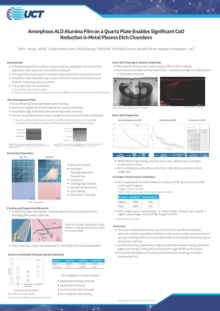
In order to address this problem, UCT and a chipmaking customer worked with coating partner Inficon to come up with a novel solution. This solution involved coating the quartz parts with a sacrificial atomic layer deposition (ALD) film and developing a cleaning and texturing refurbishment process.

ALD is used broadly within semiconductor devices, but ALD films are not used on the parts within production chambers. A high quality, conformal ALD film and a cleaning process with high selectivity to the quartz base material would be ideal to enable by-product removal. Texturing the surface would increase the mechanical adhesion of the by-product layer, reducing the risk of delamination. The highly conformal nature of the ALD film maintains the target surface texture and helps manage surface trace metals.

These quartz parts with a specified surface roughness were coated with at least 200nm of amorphous ALD Al2O3 films. After running in a chamber under process conditions, the by-product coated parts underwent a proprietary chemical strip process developed to remove the ALD Al2O3 film and by-product deposition. The quartz substrate showed no degradation as characterized using x-ray fluorescence (XRF), particle level, and roughness measurements.


This process is now qualified with the customer and the recycled quartz parts provide >75% reduction in Cost of Ownership (CoO). The ALD material was >99.999% pure, fully amorphous, and had a low intrinsic surface roughness. The delamination failure, which typically impacts 16% of all installed parts, was eliminated and a higher percentage overall of the quartz parts met mean time between clean (MTBC) target or full PM. The results were presented at the 2022 ALD/ALE conference with the above poster.

Monday, September 26, 2022

Wafer scale microwire (TMW) solar cell with 21.1% efficiency using NCD ALD tool (Lucida D200)

[PV Magazine] Korean scientists have built a wafer-scale radial junction solar cell with tapered microwires and a surface passivation layer made of aluminum oxide. The device showed the highest power conversion efficiency among the previously reported microwire solar cells.


Crystalline silicon TMW solar cells are considered a potential alternative to conventional solar cells as these devices require thinner silicon wafers instead of the industry standard 160 µm thick wafers. “This could reduce manufacturing capital expenditure by 48% and module cost by 28%,” the Korean group claims.


Crystalline silicon TMW solar cells are considered a potential alternative to conventional solar cells as they require thinner silicon wafers instead of the industry standard 160 µm thick wafers. Image: Kangwon National University


A 10 nm-thick Al2O3 passivation layer was deposited on the front side of the wafer using ALD (Lucida D200, NCD) as reported in the publication below.

Choi, D., Hwang, I., Lee, Y., Lee, M., Um, H. D., & Seo, K. (2022). Wafer‐Scale Radial Junction Solar Cells with 21.1% Efficiency Using c‐Si Microwires. Advanced Functional Materials, 2208377.

The new Girard Perregaux Tourbillon with Three Flying Bridges Bucherer BLUE coloured by Atomic Layer Deposition


Founded in 1888, Bucherer is one of the oldest houses specializing in watches and jewellery. One of the world’s largest retailers, it also brought several industry-leading initiatives like the way they handle CPO and the creation of Bucherer BLUE. The Bucherer BLUE concept was presented in 2016, it consists of gathering different brands under the same creative platform with a shared DNA, and the will to present innovative, creative collaborations. And today, in exclusivity, we're able to introduce to you the 3 latest creations forming the Bucherer BLUE Collection. Meet the new Girard Perregaux Tourbillon with Three Flying Bridges Bucherer BLUE, the H. Moser & Cie Streamliner Tourbillon Bucherer BLUE and the (very cool) L’Epée 1839 Time Fast Bucherer BLUE.
 

-----------------------------------------------


Meet Atlant3D Technologies with CEO Maksym Plakhotnyuk


ATLANT 3D Nanosystem is part of the SSAP Europe portfolio and is a global pioneer combining unique advanced technologies to enable atomic layer 3D printing. Listen to their CEO & Founder Maksym Plakhotnyuk as he gives us the rundown on his cutting-edge technology that has the potential to change the world in big ways. 🌎 Learn more: https://www.atlant3d.com/

Bottom-up PEALD of SiO2 by growth inhibition for seamless gap-fill process

Bottom-up plasma-enhanced atomic layer deposition of SiO2 by utilizing growth inhibition using NH3 plasma pre-treatment for seamless gap-fill process

Yoenju Choi, Taehoon Kim, Hangyul Lee, Jusung Park, Juhwan Park, Dongho Ryu & Woojin Jeon

Scientific Reports volume 12, Article number: 15756 (2022)

The design-rule shrinkage in semiconductor devices is a challenge at every step of the integration process. In the gap-fill process for isolation, the seam and void formation cannot be suppressed by using a deposition process, which even has excellent step coverage. To achieve seamless gap fill in the high-aspect-ratio structure, which has a non-ideal etch profile such as a negative slope, the deposition process should be able to realize the “bottom-up growth” behavior. In this work, the bottom-up growth of a SiO2 plasma-enhanced atomic layer deposition (PE-ALD) process in a trench structure was investigated by using a growth inhibition process employing plasma treatment. N2 and NH3 plasma pre-treatments were employed to suppress the growth of the SiO2 PE-ALD process without any contamination, and the inhibition mechanism was investigated by performing surface chemistry analyses using X-ray photoelectron spectroscopy. Furthermore, the gap-fill characteristics of the SiO2 PE-ALD process were examined, depending on the process conditions of NH3 plasma pre-treatment, by performing cross-sectional field emission scanning electron microscopy measurements. Finally, a seamless gap-fill process in a high-aspect-ratio trench pattern was achieved by the bottom-up growth behavior of SiO2 PE-ALD using NH3 plasma pre-treatment.


AlixLabs proudly announce its Advisory Board

AlixLabs from Lund, Sweden, has developed a new, innovative method for manufacturing semiconductor components with a high degree of packing, eliminating several steps in the semiconductor manufacturing process - Atomic Layer Etch Pitch Splitting (APS)*. The method makes the components cheaper and less resource-intensive to manufacture in high-volume semiconductor wafer fabrication and can open up a new path for a more sustainable mass production of electronic products. The method also makes it possible to manufacture tiny semiconductor components accurately and efficiently with more manageable wafer fab equipment investments.

The company is pleased to announce an Advisory Board with long-term semiconductor industry and business experts and academic leadership. In a statement from Dr. Jonas Sundqvist, CEO and co-founder of AlixLabs, he said, "Our Advisory Board adds a new level of engagement with the semiconductor industry and leading research centers needed to transfer the APS technology into high volume manufacturing. Besides strategic business decisions, we must build an ecosystem around our disruptive patterning technology. With their support, we will be able to deeply engage the semiconductor ecosystem on all levels and in all supply sectors, from materials and equipment suppliers to the wafer fabs and recognized R&D labs and institutes in this amazing industry".


Lita Shon-Roy – President/CEO and Founder of TECHCET—has worked throughout the semiconductor supply chain, leading strategy, business development, marketing, and sales for chip designers, equipment OEMs, and material suppliers for over 30 years. Her experience spans from process development of SRAMs to business development of gases & precursors. She developed new business opportunities for companies such as RASIRC/Matheson Gases, Air Products & Chemicals, and IPEC/Speedfam, and managed marketing and sales in companies such as Air Products/Schumacher, Brooktree/Rockwell, and Hughes Aircraft. Ms. Shon-Roy is considered one of the leading experts in electronic materials market analysis and business development. She has authored and co-authored 100’s of articles, reports, and texts on semiconductor process materials markets, trends, and worldwide supply chain issues. She holds an Masters Business Administration (MBA) from California State University, Dominguez Hills, a Master of Science (MS) in Electrical Engineering with a specialty in Solid State Physics from the University of Southern California, and a Bachelor of Science (BS) in Chemical Engineering from UC San Diego.

Prof. dr. Fred Roozeboom is emeritus/guest professor in the Inorganic Membranes group at the University of Twente and consultant to the high-tech industry. From 2007 until Dec. 2021 he was a part-time, full professor at TU Eindhoven in the group Plasma & Materials Processing, and from 2009-2021 he was Senior Technical Advisor at TNO Holst Centre, Eindhoven, aiming at new applications in Atomic Layer Deposition and Etching, area-selective ALD, Li-ion micro-batteries, and EUV optical lifetime. From Sept. 2021 - Sept. 2022 he was a Research Fellow at LionVolt, a start-up, working on pilot line production of 3D thin-film Li-batteries on metal foil. Fred is co-/author of >200 publications (h-index 42), 5 book chapters, 39 granted US patents, co-/editor of 51 conference proceedings on semiconductor & microsystems processing, and executive
editor of open access journal Atomic Layer Deposition. He was or is active in conference committees for the Materials Research Society, Electrochemical Society, American Vacuum Society, IEEE, DPS-Japan, and SEMI Europe Semiconductor Technology Programs Committee.

Dr Jacques Kools has over 35 years of experience in nanotechnology R&D, focusing on capital equipment and process for vacuum etch and deposition processes. He started his career at Philips Research, Eindhoven, The Netherlands, working on reactive ion beam and laser etch processes and magnetic materials. He worked in various roles in the semiconductor equipment industry in Silicon Valley, most recently as Vice President of Technology and Director of Strategic Marketing at Veeco Instruments (NASDAQ: VECO). His current position is CEO and founder of Encapsulix, a supplier of Atomic Layer Deposition ( ALD) equipment and process technology. Dr. Kools holds a Ph.D. from the Eindhoven University of Technology. He has published extensively with more than 100 refereed papers, including more than 10 invited reviews and more than 20 US patents (h index of 30 and i10 index of 60).

Atomic Layer Deposition (ALD) - Compound Semiconductor magazine interview with Beneq

Richard Stevenson, Editor of Compound Semiconductor magazine, talks to Mikko Söderlund, Beneq's Head of Sales for its Semiconductor ALD Business Unit, about the phenomenal interest in this sector.


Compound Semiconductor Magazine: www.compoundsemiconductor.net
Beneq's Semiconductor ALD Business: www.beneq.com/en/products/semiconductors


Thursday, September 22, 2022

Oxford Instruments and ITRI report GaN HEMT device performance by ALD and ALE

GaN HEMT device performance - Oxford Instruments and ITRI announce breakthrough development in GaN HEMT device performance


Oxford Instruments alongside its research partner Industrial Technology Research Institute (ITRI) can today share new and exciting technology developments that will significantly benefit key hyper-growth electric vehicle, datacentre and 5G markets. The technology developments allow critical transistor components to operate at higher voltages which increases performance and reliability, while also achieving a safer and more energy efficient (normally off ‘E-mode’) operation compared to existing devices. The new GaN (gallium nitride) HEMT device architecture is defined by a recessed and insulated gate junction into the AlGaN layer, and this device is referred to as GaN MISHEMT.

In September 2021, Oxford Instruments Plasma Technology and ITRI announced a cooperative research program for next-gen compound semiconductors. This latest breakthrough is an example of that collaboration delivering on its goal of accelerating technology to benefit the partners, their regions and wider global markets. Since that announcement, Oxford Instruments has also unveiled an exclusive supply deal with Laytec, who’s endpoint technology is used to control the GaN MISHEMT recess gate depth. Recess depth accuracy and repeatability is critical to tune the device performance characteristics, and LayTec’s technology is designed specifically for this application achieves target depth accuracy of ±0.5nm. ITRI provides pilot production and value-added services, including process verification and product development. ITRI’s integration services, especially this GaN development project, have proved incredibly beneficial, which quickly proved out the higher performance of GaN MISHEMT and provided a lower risk and faster route to market for the device.

Klaas Wisniewski, Oxford Instruments Strategic Business Development Director commented: “We have excellent strategic partners and customers like Enkris, ITRI, LayTec and ROHM, and our GaN solutions are positioned strongly to serve, grow and gain from big opportunity markets. Our leading Atomic Layer Etch (ALE) and Atomic Layer Deposition (ALD) technology is raising material engineering performance to achieve new levels of surface quality and defect reduction, to meet the growing demand for higher performing devices.” Klaas also added: “With our technology partner ITRI, high volume GaN manufacturing customers and our focussed investment into high value and proprietary process solutions, we expect the GaN device market to be a key driver for our business and technology roadmap.”

Klaas Wisniewski presented a talk entitled “Enhancing GaN HEMT Performance for Power Electronics Applications with Atomic Scale Processing Production Solutions” at Semicon Taiwan Sept 14-16, 2022, TaiNEX 1, Taipei, Taiwan. Please get in touch with us to discuss our latest data and opportunities for partnership and collaboration.

Monday, September 19, 2022

New 2022 Critical Materials Reports from TECHCET

New 2022 Critical Materials Reports from TECHCET LLC CA. TECHCET provides Business Intelligence and Analysis on the Electronics and Semiconductor Materials Markets through our annually published Critical Material ReportsTM (CMR). TECHCET CMR’s are developed through extensive market research led by industry specialists. Each CMR includes Quarterly Updates, emails on Analyst’s Alerts of breaking news, and a phone consultation with the analyst.


Sunday, September 18, 2022

Imec´s sustainable-semiconductor program is a success right away!

Imec´s sustainable-semiconductor program (LINK) seems to be a success right away:
  • Less than a year after its official launch, some of the leading consumer electronics and semiconductor manufacturing players have signed up as partners in imec’s program for Sustainable Semiconductor Technologies and Systems (SSTS).
  • Apple joined the program Apple joins Imec's new Sustainable Semiconductor research program | iMore
  • The program assesses the environmental impact of new technologies, identifies high-impact problems, and defines semiconductor manufacturing solutions with less environmental impact.
  • In this way, the program gathers the semiconductor value chain to jointly target net-zero emissions for chip manufacturing.
  • One good reason for success is most probably that Lars-Åke Ragnarsson from Sweden is the program director of sustainable semiconductor technologies and systems (SSTS) at imec.

More information:


Samsung to focus on treatment of gas used in chip production to achieve net-zero emissions

A major cause of greenhouse gas emissions is process gas used in semiconductor wafer manufacturing comes from processing equipment such as reactive ion etching (RIE) and deposition (CVD and ALD). You can read and watch an interview here and study that paper that was recently published by me and my professor friends Henrik Pedersen and Sean Barry:


Green CVD-Toward a sustainable philosophy for thin film deposition by chemical vapor deposition

It is almost obvious that higher VPs at Samsung and TSMC (LINK) did just that ;-)

[Korea Herald, Link below] Advancing abatement technologies to reduce carbon emissions is the top priority in the Samsung Electronics semiconductor unit's goal to become carbon neutral by 2050, a top official said Friday.

"Treatment of gas used to manufacture semiconductor chips is our biggest focus in our spending (to achieve net-zero emissions)," Song Doo-guen, executive vice president and head of the Environment & Safety Center at Samsung Electronics, told reporters at a briefing in Seoul.


According to the article, Song Doo-guen, executive vice president and head of the Environment & Safety Center at Samsung Electronics, speaks at a briefing in Seoul, Friday and announced that:
  • Samsung has pledged a 7 trillion won ($5 billion) investment to achieve its climate ambitions, and announced that it had recently joined RE100, a coalition comprising 380 global enterprises committed to becoming 100 percent renewable.
  • Alongside the plan to cut direct carbon emissions, Samsung has also laid out a raft of plans to reduce indirect emissions, mainly by pursuing ultralow-power chip products.
  • Other eco-conscious plans it has drawn up include capping the maximum use of freshwater to 300,000 tons a day by 2030 and eradicating gaseous and liquid pollutants by 2040 with treatment technology.
Source: Samsung chip plants look to stamp out carbon footprint (koreaherald.com)

Inside TSMC, the Taiwanese chipmaking giant that’s building a new plant in Phoenix

[CNBC, link below] Recently CNBC got an exclusive tour of the US$ 12 billion semiconductor fab, in Phoenix, Arizona, where TSMC will start making 5 nm chips in 2024. The company says it will ramp up to produce 20,000 wafers each month.

“This project is designed as a 5 nm fab. Actually, it’s a copy from the fab we have in Taiwan,” Chen said.

Nearby, one of the world’s largest cranes was lifted to its full height of 200 feet. The 2,300-ton crane was brought to the site on 153 semi trucks. Site supervisor Jim White said contractors have moved nearly 4 million cubic yards of dirt and have used more than 260 million gallons of water since construction began in April.


Building a fab and making chips takes an incredible amount of water, not an abundant resource in the middle of the desert. Arizona’s biggest water source is groundwater, but deep wells at big farms are using water up faster than it’s naturally replenished. Chen said TSMC needs around 4.7 million gallons of water each day to support production. In Arizona, TSMC said, an on-site water treatment center will recycle up to 90% of water used at the fab.

Full article with video:

Friday, September 16, 2022

The fast-growing technology start-up Chipmetrics moved to Photonics Center

(Original Article: LINK) In August, Photonics Center received a new business resident as Chipmetrics Oy moved to the centre's premises. Founded in 2019, the company has started its business rapidly: last year's turnover was already over EUR 700,000.

Chipmetrics’ CEO Mikko Utriainen is looking forward to testing Photonics Center’s potential as a research and development environment. The centre offers a range of equipment that is ideal for Chipmetrics’ needs, such as an ALD reactor, which can be used to test the functionality of products.

“It is also an enormous help to have the personnel of the University of Eastern Finland available for support at an hourly rate. Photonics Center’s equipment is demanding and requires highly skilled professionals. As a whole, the greatest benefit is certainly that all these resources are available in one place. No facilities of the same standard can be found in Eastern Finland; in fact, the only option in Finland would have been to transfer the company’s operations to Helsinki.”


Of the individual Photonics Center resources, the most important attraction factor for Chipmetrics was cleanrooms.

“The handling and development of our products must all be done in cleanrooms, as is typical in the semiconductor industry. That is why they are a necessity for a company like us.”

Measurement solution to increase efficiency in processes worth billions

Chipmetrics specialises in ALD technology. ALD stands for atomic layer deposition, which enablesmeans coating three-dimensional objects with thin film structures. ALD is a growing sector: according to Utriainen, the global market is approaching EUR 3 billion.

“ALD is used, for example, in semiconductor components, batteries and optical filters with 3D structures that are difficult to implement and coat. A smooth uniform thin film coating is very difficult, but it is even more difficult to measure whether the coating is really uniform smooth.”

Chipmetrics’ PillarHall solution is capable of very accurate measurement, enabling semiconductor manufacturers to enhance their own processes. Even small improvements can be valuable.

“The investments made by giant electronics companies are often in billions. A manufacturer of semiconductor equipment, which is best able to demonstrate its technical performance, can win a significantly sizeable deal in a big chip manufacturer’s factory investment. It is often important for our customer companies to be able to demonstrate to their own customers how well they can achieve a functioning process,” Utriainen explains.

Investors getting interested

Chipmetrics is a spinoff company that originated from a VTT research project. Utriainen was involved in the development of technology already at VTT. The company was established in 2019 and operational activities began at the end of 2020 when IPR rights were transferred to Chipmetrics.

The first full financial year was already good for the company: turnover was EUR 703,000 and profit was EUR 84,000. Chipmetrics just recently finished its start-upseed funding round, which netted EUR 340,000 for the company. The round was led by the North Karelia Growth Fund and four private investors. With the help of new funding, CEO Utriainen plans to develop the company’s product portfolio and expand the international sales network.

“ALD technology is complex, and it has been one of the key challenges for investors: sponsors naturally want to understand what they are participating in. We have now got investors involved in Finland, which also increases interest abroad.”

“It is our pleasure to welcome Chipmetrics to Photonics Center,” says Pauliina Pikkujämsä, Director of Business Services at Business Joensuu. “Photonics is one of the top industries in Joensuu, and Photonics Center is a direct investment in the operations of companies that manufacture or utilise photonics. ALD technology, the field of Chipmetrics, also has huge growth potential internationally. We’d like to have more such growth companies in the Joensuu region.”

Further information:

Pauliina Pikkujämsä

Business Services Director, Invest In and Relocation Services, pauliina.pikkujamsa@businessjoensuu.fi, +358 40,743 4362

Mikko Utriainen

Chipmetrics Oy, CEO, mikko.utriainen@chipmetrics.com, +358 40,753 7415


Business Joensuu

Business Joensuu Oy offers services for launching companies, growth and internationalisation, investing and setting up operations in an area, and space and event services of the Joensuu Science Park. Business Joensuu also produces growth and competitiveness programmes which create the best conditions for companies to operate in the Joensuu area.

Chipmetrics

Chipmetrics Oy is an ALD (Atomic Layer Deposition) technology company. Chipmetrics is the market leader in delivering productised nanotechnological high aspect ratio test structures to the semiconductor industry and emerging ALD applications. Chipmetrics’ headquarters are located in Joensuu. Further information: www.chipmetrics.com

Picture credits: Chipmetrics Oy

Thursday, September 15, 2022

ATLANT 3D Nanosystems Secures 15M USD Investments to Enable Atomic Layer Advanced Manufacturing for Electronics

Copenhagen September 12, 2022: ATLANT 3D Nanosystems (ATLANT 3D), today announced the closure of their capital raise of 15M USD. The round was led by UK venture capital firm West HillCapital and further supported by existing investors including a leading Japanese corporation. The funding is the largest joint Series A round in Denmark outside of life sciences and software.

The funding will be used to get one step closer to ATLANT 3D’s vision to create a network-centric smart advanced manufacturing infrastructure based on its proprietary technology and know-how and integrate it in the future with other advanced technologies. ATLANT 3D aims to develop a network of advanced manufacturing hubs – the A-hubs – across the globe to enable a radical innovation ecosystem for next-generation micro and nanoelectronics prototyping and manufacturing.

ATLANT 3D is the first and only company to crack the code for a radically new way of doing micro and nano processing. ATLANT 3D’sNanofabricator™ enables advanced manufacturing with AI solutions which allows direct patterning on complex surfaces, various substrate materials, plain wafers, and textures with existing structures or devices. ATLANT 3D technology has a unique configuration that allows atomically precise processing at micro and zero gravity. In general, it decreases the time and cost of processing from years and months to days, and gives unprecedented flexibility for material innovation, prototyping, and production of micro and nanodevices, replacing the previous cleanroom-based complex process flows.


“The existing process-intensive manufacturing method is a limiting factor in the future of electronics development. Due to its inflexibility, the current multi-step process is at the root of our current global supply chain crises, causing a shortage of electronics devices and bringing high barriers to innovation. “, says Dr. Maksym Plakhotnyuk, CEO and Founder of ATLANT 3D. “At ATLANT 3D, we have invented a unique technological platform that enables what was previously impossible. Imagine that new advanced materials, devices, and applications that you use today for your smart life or for the industry can be manufactured in-house, with flexibility, and sustainability in mind. The process can be fully digital, cost-effective, and provide a possibility for rapid innovation with atomic precision. The recently raised funding will enable us to continue the fast technology and product development and expand ATLANT 3D to the first international market.”

” We see a huge potential in ATLANT 3Ds' groundbreaking technology. We were impressed by the company’s grand vision and the way how ATLANT 3D technology is ready to disrupttodisrupt the conventional microfabrication approach” says Alan Richards, Partner, and Co-Founder of West Hill Capital.


ATLANT 3D is a Danish deep-tech company founded in 2018 developing a fundamentally different and innovative micro and nanofabrication platform technology that enables atomically precise advanced manufacturing of advanced materials and electronics with the vision to revolutionize electronics atom by atom. Since 2020ATLANT 3D secured a number of customers, leading global industrial companies and organizations, in space, semiconductor, and electronics industries.


Since 2014, West Hill Capital has arranged investment of $500 million into 40 early-stage high-growth companies in the UK and Denmark. In 2021, West Hill’sportfolio company Humio was acquired by USA Nasdaq-listed Crowdstrike Holdings for US$400 million, one of the largest Danish private company exits that year.b

AlixLabs AB today announced that the company has been granted a second patent in the USA relating to Atomic Layer Etch Pitch Splitting (APS) for semiconductor manufacturing

MON, SEP 12, 2022 21:19 CET. AlixLabs from Lund, Sweden, has developed a new, innovative method for manufacturing semiconductor components with a high degree of packing, eliminating several steps in the semiconductor manufacturing process - Atomic Layer Etch Pitch Splitting (APS)*. The method makes the components cheaper and less resource-intensive to manufacture and can open up a new path for a more sustainable mass production of electronic products. The method also makes it possible to manufacture tiny semiconductor components accurately and efficiently with manageable wafer fab equipment investments.

The company is now pleased to announce having been granted a second patent in the USA. USA is one of the most important markets for leading-edge semiconductor manufacturing, a huge industrial and consumer market for the most advanced electronic products and hence crucial for AlixLabs to protect its innovative APS process by IP.

In a statement from Dr. Dmitry Suyatin, CTO and co-founder of AlixLabs on the origin of the invention and R&D activities in Lund, he said "Our key technology is based on a surprising discovery that sidewalls act as a topographical mask in Atomic Layer Etch Processes. This technology has been proven for such different materials as Gallium Phosphide (GaP), Silicon (Si) and Tantalum Nitride (TaN) – all being critical materials to the semiconductor and optoelectronic industry. Besides already having secured a granted the first US and Taiwan patent, we are now delighted to announce that our second US patent has also been granted and that we have more patent applications in the pipeline".


AlixLabs: Amin Karimi, Reza Jafari Jam, Yoana Ilarionova, Jonas Sundqvist and Dmitry Suyatin.

Dr. Amin Karimi, R&D and Operation Manager, added, "I am delighted to add that ALixLabs has been finalized a 1 Million SEK Vinnova funded project to verify the APS technology in the fabrication and electrical characterization of nanowire test transistor architectures this summer". Dr. Jonas Sundqvist, CEO and co-founder of AlixLabs, concluded that "The strategy as we advance is to successfully transfer the APS technology to 300 mm wafer processing and making it readily available for process demonstration for the leading IDMs & Foundries. We don't only hope to cut cost in semiconductor manufacturing but also to reduce the energy and clean water demand and output of greenhouse gasses during chip manufacturing considerably. This is not by itself a Green Fab Technology. However, it takes one small step in the right direction."

* Atomic Layer Etch Pitch Splitting (APS). As previously reported (April 30, 2021), The US Patent Office has approved AlixLabs's patent application for nanofabrication by ALE Pitch Splitting (APS). The US Patent Office has issued a patent (US10930515) on February 23, 2021 and now the second patnet (US11424130) on August 23, 2022. The patents covers methods to split nanostructures in half by a single process step using Atomic Layer Etching (ALE). The method can have a significant impact on the semiconductor industry by enabling sustainable scaling of electronic components and shrink chip designs further in a cost-effective way. The method is complementary for single exposure Immersion and Extreme UV (EUV) Lithography and corresponding multiple patterning technologies like self-aligned double and quadruple patterning (SADP resp. SAQP) as well as multiple exposure lithography-etch and directed self-assembly (DSA).

Jonas Sundqvist, CEO of AlixLabs, phone +46 767 63 94 67, email jonas@alixlabs.com.

AlixLabs (www.alixlab.com) is an innovative startup founded in 2019 in Lund, Sweden, enabling the semiconductor industry to scale down Logic and Memory components in a cost-effective manner by the use of ALE Pitch Splitting (APS).

TSMC to double energy efficiency and clean water consumption for semiconductor wafer manufacturing

According to TSMC 2021 Sustainability Report, they aim to by 2030, amongst many goals & actions:

  • double energy efficiency after five years of mass production for each process technology
  • reduce unit water consumption (liter/12-inch equivalent wafer mask layers) by 30% (Base year: 2010)
Link to report: e-all.pdf (tsmc.com)


Friday, September 9, 2022

Semiconductor Equipment Consumables - Silicon Parts, in High Demand with Continued Shift Toward Asia

San Diego, CA, September 8, 2022: TECHCET—the electronic materials advisory firm providing business and technology information— reports that the demand for high-purity Silicon Parts for semiconductor manufacturing equipment will continue strong in 2022. This forecast is expected as equipment sales grow and fabs expansions continue to ramp. The Silicon Parts market is expected to top US $900 million, a 10% increase from US $824 million in 2021. TECHCET forecasts the 2021 to 2026 CAGR for this market to grow at an almost 6% rate, as shown in the graph below and described further in TECHCET’s Newly Released Critical Materials Report™ (CMR) on Silicon Equipment Components.


“Silicon Parts are primarily consumed in etch equipment systems, so market growth is heavily tied to chip production and influenced by new etch equipment sales,” states Dan Tracy, senior analyst at TECHCET. Additionally, the replacement part segment represents about 70% of the market as these consumable parts have a finite lifetime, and need to be replaced per a fab’s maintenance schedule. Given industry fab investment trends, about 66% of the new and replacement parts are for the 300 mm fab manufacturing segment.

To read the full article, go to: https://lnkd.in/gK-fp8H9

For more information details on the Silicon Parts market and growth trajectory, go to: https://lnkd.in/gM9GMNUs

SEMICON Europa 15 to 18 November, Munich Germany - Chips Powering the Data Age

SEMICON Europa, co-located with electronica, returns to Messe München 15-18 November, Munich, Germany with an exhibition, conferences, forums, technical sessions and business networking to help you expand your business.

Themed Chips Powering the Data Age, SEMICON Europa 2022 will convene technology experts and visionaries for insights into the latest technology, materials, and process innovations powering digital transformation and the next wave of semiconductor industry growth.

As usual there will be a Materials Innovation session. This session will explore materials innovation developments and challenges related to atomic-scale processing and control of interfaces, morphology, composition, and 3D conformality for these applications.

This time with an extra touch by me, Jonas Sundqvist, and Lita Shon-Roy, President of TECHCET LLC CA and the team from San Diego and the Critical Materials Council comes to Europe - surfs up stay tuned for more information!

Europe Chemical Supply Chain – Impact of Fab Expansions

Risk of Supply Interruption Grows With an Increase in Imports

San Diego, CA, May 17, 2022: TECHCET—the electronic materials advisory firm providing business and technology information— examined critical materials dependencies of Europe’s expanding chip-making industry. Six high purity chemicals were identified as having the highest risk of supply interruption by major Europe chip fabricators: liquid and gas hydrochloric acid (HCl), sulfuric acid (H2SO4), hydrofluoric acid (HF), ammonia hydroxide (NH4OH), and isopropyl alcohol (IPA). Demand for these materials is expected to grow 40+% over the next 5 years, as shown in TECHCET’s study titled “The Impact Of Chip Expansions On The Europe Wet Chemical Supply Chain Report.” By 2027, more than 50% of total demand will have to be supplied by imports should there be no additional expansion in local chemical production.


Monday, September 5, 2022

Chipmetrics announces completion of the seed investment round

Joensuu, Pohjois-Karjala Sep 4, 2022 (Issuewire.com) - Chipmetrics Ltd, the ALD (Atomic Layer Deposition) technology company and the market leader of productized 3D ultra-high aspect ratio test elements for semiconductor and advanced material manufacturing announced it has closed its 340.000 euro seed round. The investment round was led by Redstone through its North Karelia Growth Fund, alongside four private semiconductor and ALD experts.


“Our mission is to support our customers in the development of Atomic Layer Processes and their 3D applications by offering innovative, fast, and accurate measurement solutions. With this seed funding, we will develop our product portfolio and measurement concept offering and expand our global sales network.” Says Mikko Utriainen, Founder & CEO of Chipmetrics.

“I invested in Chipmetrics since I know the ALD market very well and Chipmetrics has clear potential to grow with the increasing adoption of ALD in the semiconductor industry,” says Jonas Sundqvist, a respected ALD consultant and entrepreneur from Dresden, Germany.

Other private investors, Matias Koski and James Song will support the company with their industry networks. Mr. Song will support building distribution in South Korea and beyond. Mr. Koski is based in Hong Kong, with a background in mobile phones and augmented reality.

Private investors also include Kai Seikku, a respected leader in the semiconductor industry, presently President and CEO of Okmetic and Vice General Manager & EVP of NSIG group.

Kaj Hagros, managing partner for Redstone Nordics and general partner for North Karelia Growth Fund comments: “Redstone’s existing collaborations with investors and corporations globally open opportunities for partnerships and business development. Chipmetrics has extraordinarily solid technology and a good market position, fully functional products already shipping, a great team, and clear plans to execute growth. Delighted to lead the round”.

Chipmetrics’ conformality measurement method based on PillarHall® Lateral High Aspect Ratio (LHAR) test chips has already gained a solid position in conformality measurements among ALD/CVD/BCD thin film process developers. The customers are leading semiconductor industry equipment suppliers and equipment users. The advantages of PillarHall® LHAR technology are a unique and convenient user interface, high accuracy and speed, and cost-effectiveness in challenging 3D measurements.

About Chipmetrics

Chipmetrics Ltd is an ALD (Atomic Layer Deposition) technology company founded in 2019. Chipmetrics is the market leader as a supplier of productized nanotechnological high aspect ratio test structures for the semiconductor industry and ALD applications. Chipmetrics' head office is in Joensuu, Finland, and it has sales representatives in Japan, South Korea, Taiwan, Singapore, China, and Germany. More information: www.chipmetrics.com

Mikko Utriainen, CEO, Chipmetrics Ltd

Email: mikko.utriainen@chipmetrics.com; tel. +358407537415

About Redstone

Redstone is a Berlin-based venture capital firm managing 10 sector funds with 360 closed transactions. Redstone is the general partner for North Karelia Growth Fund, investing in recently established and young companies from the region, particularly in the sectors of digitalization, forest and bio-economy, photonics, travel and creative industries, and material sciences. More information: www.redstone.vc

Kaj Hagros, Managing Partner, Redstone Nordics

Sunday, September 4, 2022

3D Printing by ALD with Atlant 3D's Maksym Plakhotnyuk - ALD Stories

Episode 16 features Dr. Maksym Plakhotnyuk, the CEO and Founder of Atlant 3D Nanosystems. Atlant 3D produces the world's first reactor for direct writing of ALD - the ultimate area-selective ALD process. Their Nanofabricator tool will could be the enabling technology for on-demand printing of microelectronics. In this episode, Maksym tells Tyler about the company's origins, their deal with NASA to create a 0G ALD reactor and Maksym's own history as an entrepreneur. 

In this episode: 00:00 Introduction 01:53 Maksym's Background & Atlant 3D Roots 19:03 Atlant 3D Name Origins 22:00 Atlant 3D Microreactor 36:28 NASA Deal and 0G Reactor 

Follow Maksym and Atlant 3D on Twitter: @MPlakhotnyuk & @Atlant3d 

Check out the technology at www.atlant3d.com

Tokyo Electron is forcastiong high continued sales in semiconductor equipment sales 2023 - slow down in DRAM

Tokyo electron forecast for FY2023 SPE Division New Equipment Sales Forecast - DRAM is retracting in 2023 but you can´t say that about Logic and Non-Volatile Memory (3DNAND Flash). Full power ahead for ALD and its friends!


One good freind of ALD is Etch. Tokyo Electron is spending quite some development Yen Billions by building a new facility just for etch development.


Samsung Electronics Breaks Ground on New Semiconductor R&D Complex in Giheung, Korea

Samsung to invest KRW 20 trillion by 2028 to build advanced research facility

Samsung Electronics recently broke ground for a new semiconductor research and development complex in Giheung, Korea, aiming to extend its leadership in state-of-the-art semiconductor technology.

  • Samsung Electronics plans to invest about KRW 20 trillion by 2028 for the complex in an area covering about 109,000 square meters within its Giheung campus. 
  • The new facility will lead advanced research on next-generation devices and processes for memory and system semiconductors, as well as development of innovative new technologies based on a long-term roadmap.


Today’s groundbreaking ceremony was attended by Samsung Electronics Vice Chairman Jay Y. Lee, President and CEO Kye Hyun Kyung, President of the Memory Business Jung-Bae Lee, President of the Foundry Business Siyoung Choi and President of the S.LSI Business Yong-In Park, along with more than 100 employees.

“Our new state-of-the-art R&D complex will become a hub for innovation where the best research talent from around the world can come and grow together,” said President Kye Hyun Kyung, who also heads the Device Solutions (DS) Division. “We expect this new beginning will lay the foundation for sustainable growth of our semiconductor business.”


Samsung Electronics’ Giheung campus, located south of Seoul near the DS Division’s Hwaseong campus, is the birthplace of the world’s first 64Mb DRAM in 1992, marking the beginning of the company’s semiconductor leadership.

Resolving the Heat of Trimethylaluminum and Water Atomic Layer Deposition Half-Reactions

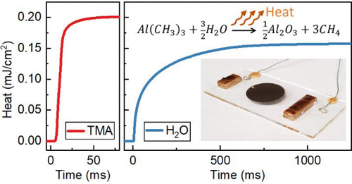
Here is a new way that I have not seen before how to monitor the half-reactions in ALD by using The pyroelectric thin-film calorimeter. It offers submillisecond temporal resolution and resolves precursor delivery and reaction kinetics. Thank you, Riikka, for sharing on Twitter.
 
Resolving the Heat of Trimethylaluminum and Water Atomic Layer Deposition Half-Reactions
Ashley R. Bielinski, Ethan P. Kamphaus, Lei Cheng, and Alex B.F. Martinson*
J. Am. Chem. Soc. 2022, 144, 33, 15203–15210
Publication Date:August 9, 2022
https://doi.org/10.1021/jacs.2c05460

Atomic layer deposition (ALD) is a surface synthesis technique that is characterized by self-limiting reactions between gas-phase precursors and a solid substrate. Although ALD processes have been demonstrated that span the periodic table, a greater understanding of the surface chemistry that affords ALD is necessary to enable greater precision, including area- and site-selective growth. We offer new insight into the thermodynamics and kinetics of the trimethylaluminum (TMA) and H2O ALD half-reactions with calibrated and time-resolved in situ pyroelectric calorimetry. The half-reactions produce 3.46 and 2.76 eV/Al heat, respectively, which is greater than the heat predicted by computational models based on crystalline Al2O3 substrates and closely aligned with the heat predicted by standard heats of formation. The pyroelectric thin-film calorimeter offers submillisecond temporal resolution that uniquely and clearly resolves precursor delivery and reaction kinetics. Both half-reactions are observed to exhibit multiple kinetic rates, with average TMA half-reaction rates at least 2 orders of magnitude faster than the H2O half-reaction kinetics. Comparing the experimental heat with published computational literature and additional first-principles modeling highlights the need to refine our models and mechanistic understanding of even the most ubiquitous ALD reactions.


Saturday, September 3, 2022

ASM reports that the ALD market is expected to grow by a CAGR of 16%-20% from 2020 to 2025

ASM International presented its Q2/2022 report in July and a new record orders of EUR 943 million driven by robust new node spending in logic/foundry and by recent wins in memory, particularly for ALD gap-fill in 3D-NAND and continued adoption of HKMG in DRAM.


ASM focuses on the single wafer market so the numbers presented does typically not include ALD Large Batch, which is dominated by Tokyo Electron and Kokusai. Back in 1999, ASM acquired Finnish legendary ALD company Microchemistry and its Pulsar 2000 cross-flow chamber ALD technology, which later took the market as the 300 mm version Pulsar 3000 for HfO2 in HKMG at Intel, TSMC, Samsung Globalfoundries, and others. Now it is interesting to follow how the success story continues also for DRAM HKMG. Since then, ASM has added PEALD from Genitech (South Korea) and Large Batch ALD (A412), and many other ALD process technologies. See recent announcements 2022 here:


So it is interesting that ASM has launched a new ALD Batch platform based on the now rather old A412 and the new TENZA to capture growth in Gap-fill - a stronghold for Lam Research.

The ALD market is driven by increased wafer starts in 300 mm for sub 45 nm nodes, 3DNAND and DRAM, and the ongoing fab expansions world-wide.


  • TechInsights expects WFE to increase by 21% in 2022 (July 2022)
  • Strongest growth in leading-edge nodes, spending on 7nm and below expected to grow from ~25% of WFE in 2020 to ~42% of WFE in 2025
  • Gartner expects total WFE to increase by 19% in 2022 (July 2022)
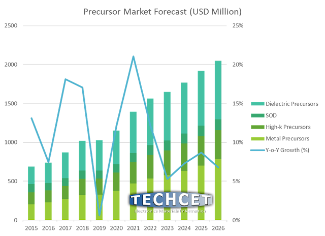
You can compare the TECHCET forecast on precursors where you can see high y-o-y growth going through 2021 and 2023 driven by increased 300 mm wafer production and a slowdown in 2023. Please find deeper dives, assessments and all the data in the TECHCET CMR reports: ALD / CVD Precursors (2) Archives - TECHCET CA LLC


Precursor market forecast 2022-2026 - Invited talk for TECHCET LLC CA in: AA2-TuM2-1 High ALD Equipment and Precursor Demand and 5-Year Forecast Due to Continued Semiconductor Device Scaling and Fab Expansions by Jonas Sundqvist.


Friday, September 2, 2022

Oxford Instruments validates Plasma Etch process as alternative to SiC CMP

Following Oxford Instruments announcement of its plasma alternative to CMP product, being launched at the International Conference on SiC and Related Materials (ICSCRM / ECSCRM) in Davos Switzerland on 11-16 September 2022, the company is sharing further news.


Oxford Instruments' non-contact plasma etch method of preparing SiC substrates for epitaxy delivers comparable results to CMP but with lower OPEX, higher device yield and a process window capable of supporting the transition to thinner wafers and therefore increasing wafers per boule.

In a feasibility project, carried out at a tier 1 SiC semiconductor manufacturing fab using whole wafers, the company found that performance of the new plasma substrate preparation technique is already equivalent to CMP for epitaxy readiness.

"This validation outcome is a significant milestone in our goal of creating a more cost-effective and sustainable technique for preparing SiC substrates for epitaxy" comments Klaas Wisniewski, Plasma Technology's strategic business development director, who also added: "Our Plasma epi-prep technology is hugely promising and currently compares favourably to existing alternatives, but has the potential to exponentially increase substrate production and meet the growing demand for SiC substrates in high growth markets."

Oxford Instruments will formally launch the plasma epi-prep solution at the ICSCRM, in Davos Switzerland 11-16 September 2022. In the conference technical sessions, the company will present their latest whole wafer epi and device results utilising its patented dry etch process.

There will also be an opportunity to speak in person at the event to discuss implementing plasma epi-prep in high volume manufacturing fabs.


Thursday, September 1, 2022

UPDATE - ASD 2023 will be held in Incheon National University South Korea April 2-5, 2023

ASD2023 will be held in Incheon National University from April 2nd to 5th, 2023. An official website will be online soon! Stay tuned!

Included is a session on ALD for Semiconductor applications.

UPDATE - website is online: http://asd2023.com


PROGRAM COMMITTEE:
  • Rudy J Wojtecki (IBM)
  • Stacey F Bent (Stanford University)
  • Annelies Delabie (imec)
  • John G Ekerdt (University of Texase)
  • Dennis Hausmann (Lam Research)
  • Erwin Kessels (Eindhoven University of Technology)
  • Adrie Mackus (Eindhoven University of Technology)
  • Ravi Kanjolia (EMD Electronics)
  • Gregory Parsons (North Carolina State University)
  • Robert Clark (TEL)
  • Sean Barry (Carleton University)
  • Han-Bo-Ram Lee (Incheon National University)
  • Marko Tuominen (ASM)
  • Sudipto Naskar (Intel)
  • Anuja DaSilva (Lam Research)
  • Kristen Colwell (Intel)

WEBINAR - Production-suitable 200 mm batch ALD/MLD thin film encapsulation toward flexible OLED manufacturing

New Picosun webinar available! Spend insightful 20 minutes watching our latest webinar "Production-suitable 200 mm batch ALD/MLD thin film encapsulation toward flexible OLED manufacturing" 


In this webinar, we present characterization and scale up results of a thin film encapsulation solution, demonstrated by scaling a previously small scale process into a production-proven 200 mm batch ALD system.


Supply Tightening Expected for Specialty Electronic Gases

Demand to outpace supply for NF3 and WF6 unless alternatives come into play

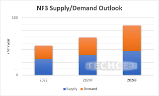
San Diego, CA, August 31, 2022: TECHCET—the electronic materials advisory firm providing business and technology information— reports that the supply of Specialty Gases, nitrogen trifluoride (NF3) and tungsten hexafluoride (WF6) for electronics could tighten amongst high projected demand by 2025-2026. This forecasted steep trajectory will challenge supply-chains to keep pace. However, alternatives being developed could interrupt this trend. Both NF3 and WF6 are part of a larger US$5 billion specialty gas segment forecasted to grow 30% over the next 5 years, to total US$6.5 billion by 2026. As shown below, NF3 is expected to grow even more steeply, 72% over the forecast period (as highlighted in TECHCET’s 2022 Critical Materials Report™ on Electronic Gases).


Alternatives for these gases are currently in development which could cause a shift in growth trends. The increasing demand for NF3 in electronic manufacturing, including flat-panel displays, has triggered concern among atmospheric scientists over emissions of nitrogen trifluoride, a potent greenhouse gas. Particularly, NF3 gas has a high Global Warming Potential (GWP) compared to other gases. Consequently, the electronics industry is looking at and considering processes for on-site fluorine generation that can use F2, in place of NF3, for chamber cleaning.

...

To read the full article, click here: https://lnkd.in/g25Fa3f2

For more information on the electronic gases market outlook, check out our newest Gases Critical Materials Report™ here: https://lnkd.in/gb95EBC

Wednesday, August 31, 2022

Webinar Atonarp’s Aston in-situ metrology solution for Spatial ALD


Register
Can’t attend the live webcast?  Register and we will send you a link to watch the recording at your convenience.

Overview:
 
Spatial ALD is emerging as a critical technology for the deposition of thin films for advanced memory and logic selective processing found in gate-all-around FETs, high aspect ratio contacts, DRAM capacitors, advanced NVM technology, and even self-aligned double patterning (SADP) lithography.  It has the promise of high throughput, highly conformal thin films using low temperature and low or no vacuum processing chambers.  However spatial ALD has challenges, gas mixing, platform rotation speed optimization, optimized gas purge flow, the variable concentration of reactant gases and safety considerations are some of the issues process engineers are working to optimize.  Atonarp’s Aston in-situ metrology solution will be reviewed and its key differentiations, being used by several spatial ALD OEMs to address these challenges, will be discussed.

What you’ll learn:
  • Spatial ALD advantages and challenges
     
  • Why speed with sensitivity and robustness matter in Spatial ALD metrology solutions
     
  • Aston Impact and Plasma metrology solutions and differentiation that is leading them to be used as key in-situ process control metrology in spatial ALD applications