Thursday, September 15, 2022

AlixLabs AB today announced that the company has been granted a second patent in the USA relating to Atomic Layer Etch Pitch Splitting (APS) for semiconductor manufacturing

MON, SEP 12, 2022 21:19 CET. AlixLabs from Lund, Sweden, has developed a new, innovative method for manufacturing semiconductor components with a high degree of packing, eliminating several steps in the semiconductor manufacturing process - Atomic Layer Etch Pitch Splitting (APS)*. The method makes the components cheaper and less resource-intensive to manufacture and can open up a new path for a more sustainable mass production of electronic products. The method also makes it possible to manufacture tiny semiconductor components accurately and efficiently with manageable wafer fab equipment investments.

The company is now pleased to announce having been granted a second patent in the USA. USA is one of the most important markets for leading-edge semiconductor manufacturing, a huge industrial and consumer market for the most advanced electronic products and hence crucial for AlixLabs to protect its innovative APS process by IP.

In a statement from Dr. Dmitry Suyatin, CTO and co-founder of AlixLabs on the origin of the invention and R&D activities in Lund, he said "Our key technology is based on a surprising discovery that sidewalls act as a topographical mask in Atomic Layer Etch Processes. This technology has been proven for such different materials as Gallium Phosphide (GaP), Silicon (Si) and Tantalum Nitride (TaN) – all being critical materials to the semiconductor and optoelectronic industry. Besides already having secured a granted the first US and Taiwan patent, we are now delighted to announce that our second US patent has also been granted and that we have more patent applications in the pipeline".


AlixLabs: Amin Karimi, Reza Jafari Jam, Yoana Ilarionova, Jonas Sundqvist and Dmitry Suyatin.

Dr. Amin Karimi, R&D and Operation Manager, added, "I am delighted to add that ALixLabs has been finalized a 1 Million SEK Vinnova funded project to verify the APS technology in the fabrication and electrical characterization of nanowire test transistor architectures this summer". Dr. Jonas Sundqvist, CEO and co-founder of AlixLabs, concluded that "The strategy as we advance is to successfully transfer the APS technology to 300 mm wafer processing and making it readily available for process demonstration for the leading IDMs & Foundries. We don't only hope to cut cost in semiconductor manufacturing but also to reduce the energy and clean water demand and output of greenhouse gasses during chip manufacturing considerably. This is not by itself a Green Fab Technology. However, it takes one small step in the right direction."

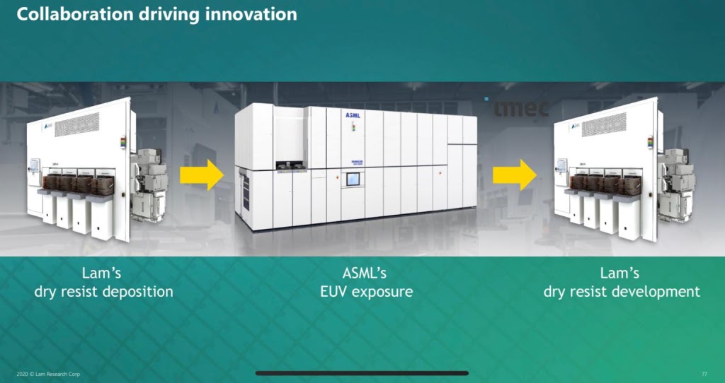
* Atomic Layer Etch Pitch Splitting (APS). As previously reported (April 30, 2021), The US Patent Office has approved AlixLabs's patent application for nanofabrication by ALE Pitch Splitting (APS). The US Patent Office has issued a patent (US10930515) on February 23, 2021 and now the second patnet (US11424130) on August 23, 2022. The patents covers methods to split nanostructures in half by a single process step using Atomic Layer Etching (ALE). The method can have a significant impact on the semiconductor industry by enabling sustainable scaling of electronic components and shrink chip designs further in a cost-effective way. The method is complementary for single exposure Immersion and Extreme UV (EUV) Lithography and corresponding multiple patterning technologies like self-aligned double and quadruple patterning (SADP resp. SAQP) as well as multiple exposure lithography-etch and directed self-assembly (DSA).

Jonas Sundqvist, CEO of AlixLabs, phone +46 767 63 94 67, email jonas@alixlabs.com.

AlixLabs (www.alixlab.com) is an innovative startup founded in 2019 in Lund, Sweden, enabling the semiconductor industry to scale down Logic and Memory components in a cost-effective manner by the use of ALE Pitch Splitting (APS).

TSMC to double energy efficiency and clean water consumption for semiconductor wafer manufacturing

According to TSMC 2021 Sustainability Report, they aim to by 2030, amongst many goals & actions:

  • double energy efficiency after five years of mass production for each process technology
  • reduce unit water consumption (liter/12-inch equivalent wafer mask layers) by 30% (Base year: 2010)
Link to report: e-all.pdf (tsmc.com)


Friday, September 9, 2022

Semiconductor Equipment Consumables - Silicon Parts, in High Demand with Continued Shift Toward Asia

San Diego, CA, September 8, 2022: TECHCET—the electronic materials advisory firm providing business and technology information— reports that the demand for high-purity Silicon Parts for semiconductor manufacturing equipment will continue strong in 2022. This forecast is expected as equipment sales grow and fabs expansions continue to ramp. The Silicon Parts market is expected to top US $900 million, a 10% increase from US $824 million in 2021. TECHCET forecasts the 2021 to 2026 CAGR for this market to grow at an almost 6% rate, as shown in the graph below and described further in TECHCET’s Newly Released Critical Materials Report™ (CMR) on Silicon Equipment Components.


“Silicon Parts are primarily consumed in etch equipment systems, so market growth is heavily tied to chip production and influenced by new etch equipment sales,” states Dan Tracy, senior analyst at TECHCET. Additionally, the replacement part segment represents about 70% of the market as these consumable parts have a finite lifetime, and need to be replaced per a fab’s maintenance schedule. Given industry fab investment trends, about 66% of the new and replacement parts are for the 300 mm fab manufacturing segment.

To read the full article, go to: https://lnkd.in/gK-fp8H9

For more information details on the Silicon Parts market and growth trajectory, go to: https://lnkd.in/gM9GMNUs

SEMICON Europa 15 to 18 November, Munich Germany - Chips Powering the Data Age

SEMICON Europa, co-located with electronica, returns to Messe München 15-18 November, Munich, Germany with an exhibition, conferences, forums, technical sessions and business networking to help you expand your business.

Themed Chips Powering the Data Age, SEMICON Europa 2022 will convene technology experts and visionaries for insights into the latest technology, materials, and process innovations powering digital transformation and the next wave of semiconductor industry growth.

As usual there will be a Materials Innovation session. This session will explore materials innovation developments and challenges related to atomic-scale processing and control of interfaces, morphology, composition, and 3D conformality for these applications.

This time with an extra touch by me, Jonas Sundqvist, and Lita Shon-Roy, President of TECHCET LLC CA and the team from San Diego and the Critical Materials Council comes to Europe - surfs up stay tuned for more information!

Europe Chemical Supply Chain – Impact of Fab Expansions

Risk of Supply Interruption Grows With an Increase in Imports

San Diego, CA, May 17, 2022: TECHCET—the electronic materials advisory firm providing business and technology information— examined critical materials dependencies of Europe’s expanding chip-making industry. Six high purity chemicals were identified as having the highest risk of supply interruption by major Europe chip fabricators: liquid and gas hydrochloric acid (HCl), sulfuric acid (H2SO4), hydrofluoric acid (HF), ammonia hydroxide (NH4OH), and isopropyl alcohol (IPA). Demand for these materials is expected to grow 40+% over the next 5 years, as shown in TECHCET’s study titled “The Impact Of Chip Expansions On The Europe Wet Chemical Supply Chain Report.” By 2027, more than 50% of total demand will have to be supplied by imports should there be no additional expansion in local chemical production.


Monday, September 5, 2022

Chipmetrics announces completion of the seed investment round

Joensuu, Pohjois-Karjala Sep 4, 2022 (Issuewire.com) - Chipmetrics Ltd, the ALD (Atomic Layer Deposition) technology company and the market leader of productized 3D ultra-high aspect ratio test elements for semiconductor and advanced material manufacturing announced it has closed its 340.000 euro seed round. The investment round was led by Redstone through its North Karelia Growth Fund, alongside four private semiconductor and ALD experts.


“Our mission is to support our customers in the development of Atomic Layer Processes and their 3D applications by offering innovative, fast, and accurate measurement solutions. With this seed funding, we will develop our product portfolio and measurement concept offering and expand our global sales network.” Says Mikko Utriainen, Founder & CEO of Chipmetrics.

“I invested in Chipmetrics since I know the ALD market very well and Chipmetrics has clear potential to grow with the increasing adoption of ALD in the semiconductor industry,” says Jonas Sundqvist, a respected ALD consultant and entrepreneur from Dresden, Germany.

Other private investors, Matias Koski and James Song will support the company with their industry networks. Mr. Song will support building distribution in South Korea and beyond. Mr. Koski is based in Hong Kong, with a background in mobile phones and augmented reality.

Private investors also include Kai Seikku, a respected leader in the semiconductor industry, presently President and CEO of Okmetic and Vice General Manager & EVP of NSIG group.

Kaj Hagros, managing partner for Redstone Nordics and general partner for North Karelia Growth Fund comments: “Redstone’s existing collaborations with investors and corporations globally open opportunities for partnerships and business development. Chipmetrics has extraordinarily solid technology and a good market position, fully functional products already shipping, a great team, and clear plans to execute growth. Delighted to lead the round”.

Chipmetrics’ conformality measurement method based on PillarHall® Lateral High Aspect Ratio (LHAR) test chips has already gained a solid position in conformality measurements among ALD/CVD/BCD thin film process developers. The customers are leading semiconductor industry equipment suppliers and equipment users. The advantages of PillarHall® LHAR technology are a unique and convenient user interface, high accuracy and speed, and cost-effectiveness in challenging 3D measurements.

About Chipmetrics

Chipmetrics Ltd is an ALD (Atomic Layer Deposition) technology company founded in 2019. Chipmetrics is the market leader as a supplier of productized nanotechnological high aspect ratio test structures for the semiconductor industry and ALD applications. Chipmetrics' head office is in Joensuu, Finland, and it has sales representatives in Japan, South Korea, Taiwan, Singapore, China, and Germany. More information: www.chipmetrics.com

Mikko Utriainen, CEO, Chipmetrics Ltd

Email: mikko.utriainen@chipmetrics.com; tel. +358407537415

About Redstone

Redstone is a Berlin-based venture capital firm managing 10 sector funds with 360 closed transactions. Redstone is the general partner for North Karelia Growth Fund, investing in recently established and young companies from the region, particularly in the sectors of digitalization, forest and bio-economy, photonics, travel and creative industries, and material sciences. More information: www.redstone.vc

Kaj Hagros, Managing Partner, Redstone Nordics

Sunday, September 4, 2022

3D Printing by ALD with Atlant 3D's Maksym Plakhotnyuk - ALD Stories

Episode 16 features Dr. Maksym Plakhotnyuk, the CEO and Founder of Atlant 3D Nanosystems. Atlant 3D produces the world's first reactor for direct writing of ALD - the ultimate area-selective ALD process. Their Nanofabricator tool will could be the enabling technology for on-demand printing of microelectronics. In this episode, Maksym tells Tyler about the company's origins, their deal with NASA to create a 0G ALD reactor and Maksym's own history as an entrepreneur. 

In this episode: 00:00 Introduction 01:53 Maksym's Background & Atlant 3D Roots 19:03 Atlant 3D Name Origins 22:00 Atlant 3D Microreactor 36:28 NASA Deal and 0G Reactor 

Follow Maksym and Atlant 3D on Twitter: @MPlakhotnyuk & @Atlant3d 

Check out the technology at www.atlant3d.com

Tokyo Electron is forcastiong high continued sales in semiconductor equipment sales 2023 - slow down in DRAM

Tokyo electron forecast for FY2023 SPE Division New Equipment Sales Forecast - DRAM is retracting in 2023 but you can´t say that about Logic and Non-Volatile Memory (3DNAND Flash). Full power ahead for ALD and its friends!


One good freind of ALD is Etch. Tokyo Electron is spending quite some development Yen Billions by building a new facility just for etch development.


Samsung Electronics Breaks Ground on New Semiconductor R&D Complex in Giheung, Korea

Samsung to invest KRW 20 trillion by 2028 to build advanced research facility

Samsung Electronics recently broke ground for a new semiconductor research and development complex in Giheung, Korea, aiming to extend its leadership in state-of-the-art semiconductor technology.

  • Samsung Electronics plans to invest about KRW 20 trillion by 2028 for the complex in an area covering about 109,000 square meters within its Giheung campus. 
  • The new facility will lead advanced research on next-generation devices and processes for memory and system semiconductors, as well as development of innovative new technologies based on a long-term roadmap.


Today’s groundbreaking ceremony was attended by Samsung Electronics Vice Chairman Jay Y. Lee, President and CEO Kye Hyun Kyung, President of the Memory Business Jung-Bae Lee, President of the Foundry Business Siyoung Choi and President of the S.LSI Business Yong-In Park, along with more than 100 employees.

“Our new state-of-the-art R&D complex will become a hub for innovation where the best research talent from around the world can come and grow together,” said President Kye Hyun Kyung, who also heads the Device Solutions (DS) Division. “We expect this new beginning will lay the foundation for sustainable growth of our semiconductor business.”


Samsung Electronics’ Giheung campus, located south of Seoul near the DS Division’s Hwaseong campus, is the birthplace of the world’s first 64Mb DRAM in 1992, marking the beginning of the company’s semiconductor leadership.

Resolving the Heat of Trimethylaluminum and Water Atomic Layer Deposition Half-Reactions

Here is a new way that I have not seen before how to monitor the half-reactions in ALD by using The pyroelectric thin-film calorimeter. It offers submillisecond temporal resolution and resolves precursor delivery and reaction kinetics. Thank you, Riikka, for sharing on Twitter.
 
Resolving the Heat of Trimethylaluminum and Water Atomic Layer Deposition Half-Reactions
Ashley R. Bielinski, Ethan P. Kamphaus, Lei Cheng, and Alex B.F. Martinson*
J. Am. Chem. Soc. 2022, 144, 33, 15203–15210
Publication Date:August 9, 2022
https://doi.org/10.1021/jacs.2c05460

Atomic layer deposition (ALD) is a surface synthesis technique that is characterized by self-limiting reactions between gas-phase precursors and a solid substrate. Although ALD processes have been demonstrated that span the periodic table, a greater understanding of the surface chemistry that affords ALD is necessary to enable greater precision, including area- and site-selective growth. We offer new insight into the thermodynamics and kinetics of the trimethylaluminum (TMA) and H2O ALD half-reactions with calibrated and time-resolved in situ pyroelectric calorimetry. The half-reactions produce 3.46 and 2.76 eV/Al heat, respectively, which is greater than the heat predicted by computational models based on crystalline Al2O3 substrates and closely aligned with the heat predicted by standard heats of formation. The pyroelectric thin-film calorimeter offers submillisecond temporal resolution that uniquely and clearly resolves precursor delivery and reaction kinetics. Both half-reactions are observed to exhibit multiple kinetic rates, with average TMA half-reaction rates at least 2 orders of magnitude faster than the H2O half-reaction kinetics. Comparing the experimental heat with published computational literature and additional first-principles modeling highlights the need to refine our models and mechanistic understanding of even the most ubiquitous ALD reactions.


Saturday, September 3, 2022

ASM reports that the ALD market is expected to grow by a CAGR of 16%-20% from 2020 to 2025

ASM International presented its Q2/2022 report in July and a new record orders of EUR 943 million driven by robust new node spending in logic/foundry and by recent wins in memory, particularly for ALD gap-fill in 3D-NAND and continued adoption of HKMG in DRAM.


ASM focuses on the single wafer market so the numbers presented does typically not include ALD Large Batch, which is dominated by Tokyo Electron and Kokusai. Back in 1999, ASM acquired Finnish legendary ALD company Microchemistry and its Pulsar 2000 cross-flow chamber ALD technology, which later took the market as the 300 mm version Pulsar 3000 for HfO2 in HKMG at Intel, TSMC, Samsung Globalfoundries, and others. Now it is interesting to follow how the success story continues also for DRAM HKMG. Since then, ASM has added PEALD from Genitech (South Korea) and Large Batch ALD (A412), and many other ALD process technologies. See recent announcements 2022 here:


So it is interesting that ASM has launched a new ALD Batch platform based on the now rather old A412 and the new TENZA to capture growth in Gap-fill - a stronghold for Lam Research.

The ALD market is driven by increased wafer starts in 300 mm for sub 45 nm nodes, 3DNAND and DRAM, and the ongoing fab expansions world-wide.


  • TechInsights expects WFE to increase by 21% in 2022 (July 2022)
  • Strongest growth in leading-edge nodes, spending on 7nm and below expected to grow from ~25% of WFE in 2020 to ~42% of WFE in 2025
  • Gartner expects total WFE to increase by 19% in 2022 (July 2022)
You can compare the TECHCET forecast on precursors where you can see high y-o-y growth going through 2021 and 2023 driven by increased 300 mm wafer production and a slowdown in 2023. Please find deeper dives, assessments and all the data in the TECHCET CMR reports: ALD / CVD Precursors (2) Archives - TECHCET CA LLC


Precursor market forecast 2022-2026 - Invited talk for TECHCET LLC CA in: AA2-TuM2-1 High ALD Equipment and Precursor Demand and 5-Year Forecast Due to Continued Semiconductor Device Scaling and Fab Expansions by Jonas Sundqvist.


Friday, September 2, 2022

Oxford Instruments validates Plasma Etch process as alternative to SiC CMP

Following Oxford Instruments announcement of its plasma alternative to CMP product, being launched at the International Conference on SiC and Related Materials (ICSCRM / ECSCRM) in Davos Switzerland on 11-16 September 2022, the company is sharing further news.


Oxford Instruments' non-contact plasma etch method of preparing SiC substrates for epitaxy delivers comparable results to CMP but with lower OPEX, higher device yield and a process window capable of supporting the transition to thinner wafers and therefore increasing wafers per boule.

In a feasibility project, carried out at a tier 1 SiC semiconductor manufacturing fab using whole wafers, the company found that performance of the new plasma substrate preparation technique is already equivalent to CMP for epitaxy readiness.

"This validation outcome is a significant milestone in our goal of creating a more cost-effective and sustainable technique for preparing SiC substrates for epitaxy" comments Klaas Wisniewski, Plasma Technology's strategic business development director, who also added: "Our Plasma epi-prep technology is hugely promising and currently compares favourably to existing alternatives, but has the potential to exponentially increase substrate production and meet the growing demand for SiC substrates in high growth markets."

Oxford Instruments will formally launch the plasma epi-prep solution at the ICSCRM, in Davos Switzerland 11-16 September 2022. In the conference technical sessions, the company will present their latest whole wafer epi and device results utilising its patented dry etch process.

There will also be an opportunity to speak in person at the event to discuss implementing plasma epi-prep in high volume manufacturing fabs.


Thursday, September 1, 2022

UPDATE - ASD 2023 will be held in Incheon National University South Korea April 2-5, 2023

ASD2023 will be held in Incheon National University from April 2nd to 5th, 2023. An official website will be online soon! Stay tuned!

Included is a session on ALD for Semiconductor applications.

UPDATE - website is online: http://asd2023.com


PROGRAM COMMITTEE:
  • Rudy J Wojtecki (IBM)
  • Stacey F Bent (Stanford University)
  • Annelies Delabie (imec)
  • John G Ekerdt (University of Texase)
  • Dennis Hausmann (Lam Research)
  • Erwin Kessels (Eindhoven University of Technology)
  • Adrie Mackus (Eindhoven University of Technology)
  • Ravi Kanjolia (EMD Electronics)
  • Gregory Parsons (North Carolina State University)
  • Robert Clark (TEL)
  • Sean Barry (Carleton University)
  • Han-Bo-Ram Lee (Incheon National University)
  • Marko Tuominen (ASM)
  • Sudipto Naskar (Intel)
  • Anuja DaSilva (Lam Research)
  • Kristen Colwell (Intel)

WEBINAR - Production-suitable 200 mm batch ALD/MLD thin film encapsulation toward flexible OLED manufacturing

New Picosun webinar available! Spend insightful 20 minutes watching our latest webinar "Production-suitable 200 mm batch ALD/MLD thin film encapsulation toward flexible OLED manufacturing" 


In this webinar, we present characterization and scale up results of a thin film encapsulation solution, demonstrated by scaling a previously small scale process into a production-proven 200 mm batch ALD system.


Supply Tightening Expected for Specialty Electronic Gases

Demand to outpace supply for NF3 and WF6 unless alternatives come into play

San Diego, CA, August 31, 2022: TECHCET—the electronic materials advisory firm providing business and technology information— reports that the supply of Specialty Gases, nitrogen trifluoride (NF3) and tungsten hexafluoride (WF6) for electronics could tighten amongst high projected demand by 2025-2026. This forecasted steep trajectory will challenge supply-chains to keep pace. However, alternatives being developed could interrupt this trend. Both NF3 and WF6 are part of a larger US$5 billion specialty gas segment forecasted to grow 30% over the next 5 years, to total US$6.5 billion by 2026. As shown below, NF3 is expected to grow even more steeply, 72% over the forecast period (as highlighted in TECHCET’s 2022 Critical Materials Report™ on Electronic Gases).


Alternatives for these gases are currently in development which could cause a shift in growth trends. The increasing demand for NF3 in electronic manufacturing, including flat-panel displays, has triggered concern among atmospheric scientists over emissions of nitrogen trifluoride, a potent greenhouse gas. Particularly, NF3 gas has a high Global Warming Potential (GWP) compared to other gases. Consequently, the electronics industry is looking at and considering processes for on-site fluorine generation that can use F2, in place of NF3, for chamber cleaning.

...

To read the full article, click here: https://lnkd.in/g25Fa3f2

For more information on the electronic gases market outlook, check out our newest Gases Critical Materials Report™ here: https://lnkd.in/gb95EBC

Wednesday, August 31, 2022

Webinar Atonarp’s Aston in-situ metrology solution for Spatial ALD


Register
Can’t attend the live webcast?  Register and we will send you a link to watch the recording at your convenience.

Overview:
 
Spatial ALD is emerging as a critical technology for the deposition of thin films for advanced memory and logic selective processing found in gate-all-around FETs, high aspect ratio contacts, DRAM capacitors, advanced NVM technology, and even self-aligned double patterning (SADP) lithography.  It has the promise of high throughput, highly conformal thin films using low temperature and low or no vacuum processing chambers.  However spatial ALD has challenges, gas mixing, platform rotation speed optimization, optimized gas purge flow, the variable concentration of reactant gases and safety considerations are some of the issues process engineers are working to optimize.  Atonarp’s Aston in-situ metrology solution will be reviewed and its key differentiations, being used by several spatial ALD OEMs to address these challenges, will be discussed.

What you’ll learn:
  • Spatial ALD advantages and challenges
     
  • Why speed with sensitivity and robustness matter in Spatial ALD metrology solutions
     
  • Aston Impact and Plasma metrology solutions and differentiation that is leading them to be used as key in-situ process control metrology in spatial ALD applications

Equipment Suppliers Brace For GaN Market Explosion - including Atomic Layer Etch (ALE)

According to a recent article in Semiengineering Power Electronics and RF will drive volume for equipment suppliers, with many new uses underway. According to industry experts interviewed, also ALD and ALE will benefit

“Through an ongoing development program, Lam Research has been establishing a suite of enabling process solutions for GaN semiconductor device fabrication,” said David Haynes, vice president of specialty technologies in Lam Research’s Customer Support Business Group. 

“Key to these capabilities is an atomic layer etch-based process that can provide ultra-low damage, atomic scale precision etching of GaN and related materials. The new, optimized processes can reduce the post etch sheet resistance of the as-etched GaN/AlGaN [aluminum gallium nitride] whilst the surface roughness of the etched material remains comparable to that of the incoming epitaxial layers. Such high-precision, low-damage etch capabilities are critical to the formation of p-GaN or recessed gate high electron mobility transistor (HEMT) architectures used to fabricate normally off GaN devices for power electronics applications.”


Lam’s Kiyo45 reactive ion etch (RIE) tool offering ALE processes of GaN and SiC materials Source: Lam Research

According to the article, Lam has developed proprietary solutions to speed up the ALE process and its ALE chambers can be used in both RF and power GaN fabrication.

Lam sees GaN on SiC RF devices as well established and will remain very important for high power applications in telecommunications infrastructure and defense. Fast development of GaN-on-Si epitaxy will move towards high volume applications for consumer products according to Haynes and explained further: “These will evolve alongside GaN-on-Si power devices that share many of the same process challenges. Today, most GaN-on-SiC RF devices are still made on 150mm or even 100mm wafers. The opportunity for GaN-on-Si devices to be readily processed on 200mm and in the future 300mm wafers, as well as the potential to use complementary metal-oxide semiconductor (CMOS) foundry capacity and even develop integrated solutions with CMOS, will all be key drivers for this transition.”

The Lam Research was early in high volume manufacturing with ALE (2016 BALD Engineering - Born in Finland, Born to ALD: Lam Research - New Atomic Layer Etching Capability Enables Continued Device Scaling) ALE chambers are now also part of their Kyo45 reactive ion etch product platform and offers (lamreserch.com):
  • Superior uniformity and repeatability enabled by a symmetrical chamber design, industry-leading electrostatic chuck technology, and independent process tuning features
  • High productivity with low defectivity on multi-film stacks enabled by in-situ etch capability, continuous plasma, and advanced waferless auto-clean technology
  • Improved critical dimension uniformity using proprietary Hydra® technology that corrects for incoming patterning variability
  • Corvus® plasma sheath tuning for maximum yield of wafer-edge dies
  • Atomic-scale variability control with production-worthy throughput enabled by plasma-enhanced ALE capability
  • Upgradable products for low cost of ownership over several device generations
Sources: 

- Equipment Suppliers Brace For GaN Market Explosion

- Lam Research www.lamresearch.com

Tuesday, August 30, 2022

Comparison confirms that SMIC reaches 7nm without access to western equipment & technologies

Similarities with TSMC 7nm have been found

After TechInsights revealed their initial findings on the SMIC MinerVa Bitcoin mining processor, their team did further analysis and comparison against TSMC 7nm. This new analysis confirms that despite current sanctions restricting access to the most advanced equipment technologies, Chinese Semiconductor Manufacturing International Corporation (SMIC) has used 7nm technology to manufacture the MinerVa Bitcoin Miner application-specific integrated circuit (ASIC).

The TechInsights analysis also uncovered many similarities between the SMIC 7nm and the TSMC 7nm, which are available in our comparison brief.


According to the SeekingAlpha assessment earlier this year (Applied Materials: SMIC Move To 7nm Node Capability Another Headwind (NASDAQ:AMAT) | Seeking Alpha) SMIC is using a large amount of multiple pattering mask layers like in the first TSMC and Samsung 7 nm nodes (N7). 

"At 7nm, normally 15 DUV systems and 5 EUV systems are demanded, depending on chip type and company. However, since SMIC is not permitted to use EUV, then they will be substituted by DUV, and 20 DUV systems will be used.

In both cases, multiple patterning is done to delineate that pattern, whether it is 28nm or 7nm. This multiple patterning process is more or less a trick to reach even the 28nm dimensions. The multiple patterning is typically a combination of deposition, etch, and lithography steps.

If we look at Chart 3 below, using immersion DUV (ArF-1) at the 20nm node there are 13 mask layers, each of which uses multiple dep-etch steps. If we move across the top of the chart, at 10nm there are 18 mask layers, an increase of 50% in the use of deposition-etch steps.

Multiple patterning at the 7nm node, as shown in the bottom left of the chart, requires 27 mask layers. However, by switching to EUV (bottom right) at 7nm, only 14 mask layers are required, similar to the 20nm node with DUV.

The terminology is as follows in switching from DUV to EUV:Double litho, double etch (LELE) process will be eliminated

While ArF-I would continue to be used for the self-aligned double patterning (SADP) and
Self-aligned quadruple patterning (SAQP) processes."
 

Table from SeekingAlpha as cited above

From an ALD point of view, the FEOL and metallization up to M2 use 19 in the case of Immersion Lithography (N7) vs 10 in the case of EUV (N7+) ALD spacer-defined multiple patterning masks (SADP or SAQP). However, the bigger difference is in etch for LELE etc., where EUV N7+ uses only 2 such masks.


Monday, August 29, 2022

Materion to develop advanced chemicals for EV batteries, semiconductor chips at new facility

Materion Corporation (NYSE: MTRN), a world leader in high-performing advanced materials, announced today that it has established a new facility in Milwaukee, Wisconsin to accelerate the growth of advanced chemical solutions for the semiconductor and electric vehicle (EV) battery markets.

The new 150,000 square foot facility expands the company’s capacity to produce Atomic Layer Deposition (ALD) materials for the most sophisticated semiconductor chips and provide advanced chemicals for the development of next-generation battery technology for EV’s. Production capabilities are expected to ramp up during the first half of next year.

“This expansion is in direct response to the confidence that our customers have in Materion as a critical partner in the development of game-changing technologies to advance growth aligned with these exciting megatrends,” President and CEO Jugal Vijayvargiya said. “We are proud of the role that we will play in the development of the most technically advanced semiconductor chips for a wide variety of applications as well as next-generation batteries that will support the broader adoption of electric vehicles globally.”

Building on Materion’s existing portfolio of electronic materials and premium thin film target solutions, the expansion of its ALD capabilities will significantly enhance the company’s position as a leading global supplier to the high-growth semiconductor industry. The move follows the company’s successful 2021 acquisition of the HCS-Electronic Materials business, which added tantalum- and niobium- based solutions to Materion’s portfolio of precious and non-precious metal targets, extending the company’s global reach and expanding its position with leading semiconductor chip manufacturers.

On the EV front, Materion is working with a number of leading battery manufacturers on the development of inorganic chemicals to be used in their next-generation battery solutions focused on enabling longer range, faster-charging and enhanced safety. Following a multi-year R&D partnership, one specific customer is funding $6 million to establish a prototype line in the new Milwaukee facility. Materion’s relationships with next-generation battery customers are expected to further strengthen the company’s already strong position as a critical supplier to the automotive market, as today the company develops advanced materials for use in a wide variety of applications that include battery and electric connectors and lidar optics.

About Materion

Materion Corporation is headquartered in Mayfield Heights, Ohio. Materion, through its wholly owned subsidiaries, supplies highly engineered advanced enabling materials to global markets. Products include precious and non-precious specialty metals, inorganic chemicals and powders, specialty coatings, specialty engineered beryllium alloys, beryllium and beryllium composites, and engineered clad and plated metal systems.

Source: Materion Corporation - Materion Establishes New Facility to Accelerate Growth in the Semiconductor and Electric Vehicle Markets


Sunday, August 14, 2022

ALD IGZO application for Monolithic 3D Integration

Improvement of device performance and decrease of power consumption by scaling down in the semiconductor industry have almost reached the physical limit. Additionally, the possibility of memory’s capacitor collapsing has been increasing due to capacitors becoming narrower and higher so it can lead to reduced device reliability.

To escape the limit of scaling down, Monolithic 3D (M3D) technology which stacks layer by layer third dimension integration, would be available instead of planar scaling. Because it is scalable, performable, and economic, lots of companies, institutes, and universities are actively developing for its commercialization.

There is a limitation of upper layer process temperature because dopant diffusion, property degradation, and dimensional change in the lower device can happen during M3D integration. Therefore, to prevent the lower device from deteriorating, the process temperature for upper channel materials must be limited to not more than 450℃. IGZO has great properties and can be processed at low temperature so applying IZGO to M3D devices has been studied and developed, such as IGZO OSFET stacking on CMOS devices or RRAMs.


< Diagram of Monolithic 3D IC & Lucida™ S300 ALD >

Recently, IGZO is being applied to capacitor-less DRAM (2T0C) because IGZO TFT has very low off current (Ioff) by long retention time.

ALD IGZO enables conformal deposition and excellent thickness controllability. Also, composition control by cycle number ratio is accurate, so the bilayer structure can be easily deposited. It is expected to be applied for superb M3D devices.

NCD has been developing IGZO batch IGZO-ALD system with its creative technology, and it shows excellent film properties and high throughput with large area processing. LucidaTM S Series is available for developing M3D integration of Logic, Memory and electro-optics, etc.

LucidaTM S Series for semiconductor is a high throughput ALD system with thermal or plasma process for 300 mm wafers and is able to deposit various oxides (HfO2, ZrO2) and metals (TiN, TaN, Ru) with excellent property and film uniformity.

Source: www.ncdtech.co.kr

Wednesday, August 3, 2022

Swagelok supports semiconductor manufacturers with new ALD valve

New Swagelok® ALD7 UHP Valve Enables Semiconductor Manufacturers to Improve Chip Yield
Advanced diaphragm valve provides maximum dosing precision, fast actuation, and consistent performance over tens of millions of production cycles.

Solon, Ohio (August 2, 2022) — Swagelok, a leading provider of fluid system products, assemblies, and related services, has announced the release of the Swagelok® ALD7 ultrahigh-purity (UHP) diaphragm valve—a product capable of delivering the consistency and long service life necessary for semiconductor fabricators to improve chip yields. Compared to Swagelok’s current top-of-the-line ALD6 valve, the ALD7 provides better flow consistency, flow capacity, and actuator speed. It also offers the performance at high temperatures necessary to allow chip fabricators to overcome limitations in current production processes and keep up with demand.


ALD7 valves can be integrated into either new tools or legacy equipment to provide improved flow capacity (up to 0.7 Cv) in the same 1.5-inch (38.1mm) footprint as existing valves, helping fabricators keep up with the strong global demand for chips that power advanced technology. ALD7 valves deliver precise dosing over tens of millions of ALD (atomic layer deposition) production cycles by actuating more quickly and consistently than even its ALD6 predecessor. The actuator’s open and close response time can be less than 5ms. The actuator is immersible to 150°C (302°F) and the valve body is rated to 200°C (392°F), allowing the valve to better support low-vapor-pressure precursors that require high temperature delivery. This gives fabricators the control needed to maximize throughput and yield.

ALD7 valves feature a compact design with an integrated thermal isolator, allowing system designers to maximize limited space near the reaction chamber of chip production tools. The valves are also highly resistant to corrosive gases used in ALD processes, with valve bodies comprised of proprietary ultrahigh-purity Swagelok 316L VIM-VAR stainless steel. As a result, semiconductor tool manufacturers can rely on ALD7 valves to provide consistent performance under variable process conditions, enhancing productivity for customers without increasing operating costs.

“Since developing the industry’s first fit for purpose ALD valve nearly 20 years ago, we have worked with semiconductor customers to better understand the levels of performance needed from our UHP valves as chip manufacturers continue shrinking process nodes and maximizing chip yields,” explains Ben Olechnowicz, product manager at Swagelok. “This has resulted in pursuing innovative thinking and developing valves to actuate faster, perform in more extreme conditions, and allow higher coefficients of flow in demanding atomic layer processes. We designed the ALD7 as a reliable round-the-clock production valve that checks all those boxes, giving our customers the consistency of performance necessary to stay ahead in an industry that is seemingly always changing and demanding more from manufacturers.”

The ALD7 is available today in a modular surface-mount configuration with a high-flow C-seal or in straight configurations with a tube butt weld, and Swagelok VCR® face seal fitting end connections. High-temperature electronic position sensors, optical position sensors, or solenoid pilot valve configurations are also available as add-on components.

For more information on Swagelok’s new ALD7 UHP diaphragm valve, visit swagelok.com or contact your local Swagelok sales and service center.

Sunday, July 17, 2022

Chipmetrics High Aspect Ratio Test Chip launched at ALD2022 in Ghent

At the recent AVS ALD2022 Conference in Ghent, Belgium, I made several rounds in the ALD industrial exhibition and met up with Chipmetrics Oy from Finland. Chipmetrics produce test structures, chips, and wafer concepts for advanced materials and microelectronics manufacturing, many specifically for ALD. Their main product – PillarHall test chip – is developed for advanced thin film process conformality characterization to accelerate applications of conformal 3D thin films. The Pillar Hall test chip has a lateral, very high aspect ratio structure to determine conformality when developing new ALD hardware, processes, and precursors.


Chipmetrics at AVS ALD2022 in Ghent, Belgium (Lower photo: Zahra Ghaderi, Mikko Utriainen and James Song)

What caught my eye this time was their new vertical high aspect ratio test chip - VHAR1 silicon test chip which consists of an array of vertical high aspect ratio holes. The holes have a constant hole diameter of 1 μm, and a depth of 200 μm over the whole chip area 15 × 15 mm. The deposited film penetration depth profile can be measured by cross-sectioning as normally done with the vertical high aspect ratio test structures.

This structure resembles the situation in semiconductor devices such as DRAM, 3DNAND, and TSVs. It can undoubtedly get valuable information and understanding when developing ALD processes for large surface areas with high aspect ratios. Anyone that has developed new ALD processes knows that not only the aspect ratio plays a role but also the total surface area since you need to achieve a sufficient dose of the precursors at the right process conditions to achieve perfect conformality very fast to be productive and minimize precursor decomposition, "CVD effects" and have effective purging of precursors and ALD process byproducts.

For more information, please find contact information here to Chipmetrics: LINK


Links

PillarHall – introduction in SlideShare

PillarHall – introduction in YouTube

PillarHall – short introduction in YouTube

Video: How to use PillarHall test chip

PillarHall Web Site

About Chipmetrics:

Chipmetrics is a forerunner in productizing test structures, test chips, and wafer concepts for advanced materials and microelectronics manufacturing.

We are experts in thin film conformality characterization. Our main product – PillarHall test chip – is developed for advanced thin film process conformality characterization to accelerate applications of conformal 3D thin films.

Chipmetrics Oy is a part of the emerging Atomic Layer Deposition (ALD) industry and research community. Our headquarters are in Finland – in the country of the origin of ALD.


Friday, July 15, 2022

Global Total Semiconductor Equipment Sales On Track to Record $118 Billion in 2022

SAN FRANCISCO, July 12, 2022 /PRNewswire/ -- Global sales of total semiconductor manufacturing equipment by original equipment manufacturers are forecast to reach a record $117.5 billion in 2022, rising 14.7% from the previous industry high of $102.5 billion in 2021, and increase to $120.8 billion in 2023, SEMI announced today in releasing its Mid-Year Total Semiconductor Equipment Forecast – OEM Perspective at SEMICON West 2022 Hybrid.

The following results reflect market size by segment and application in billions of U.S. dollars:


Both the front-end and back-end semiconductor equipment segments are contributing to the market expansion. The wafer fab equipment segment, which includes wafer processing, fab facilities, and mask/reticle equipment, is projected to expand 15.4% to a new industry record of $101 billion in 2022, followed by a 3.2% increase to $104.3 billion in 2023.

"In line with the semiconductor industry's determined push to increase and upgrade capacity, the wafer fab equipment segment is poised to reach the $100 billion milestone for the first time in 2022," said Ajit Manocha, president and CEO of SEMI. "Secular trends across a diverse range of markets, coupled with strong investments in digital infrastructure, are powering another record year."

Driven by demand for both leading-edge and mature process nodes, the foundry and logic segments are expected to increase 20.6% year-over-year to $55.2 billion in 2022 and another 7.9%, to $59.5 billion, in 2023. The two segments account for more than half of total wafer fab equipment sales.

Strong demand for memory and storage continues to contribute to DRAM and NAND equipment spending this year. The DRAM equipment segment is leading the expansion in 2022 with expected growth of 8% to $17.1 billion. The NAND equipment market is projected to grow 6.8% to $21.1 billion this year. DRAM and NAND equipment expenditures are expected to slip 7.7% and 2.4%, respectively, in 2023.

After surging 86.5% in 2021, the assembly and packaging equipment segment is expected to grow 8.2% to $7.8 billion in 2022 and edge down 0.5% to $7.7 billion in 2023. The semiconductor test equipment market is forecast to grow 12.1% to $8.8 billion in 2022 and another 0.4% in 2023 on demand for high-performance computing (HPC) applications.

Regionally, Taiwan, China, and Korea are projected to remain the top three equipment buyers in 2022. Taiwan is expected to regain the top position in 2022 and 2023, followed by China and Korea. Equipment spending for other regions tracked, except for Rest of World (ROW), is expected to grow in 2022 and 2023.

Source: SEMI July 2022, Equipment Market Data Subscription


ASM International launches TENZA ALD Quad Chambers for silicon oxide gap-fill and liners on the XP8 platform

New process technology addresses 300mm advanced memory and logic/foundry applications with best film quality, highest productivity and lowest cost of ownership in its class.

San Francisco, USA – ASM International N.V. (Euronext Amsterdam: ASM) today announced TENZATM ALD, an innovative single wafer atomic layer deposition (ALD) process technology for 300mm wafers. TENZATM ALD is optimized for gap-fill applications and provides the best film quality, conformal coverage through the full trench and highest productivity in its class.

Quad chamber modules (QCMs) 30, 32, 34, and 36 are connected to four side surfaces of the vacuum chamber 22. Each QCM is a module having four reactor chambers (RC1 to RC4). Processing such as plasma film forming processing is performed on a substrate in each reactor chamber. (ASM Patent application US20170278074A1) LINK: BALD Engineering - Born in Finland, Born to ALD: ASM International enhances ALD productivity with new 300 mm XP8 Quad Chamber Module

TENZATM ALD is offered on ASM’s high productivity quad chamber module (QCM) architecture, with four tightly integrated reactors on each QCM. In a compact configuration, up to 4 QCMs running the TENZATM ALD process can be attached to the XP8 platform, enabling processing of up to 16 wafers at a time.

“TENZATM ALD leverages ASM’s production proven QCM quad chamber module architecture and XP8® platform, which have been in high volume manufacturing fabs for several years, to bring enhanced process capability at the lowest cost of ownership to the market. TENZATM ALD enables ultra-high aspect ratio (>100:1) gap-fill for advanced memory devices”, said Hichem M’Saad, Chief Technology Officer and Member of the Management Board.

TENZATM ALD utilizes a novel design optimized for ALD reactions, minimizing process volume for maximum precursor utilization efficiency, reducing precursor consumption up to 50% and increasing productivity more than double compared to conventional ALD approaches. Each reactor chamber controls the RF plasma power supply and matching system individually to improve process reproducibility. The small volume reactor also provides excellent defect performance and extended reactor life (run time before preventive maintenance). Process reactions are confined within each small volume reactor space to minimize consumable parts, making maintenance very easy and less costly.

TENZATM ALD enables a variety of silicon oxide applications for gap-fill and liners for a range of structures in advanced transistors, memory devices and interconnects. The industry can count on TENZATM ALD to deliver a high quality, reliable, repeatable, production proven gap-fill process with the lowest cost of ownership on the market today.

Deliveries of TENZATM ALD have begun to multiple global customers, among them leaders in memory device manufacturing. ASM’s mature compact ALD quad chamber module architecture has a proven track record with more than 2,000 reactors shipped to customers.

Thursday, July 14, 2022

Lam Research, Entegris, Gelest Team Up to Advance EUV Dry Resist Technology Ecosystem

Collaboration provides robust chemical supply chain for global chipmakers using the breakthrough technology and supports R&D for next-generation EUV applications


SEMICON WEST 2022, SAN FRANCISCO, July 12, 2022 – Lam Research Corp. (NASDAQ: LRCX), Entegris, Inc. (NASDAQ: ENTG), and Gelest, Inc, a Mitsubishi Chemical Group company, today announced a strategic collaboration that will provide semiconductor manufacturers worldwide with reliable access to precursor chemicals for Lam’s breakthrough dry photoresist technology for extreme ultraviolet (EUV) lithography, an innovative approach used in the production of next-generation semiconductors. The parties will work together on EUV dry resist technology research and development (R&D) for future device generations of logic and DRAM products that will help enable everything from machine learning and artificial intelligence to mobile devices.


A robust supply chain for process chemicals is critical to EUV dry resist technology integration into high-volume manufacturing. This new long-term collaboration further broadens the growing ecosystem for dry resist technology and will provide dual-source supply from semiconductor material leaders with provisions for continuity of delivery in all global markets.


LAM is a semiconductor processing and fabrication equipment designer and manufacturer who has announced a new dry photoresist technology in collaboration with IMEC and ASML. This new dry technology differs from the wet photoresist currently used in all commercial semiconductor foundries such as TSMC, Intel, Samsung, Micron, Global Foundries and SK Hynix. (source: SemiAnalysis LINK)


These stochastic defects lead to a variety of issues with the future 3nm/2nm nodes. One of these issues that can be mitigated by moving to dry deposit and develop is line collapse. When the solvent is washed away, the lines can become unstable and collapse. Other issues such as line edge roughness are also mitigated when moving to a dry deposit and develop flow. (source: SemiAnalysis LINK)

In addition, Lam, Entegris, and Gelest will work together to accelerate the development of future cost-effective EUV dry resist solutions for high numerical aperture (high-NA) EUV patterning. High-NA EUV is widely seen as the patterning technology that will be required for continued device scaling and advancement of semiconductor technology over the coming decades. Dry resist provides the high etch resistance and tunable thickness scaling of deposition and development necessary to support high-NA EUV's reduced depth of focus requirements. "Dry resist technology is a breakthrough that shatters the biggest barriers to scaling to future DRAM nodes and logic with EUV lithography," said Rick Gottscho, executive vice president and chief technology officer of Lam Research. "This collaboration brings together Lam's dry resist expertise and cutting-edge solutions with material science capabilities and trusted supply channels from two industry precursor chemical leaders. This important expansion of the dry resist ecosystem paves the way for exciting new levels of innovation and high-volume manufacturing with the technology." First developed by Lam in collaboration with ASML and IMEC, dry resist extends the resolution, productivity, and yield of EUV lithography, thereby addressing key challenges associated with creation of next-generation DRAM and logic technologies. It provides superior dose-to-size and dose-todefectivity performance, enabling higher EUV scanner productivity and lower cost of ownership. In addition, Lam's dry resist process offers key sustainability benefits by consuming less energy and five to ten times less raw materials than traditional resist processes. "Lam's dry resist approach reflects key innovations at the material level and offers a wide range of advantages, including better resolution, improved cost-efficiency and compelling sustainability benefits," said Bertrand Loy, chief executive officer of Entegris. "We are proud to be a part of this innovative collaboration to accelerate dry resist adoption and to be a trusted process materials supplier for customers as they push to create the next generation of semiconductors with this important technology." "Our collaboration with Lam and Entegris to advance dry resists for EUV lithography demonstrates our commitment to support chipmakers as they innovate in materials science," said Jonathan Goff, president of Gelest, a Mitsubishi Chemical Group company. "We've seen EUV demonstrate exceptional value in recent years, and we're pleased to be part of the growing ecosystem to extend its potential."