Tuesday, February 20, 2018

ALD Development Engineer at Encapsulix S.A. in Provence area in the South-East of France

A full time position as a development engineer is available at Encapsulix SAS. (HTTP://www.encapsulix.com). Encapsulix is a fast growing supplier of ultra fast, large area ALD manufacturing and R&D equipment that serve the thin film barrier and encapsulation needs for the OLED lighting and display, photovoltaic, data storage, architectural glass, and generic large area electronic markets. Encapsulix headquarters and application laboratory are located in Provence, south of France.

Personal Specification

The candidate should at least have a Master Degree in Mechanical or Electrical Engineering, Material Science, Physics or Chemistry ; A professional experience with development , utilization, and/or maintenance of vacuum equipment and or metrology.

The selected candidate will be responsible for development of certain hardware (system and subsystem level), control algorithms and deposition processes related to high speed Atomic Layer Deposition. Relevant technical skills include the design, sourcing and test of mechanical parts, a working knowledge of subsystems such as vacuum systems, thermal control systems and thin film characterization and related metrology. Experience in industrial R&D and product development is preferred.

Candidates should demonstrate enthusiasm and are expected to take ownership of their part of the project for on-time/in budget/ in spec delivery in a high pace/high tech manufacturing environment. They should demonstrate a solid technical background and the ability to rapidly acquire new technical skills. This position requires extensive interactions with customers, development partners and suppliers. Excellent written and oral communication skills and an ability to perform the work independently are essential.

They should also be willing to travel for extended periods of time in Europe, North America and East Asia. Full professional fluency in English is expected. Activities within the scope of certain government related collaborations may require a background check by third parties.

Location

The position will be based in the Provence area in the South-East of France. In recent years, the region has developed a vibrant high tech industry in the fields of microelectronics, aerospace, advanced optics and renewable energies.

Appointment and Starting Date

This position offers full-time employment. The starting date will be March 1st, 2018 at the earliest.

Information and Application

For more information on the position, please contact Jacques Kools (jkools@encapsulix.com). To apply, please send an application letter, along with curriculum vitae with the names of two professional references who can be contacted.

Monday, February 12, 2018

Gain a 'Material' Advantage - CMC Conference 2018

Gain a 'Material' Advantage
CMC Conference 2018
The 3rd Critical Materials Council (CMC) Conference is a 2-day event happening April 26-27 in Phoenix, AZ, where leading semiconductor fabs and suppliers discuss ways to resolve issues related to materials, manufacturing and global supply-chains. Speakers from CMC Members such as Intel, Samsung, and TI, along with analysts and experts from OEMs and materials-suppliers will provide presentations at this public event, which follows the private members-only CMC meeting. Benchmark your world here.

Keynote speaker David Bloss, VP of Technology and Manufacturing Group, and Director of Lithography Technology Sourcing in Global Supply Management, Intel Corp., will start the three-session event exploring:
* Updates on market dynamics and government regulations,
* Trends in the profitable control of all fab materials, and
* Technology trends & forecasts for future critical materials.

Register now for the early-bird rate of $375 by March 15th: http://cmcfabs.org/cmc-events/.
Click here for the updated agenda
CONFERENCE DETAILS

Welcome Reception April 25th evening
Sessions I & II, April 26th
Session III, April 27 morning 
Welcome reception, lunch on 26th & coffee/tea breaks are included.


The conference follows the CMC Fabs F2F meeting (on April 24-25) and CMC Members only (Associates and Fabs) Joint Session (on April 25, 2-5pm), located nearby at NXP, Chandler, AZ.  For more information about these meetings and/or the Conference, please contact Meena Sher by email by clicking here.
Early-Bird Registration by March 15
$375
Full Price $450

Saturday, February 10, 2018

NCD signed a contract to supply ALD equipment for PERC cells with JA Solar in China

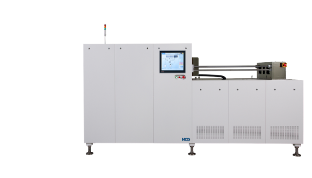
NCD has recently signed a contract to supply ALD equipment for manufacturing high efficiency PERC cells with JA Solar, a large solar cell manufacturer in China. This equipment is Lucida GS Series that offers higher efficiency to crystalline silicon solar cells by depositing high quality Al2O3 ALD thin films on the back side of wafers. 
 
Lucida GS Series is a batch type ALD deposition system that forms backside passivation of Al2O3 on multiple wafers and can process more than 4.500 wafers (@ 6nm thickness) of 156mm x 156mm size per an hour. By applying Lucida GS Series in the production of solar cells, customers can dramatically lower the production cost of high efficiency solar cells due to the high-volume productivity, high yield, efficient gas consumption and low maintenance cost compared to competitors. Based on these advantages and excellence, NCD is confident that the Lucida GS Series will become essential equipment for ALD process application for manufacturing high efficiency solar cells.

NCD will continue to make efforts to become the world’s best specialized company that leads ALD technologies in the future.
< Lucida GS Series >


Spatial atomic layer deposition for coating flexible porous Li-ion battery electrodes

Here is important step forward in fast roll to roll processing of Li-battery electrodes using fast spatial ALD from CU Boulder, Colorado. Spatial ALD (SALD) is based on separating the precursors and inert gas purges in space rather than in time and therefore the deposition rates up to a hundred times faster are achievable. SALD can be performed at ambient atmosphere and therefore is a cheaper technology due to less need of expensive vacuum technology compared to conventional low pressure ALD.

High speed and low cost of ownership opens the door to high volume manufacturing of bulk quantities of energy materials for applications including solar energy, energy storage, or smart windows. Previously ALD Nanosolutions has announced a Spatial ALD technology for conformal encapsulation of ALD on powder material like for instance Li-battery cathode powder (LINK). A good overview of Spatial ALD for energy applications is this review paper by David Muñoz-Rojas et al: "Spatial Atomic Layer Deposition (SALD), an emerging tool for energy materials. Application to new-generation photovoltaic devices and transparent conductive materials" https://doi.org/10.1016/j.crhy.2017.09.004 [OPEN ACCESS]

Please find the JVSTA abstract below for the recent article form Boulder:

Thursday, February 8, 2018

Recent Solar Cell and Battery Materials Articles in JVSTA

Quite a bunch of interesting ALD papers in JVSTA!


Laser ablation compatible substoichiometric SiOx/SiNy passivating rear side mirror for passivated emitter and rear thin-film crystalline silicon solar cells,  Félix Gérenton, Fabien Mandorlo, Erwann Fourmond, Marine Le Coz, Danièle Blanc-Pélissier, Mustapha Lemiti |  Read More


Plasma-enhanced atomic layer deposition of vanadium phosphate as a lithium-ion battery electrode material,  Thomas Dobbelaere, Felix Mattelaer, Philippe M. Vereecken, Christophe Detavernier |  Read More


Performance and durability of broadband antireflection coatings for thin film CdTe solar cells,  G erald Womack, Piotr M. Kaminski, Ali Abbas, Kenan Isbilir, Ralph Gottschalg, John Michael Walls |  Read More

Application of microcracked columnar TiO2 thin films deposited by DC hollow cathode plasma jet in dye-sensitized solar cells,  Roman Perekrestov, Pavel Kudrna, Stanislav Danis, Milan Tichý, Igor Bieloshapka, Rodica Vladoiu |  Read More

Optimizing AlF3 atomic layer deposition using trimethylaluminum and TaF5: Application to high voltage Li-ion battery cathodes,   David H. K. Jackson, Masihhur R. Laskar, Shuyu Fang, Shenzhen Xu, Ryan G. Ellis, Xiaoqing Li, Mark Dreibelbis, Susan E. Babcock, Mahesh K. Mahanthappa, Dane Morgan, Robert J. Hamers, Thomas F. Kuech |  Read More

Single vacuum chamber with multiple close space sublimation sources to fabricate CdTe solar cells,  Drew E. Swanson, Jason M. Kephart, Pavel S. Kobyakov, Kevin Walters, Kevan C. Cameron, Kurt L. Barth, Walajabad S. Sampath, Jennifer Drayton, James R. Sites |  Read More

Spatial atomic layer deposition on flexible porous substrates: ZnO on anodic aluminum oxide films and Al2O3 on Li ion battery electrodes,   Kashish Sharma, Dmitri Routkevitch, Natalia Varaksa, Steven M. George |  Read More
 
Atomic layer deposition of tin oxide using tetraethyltin to produce high-capacity Li-ion batteries,  Denis V. Nazarov, Maxim Yu. Maximov, Pavel A. Novikov, Anatoly A. Popovich, Aleksey O. Silin, Vladimir M. Smirnov, Natalia P. Bobrysheva, Olga M. Osmolovskaya, and Michail G. Osmolovsky, Aleksandr M. Rumyantsev |  Read More

Atomic layer deposition of NiS and its application as cathode material in dye sensitized solar cell,   Neha Mahuli, Shaibal K. Sarkar |  Read More

Effect of the cadmium chloride treatment on RF sputtered Cd0.6Zn0.4Te films for application in multijunction solar cells,  Tushar M. Shimpi, Jason M. Kephart, Drew E. Swanson, Amit H. Munshi, Walajabad S. Sampath, A. Abbas, John M. Walls |  Read More

Wednesday, February 7, 2018

CRITICAL EVENT FOR SEMI MATERIALS - April 26-27 Phoenix

The Critical Materials Council (CMC) Conference is a 2-day event, happening April 26-27 in Phoenix, AZ, providing actionable information on materials and supply-chains for current and future semiconductor manufacturing. Speakers from CMC Members such as GlobalFoundries, Intel, Samsung, and TI, along with analysts and experts from OEMs and materials-suppliers will explore issues associated with using materials such as cobalt and ruthenium in commercial fabs. Evening receptions and lunch allow for networking time with industry leaders.

Keynote speaker David Bloss, VP of Technology and Manufacturing Group, and Director of Lithography Technology Sourcing in Global Supply Management, Intel Corp., will start the three-session event exploring:

* Updates on market dynamics and government regulations,
* Trends in the profitable control of all fab materials, and
* Technology forecasts for future critical materials.

Join us in the Phoenix area: http://cmcfabs.org/cmc-events/


Tuesday, February 6, 2018

ASD 2018 Call for Abstracts Deadline Extended to March 5


Call for Abstracts
Extended to March 5, 2018


The principal chemical processes and mechanisms that enable Area Selective Deposition (ASD) are rapidly becoming critical in several areas of materials and technological advancement. Most notably, the semiconductor industry will likely need new ASD processes to enable “chemical alignment” to complement traditional physical alignment (i.e. lithography) to allow transistors to scale to less than 10 nm dimensions. Other fields are also exploring chemical selectivity in materials to achieve precise targeted performance. Catalytic materials, for example, which are commonly employed to promote chemically selective reactions, are now being designed and constructed using site-selective deposition reactions. In addition, the growing complexity of energy generation and storage materials are also driving the need for new site- or area-selective processes to control heterogeneous material structures.

To share advances in these areas, the 3rd Area Selective Deposition Workshop (ASD 2018), will be held on April 29 – May 1, 2018, at North Carolina State University in Raleigh North Carolina USA. The Workshop will bring together leading international scientists and engineers from academia and industry from all regions to share results and insights into: 1) fundamental principles and barriers to area selective deposition; 2) technological needs and challenges of ASD; 3) new chemical approaches and processes to address the expanding needs; and 4) surface characterization techniques and metrology innovation for ASD.

Based on successful workshops at the Eindhoven University of Technology in 2017 and at IMEC in Leuven Belgium in 2016, ASD 2018 will consist of two days of presentations and discussions, preceded by a welcome reception at North Carolina State University on April 29. The program will include a series of invited and contributed speakers, a panel discussion, as well as a poster session reception on the evening of April 30.

Thursday, February 1, 2018

Invited speakers and tutorials for AVS ALD & ALE 2018 in Incheon Korea

The invited speakers and tutorials for AVS ALD & ALE 2018 in Incheon Korea have been announced! Please follow the link here for full details (LINK). A lot of experts from the South Korean ALD Industry and Fabs will present, including offcourse the early industry adopters (DRAM!) Samsung Electronics and SK Hynix as well as suppliers like Wonik IPS and UP Chemical and a good mix of the worlds best experts will be there as well ALD and ALE. Noting also that there will be multiple presentations from Japan for ALE like Sony (cool!), Toshiba and Tokyo Electron.

As for other years the exhibition has been sold out but sponsoring is open!

SUBMISSION for abstarcts deadline is also close - February 16, 2018 (LINK)


2nd HERALD.ECI Workshop with hands-on training for “bonding HERALD.ECIs from ideas to proposals”

Following the HERALD.ECI network kick-off : June 14, 2017 in Linköping, Sweden, and the 1st HERALD.ECI Workshop on Career Development : August 28-29, 2017 in Ghent, Belgium

The team behind HERALD ECI wisheds you alls a Warm Welcome to the 2nd HERALD.ECI Workshop with hands-on training for “bonding HERALD.ECIs from ideas to proposals” March 1-2, 2018 in Barcelona.

The 2nd HERALD.ECI Workshop is organized by:
  • Mariona Coll & Jaume Gazquez, Institut de Ciència de Materials de Barcelona;
  • Maximilian Gebhard, Ruhr-University Bochum; and
  • Marcel Junige, Technische Universität Dresden.

Just recently the Agenda was released (see below). Please visit the web page administrated by Marcel Junige for more informations : LINK


Picosun establishes a new business unit to ensure the best customer experience

ESPOO, Finland, 1st February, 2018 – Picosun Group, a leading supplier of advanced industrial Atomic Layer Deposition (ALD) thin film coating technology, has established a new business unit dedicated to customer experience. The goal of the new unit is to reinforce and streamline Picosun’s service and support operations even further, to ensure always the highest level customer satisfaction and maximized uptime of PICOSUN™ production ALD systems around the world.


Timo Malinen (right) - The newly appointed Customer Experience Director of the Picosun Group and the leader of the new service business unit in Helsinki and Jonas Sundqvist (left) during the making of the "Picosun - MECRALD technology by Hitachi High-Technologies and Picosun" promotion movie in Helsinki (LINK)

In the last few years, Picosun has become the ALD technology provider of choice for the world’s leading semiconductor manufacturers and various other industries. This is manifested by the impressive 68 % increase in new orders in the calendar year 2017, compared to the previous calendar year, resulting in total value of 24,4 M€ (of new orders). The demand for the company’s industrial ALD solutions is growing fast, and repeat sales of PICOSUN™ P-series high throughput batch ALD tools and PICOPLATFORM™ vacuum cluster systems underline the need for a strong, well-oiled service organization able to provide all-inclusive round-the-clock response around the globe, every day of the year.

Sunday, January 28, 2018

Atomic Layer Deposition (ALD): Basic Principles, Characterizations, and Applications

Thursday, March 15, 2018, 1:00-5:00 p.m. (EDT)

The AVS Short Course Webinar focusing on on Atomic Layer Deposition (ALD) will be held on Thursday March 15 at 1:00 PM eastern time. This webinar will be taught by AVS Instructor, Robert K. Grubbs. Dr. Grubbs has been working in the field ALD for 20 years and has applied the ALD process to solve myrid technical challenges in the semiconductor industry and in the area of national security (Principal Member of the Technical Staff at Sandia National Laboratories).
 
This webinar on Atomic Layer Deposition (ALD) is for anyone who wants to know specific details about how the ALD process works and how to implement ALD in a laboratory setting. The webinar will cover the basic aspects of the chemical mechanism of ALD and how that leads to the unique and potent properties of an ALD process. Multiple examples of ALD chemistry will be covered as well as reactor design, chemical precursor properties, plasma ALD, and molecular layer deposition (MLD).

Registration: LINK


Saturday, January 27, 2018

Scaling proven for embedded Super Fast Non-volatile Memory from Dresden

Ferroelectric hafnium oxide and related materials have been developed in Dresden, Germany for over 10 years now. At the IEDM2017 in December Globalfoundries Fab1 and their partners (NaMLab, Fraunhofer and Ferroelectric Memory GmbH) presented their latest results using the Fab1 22nm FDSOI technology with embedded NVM cells embedded as adopted "standard" high-k / metal gate stacks in the front end process module as so called FeFETs.

Previously much of the work was based on Globalfoundries Fab1 28 nm technology so the move to 22 nm really proves that scalig is back to ferroelectric memory technologies as shown on LinkedIn by Prof. Mikolajick (NaMLab) below.. Since the high-k (doped HfO2) is deposited by ALD this technology is scalable also for FinFETs so don´t be surprised if Globalfoundries would soon present also FeFinFETs.

A FeFET based super-low-power ultra-fast embedded NVM technology for 22nm FDSOI and beyond

IEEE Xplore: 25 January 2018 DOI: 10.1109/IEDM.2017.8268425  

Abstract: We show the implementation of a ferroelectric field effect transistor (FeFET) based eNVM solution into a leading edge 22nm FDSOI CMOS technology. Memory windows of 1.5 V are demonstrated in aggressively scaled FeFET cells with an area as small as 0.025 μm2 At this point program/erase endurance cycles up to 105 are supported. Complex pattern are written into 32 MBit arrays using ultrafast program/erase pulses in a 10 ns range at 4.2 V. High temperature retention up to 300 °C is achieved. It makes FeFET based eNVM a viable choice for overall low-cost and low-power IoT applications in 22nm and beyond technology nodes.


Friday, January 26, 2018

Battery Breakthrough Company Feature - ALD NanoSolutions

There is an ongoing boom in the materials supply chain industry to supply the Electrical Vehicle (EV) manufacturers with battery materials. There are a number of concerns in the supply of the actual materials (e.g. lithium, cobalt and graphite). The technological aspects are also still broad,  however it seems very likely that ALD will play a role for some of the technologies for producing future lithium batteries that we will use in basically all devices ranging from communication (smart phones) and for transportation (cars, trucks, trains, ships, airplanes etc.). 

Alumina ALD Coating on LiCoO2 cathode particles showing a clear improvment in battery cyclability. The ALD coated material (red) shows improved capacity retention compared to uncoated (black). (ALD Nano)

ALD Nano in Boulder Colorado is the pioneer in this technology area and has recently announced scaling up their technology to run high volume of powder (3000 kg/day). They have developed a Spatial vibrationg technology refered to as Continious Vibrating Reactor - CVR.

The scientific, process development and engineering teams at ALD Nano have spent considerable resources over the past few years rapidly developing this first-of-its-kind technology from research scale, bench-top to the current commercial-scale systems. A continuous vibrating reactor, or CVR, provides ALD coating capacity of more than three tons per day and 1,200 tons per year of particle materials. These techniques gained from equipment development open up new pathways for ALD Nano's growth. The CVR is a spatial ALD reactor system and can also be utilized for MLD techniques, run at atmospheric or pressurized conditions, and fitted with various features such as plasma. [LINK]

It seems to me that their technology is mature for high volume manufacturing of powder materials and that they "simply" by scaling the number and/or the size of plants can supply the know how and hardware for full scale production for any big player in the battery materials supply chain. 


ALD Nano was recently highlighted by the Colorado Cleantech Industries Association (CCIA) and here is the information given by their CEO, Wayne Simmons:

Battery Breakthrough Company Feature: ALD NanoSolutions

CCIA [LINK] : We asked several companies “What are the critical changes in the battery industry landscape that will have a strategic impact on your success?” This week, we’re highlighting ALD NanoSolutions.

Wayne Simmons, CEO

Lithium ion batteries for electric vehicles, consumer electronics, and distributed energy storage, along with new versions of lead acid batteries for vehicle start-stop fuel efficiency strategies, are driving today’s growth in the battery energy storage market. Longer term, grid-scale batteries will generate a large impact too. Overall, the dramatic changes and expansion of the battery industry are creating huge new materials markets. Every major chemical and advanced materials company in the world is attracted to this opportunity. However, for new devices like EVs to take meaningful market share, the materials for electrodes, electrolytes, and other battery components need to be engineered at the nanometer, or even atomic, scale. It is this demand for engineering new materials that improve energy storage, safety, and power management metrics, combined with the desired cost stack of inputs to the final battery price, that has a big impact on ALD Nano’s business. The key for us to succeed is to enable the new battery materials with atomic layer deposition technologies that not only solve various technical challenges to reach performance metrics, but can also scale at very low cost.
About ALD NanoSolutions  ALD NanoSolutions (ALD Nano) is creating cost-effective advanced materials through its unique portfolio of atomic layer deposition technologies to transform industries.


Beneq expands in Coating Services

Erik Østreng to lead the new Coating Services business unit 

Beneq, the leading global supplier of atomic layer deposition (ALD) equipment and thin film coating services, and world's premier manufacturer of thin film electroluminescent displays, today announced further investments in ALD coating services and outsourced thin film coating production and the appointment of Erik Østreng as Head of Coating Services.

 
Dr. Erik Østreng (33) has been appointed to lead Beneq’s new business unit for coating services. He will be responsible for the business result and development of the Beneq Coating Services business unit in alignment with Beneq’s strategy, with a focus especially on improving the offering of the coating services unit and expanding the outsourced thin film production model to new application areas.

Coating Services seen as a major growth area

Beneq’s Coating Services business unit offers turnkey production solutions for thin film coatings based on Atomic Layer Deposition (ALD) in Beneq’s Espoo factory, the Home of ALD.

The growing interest from the customers towards the outsourcing solutions is now driving further investments in the area. Growth is expected in many industries, from anti-tarnish coatings for silver and anti-corrosion protection of electronic components and machine parts, to optical coatings and moisture barrier solutions for sensitive electronics, such microdisplays and PCB’s.

Combined with Beneq’s Thin Film Development Services that offer outsourced thin film R&D services, the Beneq Coating Services business unit provides a one-stop solution for companies looking for new ways to improve their products with ALD coatings, from the first ALD samples and coating chemistry research to production pilots and full-blown ALD manufacturing.

Full article: LINK
 

Thursday, January 25, 2018

High Dielectric Constant Materials for Nanoscale Devices and Beyond

Here is a nice review on the introduction of high-k materials in the semiconductor industry and a future outlook by Prof. Hiroshi Iwai at Tokyo and Prof. Akira Toriumi Institute of Technology and their partner Prof. Durga Misra at New Jersey Institute of Technology. Thank you for sharing this one Rob Clark! The paper is part of a winter special issue in Interface (by ECS) with focus on "Importance of dielectric science"  and is free for download.


The authors conclude that:
  • The step coverage advantage of atomic layer deposition (ALD and is possible for, high‑k migration to FinFET CMOS technology.
  • The use of high‑k on new semiconductor substrates such as III-V, Ge and 2D materials is currently being investigated and faces many challenges. 
  • The discovery of ferroelectric properties of HfO2 makes it viable for more potential applications.


High Dielectric Constant Materials for Nanoscale Devices and Beyond
Hiroshi Iwai, Akira Toriumi and Durga Misra

Electrochem. Soc. Interface Winter 2017 volume 26, issue 4, 77-81

Abstract: Tremendous progress of CMOS integrated circuits have been conducted by the down-scaling or the miniaturization of MOSFETs (Metal Oxide Semiconductor Field Effect Transistors). Ten years, ago, the huge direct-tunneling gate leakage current through the thin gate SiO2 film of 1 nm thickness made it impossible to further scale-down the MOSFETs, and replacing the SiO2 by HfO2-based higher-dielectric constant (high-k) material was the solution. In this paper, the history of high-k gate insulator film development and two topics from recent research results regarding ferroelectricity and reliability are described.

Tuesday, January 23, 2018

CMC Conference 2018 Keynote by Intel Litho VP

Register now for early-bird rate to April 24-25 event in Phoenix area
SAN DIEGO, Jan. 23, 2018 /PRNewswire-iReach/ -- TECHCET CA—the advisory service firm providing electronic materials information—and the Critical Materials Council (CMC) of semiconductor fabricators announce that David Bloss, Vice President of Technology and Manufacturing Group, and Director of Lithography Technology Sourcing in Global Supply Management, Intel Corporation, will provide the keynote address at the next CMC Conference to be held April 24-25, 2018 in Chandler, Arizona (http://cmcfabs.org/cmc-events/). Building on the success of the prior CMC Conferences, the 2018 event will feature presentations by technologists from leading fabs, OEMs, materials suppliers, and analysts.


Following the annual members-only CMC meeting held earlier in the week, the 2017 CMC Conference is open to the public. Business drives our world, but technology enables the profitable business of manufacturing new semiconductor devices, and new devices need new materials. Presentation sessions will focus on the following topics:
  • Global Issues & the Supply Chain,
  • Immediate Challenges of Materials & Manufacturing, and
  • Emerging Materials Challenges.
To register for the conference at the early-bird rate of $375 by March 15, 2018—after which the price increases to $450—please got to the website http://cmcfabs.org/registration/.

ABOUT CMC:  The Critical Materials Council (CMC) of Semiconductor Fabricators (CMCFabs.org) is a membership-based organization that works to anticipate and solve critical materials issues in a pre-competitive environment. The CMC is a unit of TECHCET.

ABOUT TECHCET:  TECHCET CA LLC is an advisory service firm focused on process materials supply chains, electronic materials technology, and materials market analysis for the semiconductor, display, solar/PV, and LED industries. Since 2000, the company has been responsible for producing the SEMATECH Critical Material Reports, covering silicon wafers, semiconductor gases, wet chemicals, CMP consumables, Photoresists, and ALD/CVD Precursors. For additional information about these reports or CMC Fabs membership please contact Diane Scott at info@cmcfabs.org +1-480-332-8336, or go to www.techcet.com or www.cmcfabs.org.

Media Contact: Lita Shon-Roy, TECHCET CA LLC, 1-480-382-8336, info@techcet.com

Monday, January 22, 2018

Imec present roadmap down to 20 Ångström logic devices

From now on I think that it is time to start using Ångström instead of Nanometer (nm) when talking about leading edge CMOS and Memory.  At SEMI:s ISS 2018 (Industry Strategy Symposium) last week Luc van den Hove, Chief Executive Officer and President of Interuniversity MicroElectronics Center (IMEC) presented their roadmap for what future Logic nodes might look like going down to 2 nm that is 20 Ångström.

Key interconnect technologies named "scaling boosters" to reach down to 2 nm may be :
  • Continued scaling of self-aligned contacts
  • Cobalt "Super Via" 20 nm wide
  • Burried Ruthenium Rails only 10 nm wide, which seems to be a evolution of the tungsten burried Word Lines and Bitlines introduced by Qimonda for DRAM (65nm in 2009) except offcourse these rails are burried in a dielectric which will  make it stackable. 


Imec Logic roadmap and technologies, Picture from Twitter (LINK)


Besides the interconnect technologies the presentation showed evolution from FinFETs to nanowire FETs and Imecs latest technology development in 300 mm wafer processing technology:
  • Introduction of triple pattering (Much More ALD!)
  • EUV Litography and the introduction Carbon Nano Tube CNT Pellicle for EUV mask protection
  • Smoothening technology in patterning like Atomic Layer Etching for improving the local critical dimension uniformity (LCDU) down from 2.7 to 1.4 nm
In the case of memory technology Imec now focuses on 4 non-volatile types of memory cells besides DRAM and 3DNAND Flash:
  • STTRAM - spin transfer torque magnetoresistive random-access memory
  • RRAM - resistive random-access memory
  • FeRAM - ferroelectric random-access memory (should be renamed DD-RAM for Dresden)
  • SOTRAM - Spin Orbit Torque random-access memory


Sunday, January 21, 2018

The use of ALD in Intel & Globalfoundires leading edge technology

At IEDM 2017 in San Fransisco in December in the Advanced Platform Technologies session Intel and Globalfoundries presented their 10 nm and 7 nm technology, respectively. Intel and Globalfoundries (as well as TSMC) are using different node names, however these two nodes have similar density and can be compared side by side. In a recent article by Scotten Jones in SemiWiki the Intel 10 nm vs. Globalfoundries 7 nm are compared based on previous disclosures, interviews and the IEDM 2017 papers.

This is a very interesting article for those of you who like to dig in deeper into the most leading edge technologies in production 2018 and you can imagine that none of this would have been possible without ALD:
  • Both Intel and Globalfoundries are using SAQP for the fins patterning, presumably using PEALD liners that are on offer from ASM International, Applied Materials and others.
  • Intel is using its fifth generation of high-k metal gates (HKMG). As you know, Intel introduced HKMG in 2007 at 45 nm ahead of the rest of the industry. Whereas Globalfoundries is at its 4th generation, depending on how you count. The IBM Alliance started of with MOCVD High-k (Tokyo Electron at AMD/Globalfoundries and Applied Materials at STMicro) for 32 nm and then moved to ALD high-k (ASM Pulsar 3000) and I am assuming still uses that ALD work horse.
  • In the case of Intel, the contact metal stack also includes a conformal titanium layer and it remains to be seen if this is possibly an ALD process - we know that Prof. Winter has showed amazing progress in thermal ALD of Ti-rich layers, but this could as well be PECVD if the thermal budget allows or some sneaky trics from the Applied Materials PVD magicians in Santa Clara.
  • In the case of Cobalt, we have to assume that the Intel Cobalt vias and lines are not realized by CVD. They are most probably deposited by a Electroless Deposition (ELD) process. ELD Cobalt is claimed to provide void-free bottoms-up pre-filling of vias and contacts as presented by Imec and Lam Research (Solid State Technology LINK) some time ago. In case of the Cobalt liners and Caps used to encapsulate the copper vias and lines by both Intel and Globalfoundries it is safe to assume that these are CVD processes using Applied Materials Cobalt CVD chambers (Endura Volta LINK). Here we know about published work from ALD Cobalt and selective ALD Cobalt that may or may not have come into play (Marissa Kerrigan et al Chem. Mater., 2017, 29 (17), pp 7458–7466)
  • Further up in the Copper layers, the Globalfoundries technology also offer MIM Capacitors that can be either for decoupling or potentially also include embedded DRAM memory cells in a via integration. These have in many cases in older nodes been realized by using low thermal budget ALD or PEALD ZrO2 node dielectric (e.g. from STMicro, Renesas).
  • Adding to all this, there are a multitude of liners, diffusion barriers as well as multiple patterning in BEOL where ALD may have come into play. It is safe to assume that for each node there is more ALD in play.
These speculations are open for debate! :-)

IEDM 2017 - Intel Versus GLOBALFOUNDRIES at the Leading Edge 

by Scotten Jones Published on 12-22-2017 08:00 AM

Article: LINK

Intel 10 nm vs. Globalfoundries 7 nm Fins beautifully conformally coverd by ALD High-k/Metal Gate stacks (SemiWiki).
 

Saturday, January 20, 2018

Hafnium product breakthrough consolidates Dubbo Project business case

Alkane - Hafnium product breakthrough consolidates Dubbo Project business case.

Summary
  • Alkane’s wholly owned subsidiary, Australian Strategic Materials Ltd (ASM), has developed high‐purity hafnium dioxide products tailored to meet market requirements.
  • Hafnium oxide exceeding 99.8% HfO2, and 99.9% (Hf+Zr)O2, has been produced using a proprietary process to separate hafnium from zirconium at the demonstration pilot plant at ANSTO.
  • Over the past 12 months, ASM has consulted extensively with industry to confirm growing market demand for high‐purity hafnium, which currently depends on supply from the production of zirconium metal for specialty alloys and the nuclear industry.
  • Global shortage of hafnium anticipated as demand is poised to outstrip current supply.
  • Hafnium metal for super alloys is currently trading in a US$800 ‐ $900/kg range. The ASM business case assumes a conservative product price of US$500/kg for its oxide.
  • ASM will initially produce 25tpa hafnium to meet projected market demand, ramping up to higher quantities as required.

Download : Download (PDF, 718KB)

Development of high‐purity hafnium dioxide

Australian Strategic Materials Ltd (ASM), a wholly owned subsidiary of Alkane Resources, has successfully developed a high‐purity hafnium dioxide (HfO2) product that will be directly marketable as a feed material for a number of downstream applications and for producing metallic hafnium. The technical specifications of this material have been tailored to meet global market requirements, following extensive industry consultation over the past 12 months. 

Metallic hafnium is the fastest growing market for hafnium and the most significant by volume, particularly due to the use of hafnium in superalloys and other aerospace alloys. The usual precursor is hafnium dioxide, which needs to be recovered from zirconium metal production streams. The high purity hafnium dioxide developed by ASM exceeds 99.8% HfO2, and 99.9% (Hf+Zr)O2, providing the ideal feedstock for the high‐purity metallic hafnium that is in demand for alloying purposes. A high purity hafnium chemical precursor has also been developed.

The new products were produced by a proprietary process at ASM’s Demonstration Pilot Plant at the Australian Nuclear Science and Technology Organisation (ANSTO) in Sydney, New South Wales. The process flowsheet for the Dubbo Project consists of a sulphuric acid leach followed by solvent extraction recovery and refining to produce several products, including zirconium, hafnium, niobium and rare earths. The process pathway to recover hafnium was developed in 2015 and proved during 2017, and allows the flexible recovery of high‐purity hafnium dioxide from the high‐purity zirconium stream.

The development of this high‐purity hafnium dioxide material demonstrates the ability of ASM to produce a highly marketable hafnium product out of the Dubbo Project. ASM will continue to work with industry to secure offtake agreements and develop further enhanced products, with the view to establishing a customer base for hafnium products ahead of plant commissioning.


Hafnium market and outlook for future growth

Global demand for hafnium is rising particularly for use in metallic form, which currently accounts for around 85 per cent by volume (60% superalloys, 15% plasma cutting tips, 10% nuclear control rods). Emerging aerospace applications are expected to consume further significant volumes of metallic hafnium. Hafnium dioxide is meanwhile emerging as a material of choice in semiconductors and data storage devices (ferro‐electric applications), while many future industries such as those based on its thermo‐electric properties and super high temperature ceramics for supersonic aircraft and space vehicles will also rely on materials containing hafnium.

Projected growth in demand is poised to exceed current production, which is limited to about 70tpa (83tpa HfO2), since hafnium is typically only extracted from zirconium processing streams for nuclear energy applications requiring high‐purity zirconium. Market research by ASM and independent international market consultants forecasts a 2026 base demand of 112tpa (132tpa HfO2), and an unconstrained high‐demand case of 151tpa (178tpa HfO2).
 
 
The Project represents a unique source of hafnium that is independent of all traditional markets – including China (currently accounting for at least 75% of world production of zirconium materials, and over 95% of zirconium chemicals), the nuclear zirconium industry and the zircon industry in general. To ensure a sustainable business case, the ASM processing plant will undergo staged ramp‐up in production volumes to keep pace with world demand. Start‐up volumes will be around 25tpa hafnium metal (30tpa HfO2), increasing in line with market growth; full plant capacity is conservatively estimated at 200tpa.

Hafnium product pricing remains opaque due to security issues and limited production but the metal for super alloys is currently trading in a US$800 ‐ $900/kg range. The ASM business case assumes a conservative product price of US$500/kg for its oxide.