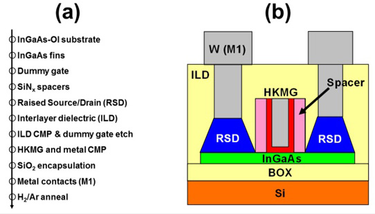
Showing posts with label High-k. Show all posts

Wednesday, January 27, 2016

IBM Research present InGaAs on insulator FinFET process using Plasma Enhanced ALD HKMG

IBM Research GmbH in Switzerland has developed an n-channel indium gallium arsenide (InGaAs) on insulator fin field-effect transistor (FinFET) process and claims the highest on-current to date for CMOS-compatible InGaAs devices integrated on silicon (Si) [Vladimir Djara et al, IEEE Electron Device Letters, published online 1 January 2016].

According to the paper, the devices were fabricated using a replacement metal gate (RMG) flow, including ultra-thin SiN spacers, scaled high-k/metal gate (HKMG), and highly-doped raised source and drain (RSD) modules for improved electrical performance.

ALD Inside:
  • 12-nm-thick SiN spacers were deposited by plasma-enhanced atomic layer deposition (PEALD)
  • After dummy gate removal, a HKMG, featuring a scaled Al2O3/HfO2 dielectric stack with a capacitance equivalent thickness (CET) of ∼1.5 nm, was deposited using a highly conformal and uniform PEALD process. the process has previously been published here.  The tool used is a FlexAL ALD from Oxford Instruments and the PEALD processes are TMA and O2 plasma for Al2O3 and TEMAH and O2 plasma for HfO2.
The FlexAL® systems provide a new range of flexibility and capability in the engineering of nanoscale structures and devices by offering remote plasma atomic layer deposition (ALD) processes and thermal ALD within a single ALD system.

Pretty cool if you ask me to see that PEALD is used for gate dielectric, which is usually not the case on silicon channels where thermal HfCl4/H2O process is dominating and also that TEMAHf can perform this good as a gate dielectric. Please read the full report in Semiconductor Today here.

Tuesday, January 19, 2016

A Non-FinFET Path to 10nm Globalfoundries’ FD-SOI Alternative

STMicroelectronics and CEA/Leti have been leading an effort in scaling FD-SOI for long now and have recently gotten some muscles in support by fabing it at Samsung (28nm) and Globalfoundries Fab1 in Dresden (22nm). I ran some sub 22 nm development LOTs for one of our customers some years ago and form an ALD high-k point of view this was a a piece of cake. I gave them the same recipe, adjusted the thickness slightly, as the other guys and they didn't complain. That is why I since then always follow news on FD-SOI - it´s such an underdog technology compared to bulk FinFET in terms of ecosystem support and investments but I like underdogs - or  maybe rather medium sized dogs with a big dog attitude. Anyhow here is a recent feature article by GloFo on the topic that is worth reading:

It was the coolest transistor development in many a year. Rather than continually squishing transistor parts closer and closer together, we flipped it to vertical and celebrated the arrival of the FinFET.


Image courtesy GlobalFoundries

Which was great: it gave us a way to keep increasing performance in many of the applications where the value lies in the speed of the circuit. But after the initial party was over and we started picking up the pointy party hats and nursing the hangovers with massive doses of ibuprofen, we started looking at the bill. FinFET is nice, but it’s also expensive. And, while we’re throwing stones, it’s also not so great for analog and RF designers based on the quantized nature of the gate. You can’t increase channel dimensions by 1.5 times; it’s either 1 or 2.

Rutger Wijburg announcing the investment for 22 nm FD-SOI investment at Fab1 in Dresden, Germany. (Picture by Computer-Oiger)


FinFET has been billed as the future of silicon, and Intel jumped on it, meaning everyone else had to as well. But that pounding morning-after headache is pretty strong, and there are folks wishing they had an alternative to FinFET.

Monday, December 14, 2015

Imec Boosts Performance of III/V Devices using Novel ASMi ALD HKMG Stack

Imec presented a high performing gate-all-around InGaAs Nanowire FETs (Lg=50nm) at IEDM 2015. Imec succeeded in increasing the performance by gate stack engineering using a novel gate stack ALD inter-layer (IL) material developed by ASM, and high pressure annealing. The novel IL/HfO2 was benchmarked to the typically used Al2O3/HfO2 stack.

TEM of complete gate-all-around InGaAs Nanowire FET and HRTEM of the gatestack. The insert shows a close up of the Interface Layer HKMG developed and presumably deposited by ASM on any of the ASM ALD chambers available at imec - I am assuming that the high-k was deposited in a Pulsar 3000 and the TiN cap in a ASM A412 Large Batch ALD Furnace and I have absolutely no clue what the ALD inter layer may be - obviously it has less electrons than HfO2.

Monday, December 7, 2015

ASMi to host Technology Seminar at IEDM with Dina Triyoso from Globalfoundries

ASM International, the leading supplier of ALD deposition tools for leading edge Logic and Memory technologies is as usual hosting a Technology Lunch Seminar at IEDM that is taking place this week in Washington. This time they have invited Dina Triyoso from Globalfoundries to give a talk on

'Architectural choices and material challenges for future electronics'. Dina has a very strong background in ALD, High-k/Metal Gate, MIM capacitors and ALD for spacer technologies so this will certainly be a fantastic opportunity to learn about the latest from a true expert in the field.


ASM International N.V. (Euronext Amsterdam: ASM) today announces that it will host a technical luncheon seminar in Washington DC, US, on Wednesday, December 9, 2015, the third day of the IEDM Conference.

In this technology seminar, ASM and a distinguished keynote speaker will highlight the challenges and potential solutions for achieving next generation 3D devices.

The agenda is as follows:

11:30 am Food and drinks
12:10-12:20 pm Ivo Raaijmakers (ASM) - Welcome and introduction
12:20-12:50 pm Dina Triyoso (GLOBALFOUNDRIES) -
'Architectural choices and material challenges for future electronics '

Following the presentations, there is an opportunity for open discussion and networking until 1:15 pm.

The ASM technology seminar will take place in the Kalorama room at the Churchill Hotel (across from the Hilton Washington), 1914 Connecticut Avenue NW, Washington DC 20009, US. The room will open at 11:30 am for invited attendees. Interested parties should contact Rosanne de Vries, +31 88 100 8569, rosanne.de.vries@asm.com.

Source: http://www.finanznachrichten.de/nachrichten-2015-12/35815943-asm-international-nv-asm-international-n-v-to-host-technology-seminar-399.htm

Sunday, November 22, 2015

SK Hynix & SNU demonstrate 28nm RRAM cell with ultra thin ALD Ta/Ta2O5 stack

Here is a impressive report by SK Hynix & Prof. Hwang and co-workers SNU on a RRAM device with Ta/Ta2O5 stacked RS layers with ultra-thin Ta2O5 thicknesses (0.5–2.0 nm) deposited by ALD. Woah that´s thin  - like the same order of thickness like native oxide, which makes me wonder if teh extra couple of ALD cycles was needed --> I need to study the paper more carefully!

Thickness effect of ultra-thin Ta2O5 resistance switching layer in 28 nm-diameter memory cell 

C.S. Hwang et al

Scientific Reports 5, Article number: 15965 (2015)
doi:10.1038/srep15965
(a) Schematic diagram and (b) TEM image of the TiN/Ta2O5/Ta/TaN device. Ta2O5 (0.5 nm) device, and (d) Ta2O5 (1.5 nm) device. Insets show the linear I-V plot. Scanning transmission electron microscopy (STEM) high angle annular dark field (HAADF) images of (c) 0.5 nm-thick device and (d) 2.0nm-thick device. 

Resistance switching (RS) devices with ultra-thin Ta2O5 switching layer (0.5–2.0 nm) with a cell diameter of 28 nm were fabricated. The performance of the devices was tested by voltage-driven current—voltage (I-V) sweep and closed-loop pulse switching (CLPS) tests. A Ta layer was placed beneath the Ta2O5 switching layer to act as an oxygen vacancy reservoir. The device with the smallest Ta2O5 thickness (0.5 nm) showed normal switching properties with gradual change in resistance in I-V sweep or CLPS and high reliability. By contrast, other devices with higher Ta2O5 thickness (1.0–2.0 nm) showed abrupt switching with several abnormal behaviours, degraded resistance distribution, especially in high resistance state, and much lower reliability performance. A single conical or hour-glass shaped double conical conducting filament shape was conceived to explain these behavioural differences that depended on the Ta2O5 switching layer thickness. Loss of oxygen via lateral diffusion to the encapsulating Si3N4/SiO2 layer was suggested as the main degradation mechanism for reliability, and a method to improve reliability was also proposed.


Saturday, October 24, 2015

Ferroelectric HfO2 enable giant pyroelectric energy conversion and highly efficient supercapacitors

A new application for energy harvesting and storage of ferroelectric hafnium oxide has been investigated and proven by researchers at NaMLab in Dresden, RWTHA Aachen and TU Munich, Germany. One major advantage of the use of hafnium oxide over other materials is the low cost of fabrication of these films while it has been proven feasible by existing semiconductor process technology like in ALD in CMOS high-k / metal gate and high-k node dielectric for DRAM capacitors.

To summarize this investigation:
  • Ferroelectric phase transitions in Si:HfO2 thin films yield giant pyroelectricity.
  • Si:HfO2 for highly efficient supercapacitors is first reported.
  • Si:HfO2 shows highest figures of merit for pyroelectric energy harvesting.
  • Si:HfO2 for electrocaloric cooling and infrared sensing is first reported.

Ferroelectric phase transitions in nanoscale HfO2 films enable giant pyroelectric energy conversion and highly efficient super capacitors


Temperature- and field-induced phase transitions in ferroelectric nanoscale TiN/Si:HfO2/TiN capacitors with 3.8 to 5.6 mol% Si content are investigated for energy conversion and storage applications. Films with 5.6 mol% Si concentration exhibit an energy storage density of ~40 J/cm3 with a very high efficiency of ~80% over a wide temperature range useful for supercapacitors. Furthermore, giant pyroelectric coefficients of up to −1300 µC/(m2 K) are observed due to temperature dependent ferroelectric to paraelectric phase transitions. The broad transition region is related to the grain size distribution and adjustable by the Si content. This strong pyroelectricity yields electrothermal coupling factors k2 of up to 0.591 which are more than one order of magnitude higher than the best values ever reported. This enables pyroelectric energy harvesting with the highest harvestable energy density ever reported of 20.27 J/cm3 per Olsen cycle. Possible applications in infrared sensing are discussed. Inversely, through the electrocaloric effect an adiabatic temperature change of up to 9.5 K and the highest refrigerant capacity ever reported of 19.6 J/cm3 per cycle is achievable. This might enable energy efficient on-chip electrocaloric cooling devices. Additionally, low cost fabrication of these films is feasible by existing semiconductor process technology.

Thursday, October 22, 2015

Successful industrialization of high-density 3D integrated silicon capacitors for ultra-miniaturized electronic components

Three high-tech SMEs finalize the joint EU-funded PICS project on innovative ALD materials and manufacturing equipment

 
Caen, Oct. 22, 2015 – Two years after the launch of the PICS project (funded by the FP7 funding instrument dedicated to research for the benefit of SMEs), three European SMEs, IPDiA, Picosun and SENTECH Instruments along with CEA-Leti and Fraunhofer IPMS-CNT announce the major technological results achieved during this program. 

Two new dielectric stacks were developed and integrated into the IPDiA 3D trench capacitors by IPDiA, CEA-Leti and Fraunhofer IPMS-CNT. The initial specifications were fulfilled and proven by electrical measurements. A new record on capacitance density (>500nF/mm² at 3.3V) and an extended operation voltage (10V with 150nF/mm²) were obtained, which expands IPDiA’s ability to meet current market requirements particularly in the field of medical or aeronautics. Qualification procedure was initiated during the project by launching preliminary reliability studies and it will continue in the coming months.
 
Read more... (369.11 kB)
 
Prototype of medical pills integrating temperature sensor and RF transceiver


3D trench capacitors integrated into Silicon 
 

Publication Overview

Title of Publication Author(s) Link
Picosun ALD enables a new generation of medical devices Picosun click here 
Innovative ALD materials and tools or high densIty 3D integrated capacitors Fraunhofer IPMS click here
Presentation: NIL industrial Days (19-20 March 2015, Berlin) Pinnow (SENTECH) click here
Presentation: EuroNanoForum (10-15 June 2015, Riga) C. Billard (CEA) click here
Presentation: "Development of innovative ALD materials for high density 3D integrated capacitors” ALD Symposium, SEMICON Europe 2014 (7-9 October 2015, Grenoble) M. Czernohorsky (Fraunhofer IPMS-CNT) click here
Presentation: "Ultra-thin high density capacitors for advanced packaging solutions" 20th European Microelectronics and Packaging Conference & Exhibition (September 13-16, 2015 in Friedrichshafen, Germany) K. Seidel (Fraunhofer IPMS-CNT) click here
Presentation: "HfO2-Al2O3 nanolaminate dielectric for ultra-high integrated MIM capacitors" RAFALD workshop (November 16-18, 2015 Grenoble, France). A. Lefevre click here 
PICS Poster   click here 
 

Saturday, October 3, 2015

IBM Research showcases Carbon Nanotubes (CNT) down to 9nm contact

Here is A breakthrough news from IBM Watson Research Center on integrating CNTs down to 9nm contacts. This section from a recent interview with one of the researchers, Shu-Jen Han, behind this work taken from The IBM Research Blog:


Silicon has offered many advantages as a transistor material for the last half century. One biggest perhaps was that it forms a great gate dielectric – SiO2. It also comes with a very pure and high quality substrate, silicon wafers, to start with. And over time we’ve used other materials and device structures to improve its abilities, such as transitioning to high-k metal gate transistors and FinFETs.

On the other hand, for carbonnanotubes, many material issues have to be solved to obtain similar high-quality carbon nanotube wafers for device fabrication. We can’t switch to an entirely new material over night, but silicon is reaching its scaling limits.
 
 
Dr. Qing Cao and my other teammates at [the IBM Watson Research Center] developed a way, at the atomic level, to weld - or bond – the metal molybdenum to the carbon nanotubes' ends, forming carbide. Previously, we could only place a metal directly on top of the entire nanotube. The resistance was too great to use the transistor once we reached about 20 nm. But welding the metal at the nanotubes' ends, or end-bonded contacts, is a unique feature for carbon nanotubes due to its 1-D structure, and reduced the resistance down to 9 nm contacts. Key to the breakthrough was shrinking the size of the contacts without increasing electrical resistance, which impedes performance. Until now, decreasing the size of device contacts caused a commensurate drop in performance.

For full details on this breakthrough research please see a recently published article in Science:

End-bonded contacts for carbon nanotube transistors with low, size-independent resistance

Qing Cao, Shu-Jen Han, Jerry Tersoff, Aaron D. Franklin, Yu Zhu, Zhen Zhang, George S. Tulevski, Jianshi Tang, Wilfried Haensch

Science 2 October 2015:
Vol. 350 no. 6256 pp. 68-72
DOI: 10.1126/science.aac8006 

Moving beyond the limits of silicon transistors requires both a high-performance channel and high-quality electrical contacts. Carbon nanotubes provide high-performance channels below 10 nanometers, but as with silicon, the increase in contact resistance with decreasing size becomes a major performance roadblock. We report a single-walled carbon nanotube (SWNT) transistor technology with an end-bonded contact scheme that leads to size-independent contact resistance to overcome the scaling limits of conventional side-bonded or planar contact schemes. A high-performance SWNT transistor was fabricated with a sub–10-nanometer contact length, showing a device resistance below 36 kilohms and on-current above 15 microampere per tube. The p-type end-bonded contact, formed through the reaction of molybdenum with the SWNT to form carbide, also exhibited no Schottky barrier. This strategy promises high-performance SWNT transistors, enabling future ultimately scaled device technologies. 

Monday, August 31, 2015

Japanese researchers provide record low Dit in ALD Al2O3/La2O3/InGaAs gate stacks

InGaAs is one of the most promising III/V semiconductor materials for n-channel MOSFETs because of its extremely high electron mobility of ∼13 800 cm2/V s. However, there  is a major issue with InGaAs not having a high quality native oxide like Silicon resulting in a high interface state density at InGaAs MOS interfaces degrades the MOSFET performance because of Ga dangling bonds and/or As-As dimers created during the oxidation process at InGaAs surfaces. It has been reported that the passivation of trivalent oxides such as Gd2O3 or Al2O3 with InGaAs surfaces can eliminate such dangling bonds and dimers because of the abrupt and chemical-bond-well-arranged interface between the trivalent oxides and InGaAs.


TEM image of Au/AlO (3.5 nm)/LaO (0.4 nm)/InGaAs gate stacks. Citation: J. Appl. Phys. 118, 085309 (2015); http://dx.doi.org/10.1063/1.4929650

ALD HfO2 has already been introduced at 45 nm CMOS and is still the dominating high-k material in high performance CMOS including recent Si FinFET technologies. Therefore, many have chosen to combine HfO with the AlO/InGaAs structure by continuously ALD has been employed for CET scaling. Thin CET of ∼1.08 nm and low of ∼5 × 1012 cm−2 eV−1 have been realized in the HfO/AlO/InGaAs gate stacks.

Another high-k that has commonly been used and is used e.g. as a dopant in the IBM Alliance 28 nm planar CMOS technology is LaO, which is also trivalent oxide. It has been shown on InGaAs that La2O3 can further improve the MOS interface quality by the formation of Ga-O-La and In-O-La bonds. [ref]

In a very good study presented below by University of Tokyo, JST-CREST and Sumitomo Chemicals a high quality LaO films were deposited on InGaAs by ALD. It was found that the LaO/InGaAs interfaces provide recorded-low of ∼3 × 1011 cm−2 eV−1 as the InGaAs MOS interfaces, which is attributable probably to the intermixing reaction between LaO and InGaAs. It is concluded, as a result, that the AlO/LaO/InGaAs gate stacks can realize lower than in the conventional AlO/InGaAs MOS interfaces with maintaining small hysteresis and low gate leakage by optimizing the thickness of AlO and LaO.

For me now some questions remains - why not combine the best of the best in one stack, i.e., HfO2/La2O3/InGaAs? Perhaps with only a slight touch of blend with Al2O3. Another question that worries me when reading HKMG InGaAs papers is the very low thermal budget that has to be used.  The first high-k layer is deposited at 150 deg. C not destroy the super sensitive InGaAs interface. Most high-k materials needs to be deposited in the ranger 250 to 300 deg.C in order to perform at its best in addition PDAs or PMAs will bring out even more out of the material. Here and in other studies that I have seen a PMA of only 300 deg. C is used. Just imagine bringing this stack on to a silicon based channel material and it will not perform too much better than old poly/SiON with respect to CET / Leakage performance. I guess in the end it is all about the higher mobility given by a III/V channel. It just hurts every time seeing all these smart guys using a relatively low performing high-k.

Please find the OPEN ACCESS publication below!

Impact of La2O3 interfacial layers on InGaAs metal-oxide-semiconductor interface properties in Al2O3/La2O3/InGaAs gate stacks deposited by atomic-layer-deposition [OPEN ACCESS]

C.-Y. Chang, O. Ichikawa, T. Osada, M. Hata, H. Yamada, M. Takenaka and S. Takagi 
J. Appl. Phys. 118, 085309 (2015); http://dx.doi.org/10.1063/1.4929650


(a) of the AlO (3.5 nm)/LaO/InGaAs gate stacks as a parameter of the LaO ALD cycle numbers, and (b) the LaO ALD cycle number dependence of of AlO (3.5 nm)/LaO/InGaAs at the surface energy of 0.1 eV from midgap ( ). Citation: J. Appl. Phys. 118, 085309 (2015); http://dx.doi.org/10.1063/1.4929650


We examine the electrical properties of atomic layer deposition (ALD) LaO/InGaAs and AlO/LaO/InGaAs metal-oxide-semiconductor (MOS) capacitors. It is found that the thick ALD LaO/InGaAs interface provides low interface state density ( ) with the minimum value of ∼3 × 1011 cm−2 eV−1, which is attributable to the excellent LaO passivation effect for InGaAs surfaces. It is observed, on the other hand, that there are a large amount of slow traps and border traps in LaO. In order to simultaneously satisfy low and small hysteresis, the effectiveness of AlO/LaO/InGaAs gate stacks with ultrathin LaO interfacial layers is in addition evaluated. The reduction of the LaO thickness to 0.4 nm in AlO/LaO/InGaAs gate stacks leads to the decrease in hysteresis. On the other hand, of the AlO/LaO/InGaAs interfaces becomes higher than that of the LaO/InGaAs ones, attributable to the diffusion of AlO through LaO into InGaAs and resulting modification of the LaO/InGaAs interface structure. As a result of the effective passivation effect of LaO on InGaAs, however, the AlO/10 cycle (0.4 nm) LaO/InGaAs gate stacks can realize still lower with maintaining small hysteresis and low leakage current than the conventional AlO/InGaAs MOS interfaces.

Wednesday, August 12, 2015

Rice U. discovery may boost ReRAM memory technology

My favorite high-k metal oxide Ta2O5 is used again for a resistive RAM memory - this time with my least favorite material - Grrrraphene. Just can´t stand the hype I guess. Anyhow considering recent developments in cross bar Memory cell technology by Intel and Micron this could prove to be a future prospect.


A schematic shows the layered structure of tantalum oxide, multilayer graphene and platinum used for a new type of memory developed at Rice University. The memory device overcomes crosstalk problems that cause read errors in other devices. 
(Tour Group/Rice University)

PUBLIC RELEASE: 10-AUG-2015Rice U. discovery may boost memory technology
Rice University scientists make tantalum oxide practical for high-density devices


Scientists at Rice University have created a solid-state memory technology that allows for high-density storage with a minimum incidence of computer errors.

The memories are based on tantalum oxide, a common insulator in electronics. Applying voltage to a 250-nanometer-thick sandwich of graphene, tantalum, nanoporous tantalum oxide and platinum creates addressable bits where the layers meet. Control voltages that shift oxygen ions and vacancies switch the bits between ones and zeroes.

The discovery by the Rice lab of chemist James Tour could allow for crossbar array memories that store up to 162 gigabits, much higher than other oxide-based memory systems under investigation by scientists. (Eight bits equal one byte; a 162-gigabit unit would store about 20 gigabytes of information.)

Details appear online in the American Chemical Society journal Nano Letters. More details can be found here: http://www.eurekalert.org/pub_releases/2015-08/ru-rud081015.php

Monday, August 10, 2015

Ferroelectric HfO2 by ALD Key Breakthrough in ITRS “Beyond CMOS” Update 2015

Following the ITRS Summer Meeting, Palo Alto, CA, July 11-12, 2015 Ferroelectric HfO2 by Fraunofer CNT and NaMLab in Dresden Germany is showcased as a "Key Breakthrough" in the ITRS “Beyond CMOS” Update 2015. You can find this presentation in by ITRS Emerging Research Devices (ERD) amongst others in the excellent new ITRS 2.0 website : http://www.itrs2.net/


Monday, July 27, 2015

Hynix high bandwidth memory in an AMD Radeon ALD High-k Fury

Check it out - this is like the coolest thing I have ever seen so far - the two leading ALD High-k products (DRAM & High performance CMOS) merged into one ultra high performance graphics chip by AMD. TechInsights has investigated the AMD Fury X cards in their lab  and published it in a series of articles in EE Times:

The Hunt for Hynix HBM - Hynix high bandwidth memory addresses bandwidth limitations


Accordingly, SK Hynix announced its high bandwidth memory (HBM) product in early 2014, claiming it to be the world’s first 8Gb module made using 2Gb, 20nm node, DDR4 SDRAM. Now the HBM modules has shown up in product - AMD’s Radeon 390X Fury X graphics card.


According to TechInsight : "Hynix disclosed a via middle process for their HBM in two papers (Electronics Components & Technology Conference 2013 and VLSI Tech. Digest 2014). The TSV openings are formed after the tungsten contacts to the gates and source/drain regions are made, using a Bosch TSV etch. An oxide liner is then deposited along the via sidewalls, lined with a Ta-based barrier and Cu seed layers, and filled with electroplated Cu. A thermal anneal process is used as a Cu stress relief. A CMP and etch process is used to thin the backsides of the DRAM wafer and expose the Cu TSVs. The backsides of the DRAM wafers are then passivated with oxide, followed by the formation of the backside micro bumps."


AMD Radeon Fury X (Source: TechInsights)


Some facts from the reports:

  • The GPU die has four Hynix HBM memory modules arranged around its perimeter. 
  • Both the GPU and the HBM modules are flip-chip bumped to a UMC fabbed interposer. 
  • The interposer is, in turn, bumped to a laminate substrate. 
  • The GPU itself is a massive measuring in at 23mm by 27mm large, and is believed to be fabricated using TSMC’s 28nm HKMG process.


"The GPU die is seen in the center of the module with four Hynix HBM memory modules arranged around its perimeter. Both the GPU and the HBM modules are flip-chip bumped to a UMC fabbed interposer. This interposer is, in turn, bumped to a laminate substrate. The GPU is massive measuring in at 23mm by 27mm large, and is believed to be fabricated using TSMC’s 28nm HKMG process." (EE Times, TechInsight)


Schematic cross section of HBM module. (Source: AMD HBM brochure, TechInsights)


Hynix HBM memory (Source: Package Analysis of the SK-Hynix HBM, TechInsights)


Monday, July 20, 2015

The Ferroelectric Memory Company - FCM from Dresden

The FeFET is a long-term contender for an ultra-fast, low-power and non-volatile memory technology. In these devices the information is stored as a polarization state of the gate dielectric and can be read non-destructively as a shift of the threshold voltage. The advantage of a FeFET memory compared to the Flash memory is its faster access times, much lower power consumption at high data rates, and the easy integration of the device with common high-k metal gate transistors in complementary metal-oxide-semiconductor (CMOS) technology. 

The basics of the idea of a were already laid in the early 2000s in the research department of the memory manufacturer Qimonda. The discovery of ferroelectricity in doped hafnium led there to the registration of several basic patents, which went to NaMLab gGmbH after the Qimonda insolvency.  


In 2013 the proof of principle of a hafnium based ferroelectric field effect transistor (FeFET) memory cell on 28nm technology platform was manufactured at Globalfoundries Fab1 and Fraunhofer CNT in Dresden. There is a hope that the successful commercialization of such an embedded NVM memory technology could have disruptive character.


During the last years the electrical properties of ferroelectric transistors were studied in detail. In the framework of a project together with GLOBALFOUNDRIES and Fraunhofer CNT, which was funded by the Free State of Saxony, silicon doped HfO2 layers were integrated into high-k metal gate transistors in 28 nm CMOS technology. Depending on the polarization state of the ferroelectric gate insulator a memory window in the range of ~1.2 V threshold voltage shift can be reached. Extrapolation of the measured memory window over time indicates a retention time of 10 years with a remaining memory window of 0.4 V. Functional devices with gate length down to ~30 nm were demonstrated.


Today Stefan Müller, Marko Noack and Jörg Andreasas a the team has started The Ferroelectric Memory Company - FCM and currently they are anchored to NaMLab gGmbH and benefits from a The EXIST Research Transfer-financing and support and mentorship by one of the leading semiconductor memory experts Prof. Thomas Mikolajick (Scientific director of NaMLab).


TEM of FeFET processed in 28 nm high-k metal gate CMOS Technology (left) and 2D TCAD-model for device simulation (right). (Picture from NaMLab)


Sunday, July 12, 2015

Thermo Scientific present Angle resolved XPS Metrology solution for ALD High-k Dielectrics

Many of you in the ALD and High-k business have used or are using XPS to analyze high-k material like HfO2 - pure, mixed or doped with other oxides and elements like SiO2, Al2O3, La2O3, Cl, F, ...


I know for sure that XPS is use as a standard metrology method post high-k deposition in many 300 mm fabs. This is not restricted to mapping just blanket monitor wafers but also to measurement directly on product wafers. In advanced logic and DRAM memory this can be done at different positions in the integration flow depending on the technology (High-k first or last or hybrid, DRAM capacitors) - so it is an established method for high-k in production.

Now the gate stack or advanced stacks for various memory devices (e.g. DRAM, RRAM, FRAM) does not really consist of any bulk material anymore - it has come down to be a extremely advanced stack of ultra thin interfaces. Not even the substrate is bulk any more id you think about HALO doping profiles and FD-SOI technology. That it is why it is interesting to read those application paper from Thermo Scientific – Surface Analysis and Microanalysis on mapping High-k wafers using Angle Resolved XPS of 200 mm wafers. I have included some of the information below for the full paper please download it here from the Thermo Scientific application library : Characterization of high-k dielectric materials on silicon using Angle Resolved XPS


Thickness line scan across the diameter of the 200 mm wafer showing the variation of the thickness of the mixed Al2O3 and HfO2 layer and the thickness of the SiO2 interfacial layer.


XPS maps of Al 2p (upper left) and Hf 4f (lower left) from a 200 mm wafer. XPS maps of O 1s. The lower right map is oxygen in a state with a low binding energy (usually associated with hafnium). The upper right map is oxygen in a state with a high binding energy (usually associated with aluminum and silicon). 


Example of a depth profile through a sample HfO2 on SiO2 on Si. The profile was constructed from ARXPS data.

Thermo Scientific Theta Probe and Theta 300 provide essential information for the next generation of gate dielectrics:

• Layer thickness 
• Thickness of the intermediate layer
• Chemical states of the layer and the intermediate layer • Uniformity of the layers
• Distribution of the material within the layer 

ARXPS is non-destructive and avoids the use of sputtering with an ion beam. Sputtering has been shown to alter the composition of the layer and causes atomic mixing both of which can cause a misinterpretation of the data.


Friday, June 12, 2015

Samsung and SNU identifies the next Super High-k

Here is another publication from Samsung on high-k screening in collaboration with Academia. This time in collaboration with researchers from the home base at Seoul National University. This is somehow a new behavior of Samsung who actually withdrew talks in front of ALD 2012 in Dresden on anything realting to high-k and DRAM development and I have not seen that much publishing from Samsung since then on these topics. Calculated results do usually not tend to interest me but this one is very, very interesting and I think it will take me some time to go there it - fully understand I will not.


"Except for c-BeO, we could not find any outstanding high-κ dielectrics with eitherEg or κ larger than those of the HfO2 thin films currently used in CPU or DRAM (Eg~6.0 eV and κ~20–25; see t-HfO2)"


Cubic BeO will probably be a hot ALD topic for the rest of 2015 and I do wonder if Prof. Wang will mention BeO in Portland at the AVS ALD 2015 in Portland when he gives his invited talk: 

Cheol Seong Hwang, Seoul National University
“Capacitor Dielectric and Electrodes for DRAM with sub-20 nm Design Rule”

Check out the paper - it is Open Access - thank you Samsung!

Novel high-κ dielectrics for next-generation electronic devices screened by automated ab initio calculations (Open Access)

Kanghoon Yim, Youn Yong, Joohee Lee, Kyuhyun Lee, Ho-Hyun Nahm, Jiho Yoo, Chanhee Lee, Cheol Seong Hwang and Seungwu Han

NPG Asia Materials (2015) 7, e190; doi:10.1038/am.2015.57
Published online 12 June 2015


The experimental band gap and dielectric constant for well-known oxides. The property region ideal for dielectrics is also shown.


Abstract:
As the scale of transistors and capacitors in electronics is reduced to less than a few nanometers, leakage currents pose a serious problem to the device’s reliability. To overcome this dilemma, high-κ materials that exhibit a larger permittivity and band gap are introduced as gate dielectrics to enhance both the capacitance and block leakage simultaneously. Currently, HfO2 is widely used as a high-κ dielectric; however, a higher-κ material remains desired for further enhancement. To find new high-κ materials, we conduct a high-throughput ab initiocalculation for band gap and permittivity. The accurate and efficient calculation is enabled by newly developed automation codes that fully automate a series of delicate methods in a highly optimized manner. We can, thus, calculate >1800 structures of binary and ternary oxides from the Inorganic Crystal Structure Database and obtain a total property map. We confirm that the inverse correlation relationship between the band gap and permittivity is roughly valid for most oxides. However, new candidate materials exhibit interesting properties, such as large permittivity, despite their large band gaps. Analyzing these materials, we discuss the origin of large κ values and suggest design rules to find new high-κ materials that have not yet been discovered.


Eg vs κ plot for computed structures for 1158 oxides. Each point is color coded according to the figure of merit (Eg·κ). The candidate oxides that have not yet been tested are indicated by the chemical formula. The rough boundary of material properties that are adequate for each device type is marked by dashed lines. CPU, central processing unit.

Worth to mention also in this context is that Han Jin Lim from Samsung Semiconductor R&D Center will give a tutorial at the AVS ALD2015 conference at the end of June in Portland.

Han Jin Lim, Samsung Electronics, “ALD Technologies and Applications in Semiconductor Device Fabrication”


Abstract:
As semiconductor devices of both memory and logic have been smaller than 20nm feature size and beyond, it is most important to acquire the conformal high-quality thin films that effect on the electrical performance enhancement in the three dimensional patterned scheme. ALD technology has been required in such critical steps as transistor and capacitor and also increased its applications including DPT (double patterning technology).

This talk consists of two parts. The first part covers the ALD in general. Those introduce the general ALD technologies including processes, precursors, reactants and equipment. The second part deals with its applications in semiconductor device fabrication. Major applications include oxide for transistor gate and DPT pattrening, nitide for transistor spacer, high-k dielectrics for transistor as well as capacitor, and metal electrode.

Thursday, June 11, 2015

Samsung, NaMLab and KU Leuven present novel DRAM capacitor stack

There was a long time since I came across a publication on materials screening for the DRAM capacitor stack. That is why it is especially interesting to read of the joint work by NaMLab in Dresden , K.U. Leuven and Samsung. The team was able to enhance the properties of the high-k stack by replacing the Al2O3 interlayer with SrO to increase the overall k-value of the capacitor dielectric without degrading the barrier and leakage properties of the dielectric stack.


Introduction: For many years, the dynamic random access memory (DRAM) was the scaling driver in semiconductor industry. Continuous downscaling of the cell dimension led to the introduction of high-k materials in a three-dimensional cylindrical capacitor geometry with metal electrodes. Currently, the most common DRAM capacitor consists of a ZrO2/Al2O3/ZrO2 (ZAZ) stack. Intensive research is done on strontium titanate (STO) and Al doped TiO2 based capacitors, but here, the thickness scaling of the dielectric is difficult to reach due to the low band gap value of the TiO2 based dielectrics. Accordingly, additional research is necessary to scale the current ZrO2 based material stack.

Ultra-thin ZrO2/SrO/ZrO2 insulating stacks for future dynamic random access memory capacitor applications


Steve Knebel, Milan Pešić, Kyuho Cho, Jaewan Chang, Hanjin Lim, Nadiia Kolomiiets, Valeri V. Afanas'ev, Uwe Muehle, Uwe Schroeder and Thomas Mikolajick

J. Appl. Phys. 117, 224102 (2015); http://dx.doi.org/10.1063/1.4922349


(a) TEM micrograph of a ZAZ MIM film stack. The stack thickness is 10 nm. A distinct Al2O3 layer is visible in the center of the ZrO2 layer. ZrO2 grains stop growing at the Al2O3 interlayer. (b) TEM micrograph of a ZSrZ MIM film stack. Stack thickness is 5 nm. No distinct SrO layer is visible and the ZrO2 crystals are growing through the whole ZrO2 layer. (c) EDX line scan of the ZAZ film: a small Al peak can be seen in the center of the ZrO2 layer. (Inset) Zoom of the EDX line scan showing the Al peak and the background signal, which proves the position of the Al2O3 layer.
Citation: J. Appl. Phys. 117, 224102 (2015); http://dx.doi.org/10.1063/1.4922349


Aiming for improvement of the ZrO2-based insulator properties as compared to the state-of-the-art ZrO2/Al2O3/ZrO2 stacks beyond 20 nm dynamic random access memory (DRAM) technology applications, ultra-thin (5 nm) ZrO2/SrO/ZrO2 stacks with TiN electrodes deposited by physical vapor deposition are addressed. By replacing the Al2O3 interlayer with SrO, the effective dielectricpermittivity of the stack can be increased as indicated by electrical analysis. At the same time, no degradation of the insulating properties of the SrO-containing stacks and minor changes in the reliability, compared to an Al2O3 interlayer, are found. These results are indicating the possibility of further reducing the effective oxide thickness of the ZrO2-based stacks to come close to 0.5 nm for future DRAM capacitors.

Wednesday, April 22, 2015

Iridium Tantalum oxide based Resistive RAM from Panasonic

This is pretty cool for anybody who has been working with high-k for whatever application. More than 10 years ago there was focused research and development by many on high-k materials for logic, memory and capacitor applications and tantalum oxide was one of the contenders. Then two things happened Samsung went with a hafnium oxide based dielectric for their 90 nm DRAM (MIS stack) in 2004/2005 and Intel later introduced a hafnium oxide based HKMG technology for 45 nm logic in 2007. Since then it has been pretty boring looking at reverse engineering reports like the one below - always the same theme hafnium oxide and zirconium oxide, which due to the bloody lanthanide contraction is basically the same thing. That is why I was so happy to find this one a tantalum oxide based stack in a product for an emerging memory technology! Yay - Tantalum is back! I say back since STMicroelectronics had it all figured out already in 2003 in their Ta2O5 based 3D MIM capacitors and one of the earliest(?) patents on using ALD Ta2O5 in a MIM capacitor was granted in 1992(!) for VTT, Finland. Finally, not to forget the important of the metal electrode and metal in general the total awesomeness of using Iridium top electrodes in the case reported below! Just imagine how irritating this must be for Ruthenium.


The first High-k Ta2O5 MIM application patented 1992(!) and presented by VTT, Finland at SEMICON Europa in 1999. Slide as as given in the presentation "High-k fur Alle"


Introduction of High-k as given in the presentation "High-k fur Alle"

The resistive RAM (ReRAM) product of Panasonic has been investigated by TechInsights examines. The microcontroller (MN101LR series) is fabricated at Panasonic’s former Tonami fab using a 180nm CMOS process. As reported in EE Times:

"The Tonami fab is now operated as a joint venture with TowerJazz. Panasonic uses a binary transition metal oxide (tantalum oxide) as a variable resistance layer sandwiched between an upper electrode (iridium) and a lower electrode (tantalum based electrode). Panasonic’s ‘319 patent further describes the tantalum oxide as having two sub-layers[5], where a bottom tantalum oxide layer is formed by the reactive sputtering process of a Ta target to form an oxygen deficient layer (TaO1.43). This deposited tantalum oxide then undergoes an oxidation process to increase the oxygen content of its upper surface to form TaO2.45, which is close to the stoichiometric Ta2O5."
Panasonic ReRAM cell. (EETimes / TECHINSIGHTS)

This article also showcases details on the ADESTO CBRAM technolgy based on Silver and germanium sulfide, which are both unusual materials for a semiconductor fab. Possibly less of a problem for a fabless business model like ADESTO is using.