For anyone involved in the semiconductor industry or those eager to gain fresh perspectives in this dynamic field, this report is a must-read. It not only showcases TEL's history and strategies but also sheds light on industry trends, sustainability practices, and the exciting developments shaping the future of semiconductor technology. Dive into this comprehensive report and unlock valuable knowledge about TEL's journey and the semiconductor industry at large.
Friday, September 15, 2023
Tokyo Electron Integrated Report/Annual Report 2023 available for download
For anyone involved in the semiconductor industry or those eager to gain fresh perspectives in this dynamic field, this report is a must-read. It not only showcases TEL's history and strategies but also sheds light on industry trends, sustainability practices, and the exciting developments shaping the future of semiconductor technology. Dive into this comprehensive report and unlock valuable knowledge about TEL's journey and the semiconductor industry at large.
Wednesday, September 13, 2023
Global Fab Equipment Spending to Rebound in 2024 After 2023 Slowdown, Predicts SEMI Report
Intel to Sell 10% Stake in IMS Nanofabrication to TSMC for $4.3 Billion
Monday, September 11, 2023
Exploring SMIC's 7nm Semiconductor Advancements: Technology, Dimensions, and Future Prospects
The recent introduction of Huawei's Mate 60 Pro smartphone, featuring a 7 nm chip from Semiconductor Manufacturing International Corp. (SMIC), has raised questions about the authenticity of SMIC's technological strides and their implications. This summary dives into the heart of SMIC's 7 nm technology, shedding light on its dimensions, technological intricacies, challenges, and the outlook for the future.
However, it has been known for some time that SMIC has been developing at putting out 7 nm chips, and an early 2022 assessment published at Seeking Alpha can be found here: Applied Materials: SMIC Move To 7nm Node Capability Another Headwind (NASDAQ:AMAT) | Seeking Alpha
The SMIC 7 nm Technology Debate
Central to the debate surrounding SMIC's technology is the classification of whether it genuinely qualifies as 7 nm. Parameters such as Fin Pitch (FP), Contacted Poly Pitch (CPP), and Metal 2 Pitch (M2P) are scrutinized. While SMIC's FP pitches are larger than TSMC's 10 nm, its CPP and M2P dimensions match TSMC's 10 nm, creating a complex classification.
SMIC appears to have a serviceable first generation 7nm process now with a reasonable prospect to get to second generation 7nm/6nm in the near futures. 5nm and 3nm while theoretically possible would be highly constrained and expensive process versions if pursued due to the lack of EUV. - Scotten Jones, SemiWiki (LINK)
Design Technology Co-Optimization (DTCO) Features
SMIC's 7 nm process introduces Design Technology Co-Optimization (DTCO) features uncommon in traditional 10 nm processes. Notably, SMIC's track height is smaller than TSMC and Samsung's 10 nm processes, approaching 7 nm-class characteristics. These features add to the nuanced evaluation of SMIC's technological position.
Cell Density and Cut Masks
SMIC's high-density logic cell boasts an impressive 89 million transistors per millimeter squared, akin to Samsung and TSMC's first-generation 7 nm processes. This suggests that SMIC's technology aligns with the 7 nm category, though the debate on its dimensions continues. Notably, SMIC's process introduces larger Contacted Poly Pitch (CPP) dimensions, hinting at potential performance challenges that necessitated this adjustment.
The EUV Challenge and Future Prospects and Alternative Technologies
SMIC's journey toward further technological advancements faces significant hurdles due to the unavailability of extreme ultraviolet lithography (EUV) systems in China. EUV technology plays a pivotal role in pushing semiconductor boundaries. However, ongoing US restrictions on EUV system shipments to China constrain SMIC's options for achieving cutting-edge technology.
Self aligned multi patterning (SAMP) in Advanced Logic Semiconductor Manufacturing
In advanced logic semiconductor manufacturing, addressing the challenges posed by sub-5 nm nodes and dense metal layers is essential. SMIC can consider alternative technologies like Atomic Layer Deposition (ALD) and Directed Self-Assembly (DSA) to overcome these hurdles.
ALD stands out for its precision in depositing thin films, allowing for the creation of ultra-thin etch masks, spacers, and precise control over critical dimensions. On the other hand, DSA leverages materials' self-assembly properties to form predefined patterns, effectively dividing pitch sizes and simplifying lithography masks.
Incorporating ALD and DSA into semiconductor manufacturing processes has the potential to enhance the capabilities of immersion lithography, enabling smaller nodes without the need for EUV lithography. While these technologies require further research and development, they offer promise in helping semiconductor manufacturers advance their technology and remain competitive, particularly in the absence of EUV lithography equipment.
Together with self-aligned multi-patterning (SAMP) techniques like self-aligned double patterning (SADP), self-aligned quadruple patterning (SAQP), and self-aligned litho-etch-litho-etch (SALELE), these alternative approaches provide SMIC with a range of options to navigate the complexities of advanced semiconductor manufacturing, ultimately shaping the future of Chinese advanced chip fabrication.
The Future of Nanoimprint Lithography: High-Volume Production Possibilities
Nanoimprint lithography (NIL) offers potential for high-volume production with sub-10 nm resolution, revolutionizing semiconductor manufacturing. TEL and Canon have showcased NIL's sub-10 nm capabilities, making it suitable for multiple memory generations using a single mask. Challenges like edge placement errors (EPE) are addressed through precision techniques like Quasi-Atomic Layer Etch (Quasi-ALE). To achieve aggressive scaling targets, overlay accuracy and critical dimension uniformity (CDU) management are vital. NIL's simplicity and cost-effectiveness make it a promising contender, with ongoing development poised to refine its integration into semiconductor fabrication.Future Outlook for SMIC and China
193i Lithography Takes Center Stage...Again (semiengineering.com)
Does SMIC have 7nm and if so, what does it mean - SemiWiki
Look Inside Huawei Mate 60 Pro Phone Powered by Made-in-China Chip - Bloomberg
Applied Materials: SMIC Move To 7nm Node Capability Another Headwind (NASDAQ:AMAT) | Seeking Alpha
Saturday, September 9, 2023
Unlock the Future of Materials and Products: Join the MERCK ALD and ALE Innovation Webinar!
Join us for an exciting event on October 18, 2023: "Revolutionizing Materials and Products: Innovations in Atomic Layer Deposition (ALD) and Atomic Layer Etch (ALE)." Presented by Sergei Ivanov, Senior R&D Manager at Merck KGaA, and Martin McBriarty, Senior Scientist, this webinar promises groundbreaking insights into the world of materials and product innovation.
Event Details:
Date: October 18, 2023
Time: 4:00 pm - 5:00 pm CET
Host: Laith Altimime, President of SEMI Europe
Agenda:
- 4:00 pm CET - Welcome remarks by Laith Altimime, President, SEMI Europe.
- 4:05 pm CET - "Revolutionizing Materials and Products: Innovations in Atomic Layer Deposition (ALD) and Atomic Layer Etch (ALE)" by Sergei Ivanov & Martin McBriarty.
- 4:45 pm CET - Q&A session moderated by Laith Altimime, followed by conclusions from all speakers.
About the Speakers:
Sergei Ivanov: Sergei is the Senior R&D Manager in the Organometallics division of Thin Films Business. He leads a research program focused on developing novel precursors for the deposition of metal, metal nitride, and metal oxide films. Sergei holds a PhD in Inorganic Chemistry from Kurnakov Institute of Russian Academy of Sciences and a B.S. in Chemical Engineering from Mendeleev University of Chemical Technology.
Martin McBriarty: Martin is a Senior Scientist leading the development of atomic layer etch and other vapor-phase etch methods. He earned his B.S. in Materials Science & Engineering at the University of Florida and his Ph.D. in the same field at Northwestern University. Martin joined Intermolecular in 2018 after completing postdoctoral research at Pacific Northwest National Laboratory.
ATLANT 3D Hosts Workshops Unveiling Atomic Layer Advanced Manufacturing Innovation
Dive Deep into the World of Atomic Precision with ATLANT 3D!
Event by ATLANT 3D
SkyWater Installs Advanced Atomic Layer Deposition System from Picosun
Thursday, September 7, 2023
AIXTRON Unveils G10-GaN Cluster Solution for Power Electronics Market
AIXTRON SE has unveiled the G10-GaN cluster solution for high-volume manufacturing of Gallium Nitride (GaN) power and RF devices. The platform delivers superior performance, a compact design, and cost-efficiency. Dr. Felix Grawert, CEO of AIXTRON, highlighted its potential in reducing global CO2 emissions and its growing demand in applications like mobile fast chargers, data centers, and solar energy. The system improves material uniformity, extends equipment uptime, and offers a 25% cost reduction per wafer, making it a significant advancement in semiconductor technology.
Dr. Felix Grawert, CEO and President of AIXTRON SE, proudly announced, "Our new G10-GaN platform has already received qualification for high-volume production of GaN Power devices from a prominent US device manufacturer. It delivers double the productivity per cleanroom area compared to our previous product, enhances material uniformity, and provides a competitive edge to our customers."
GaN-based technologies are gaining importance in the drive to reduce global CO2 emissions due to their significantly more efficient power conversion capabilities compared to traditional silicon (Si). GaN can reduce power losses by a factor of two to three. Dr. Grawert noted, "We anticipate continuous growth in the GaN market throughout this decade and beyond. GaN has already replaced silicon in fast chargers for mobile devices, and we are witnessing rising demand in data centers and solar applications."
AIXTRON has been at the forefront of GaN on Si process and hardware development for over two decades. The company's AIX G5+ C planetary reactor, known for being the first fully automated GaN Metal-Organic Chemical Vapor Deposition (MOCVD) system with In-Situ Cleaning and Cassette-to-Cassette automation, is now an industry-standard tool for GaN power production. The new G10-GaN cluster solution builds upon this legacy, elevating every performance metric.
Designed to maximize cleanroom space, the G10-GaN features innovative reactor inlets that enhance material uniformity, resulting in optimized device yields. The platform incorporates on-board sensors, a new software suite, and fingerprint solutions to ensure consistent performance across runs, even between maintenance cycles, extending equipment uptime by over 5% compared to the previous generation.
The cluster can accommodate up to three process modules, boasting a record capacity of 15x200 mm wafers thanks to Planetary batch reactor technology. This enables a remarkable 25% reduction in cost per wafer compared to previous products, a factor that promises significant savings for manufacturers.
AIXTRON's G10-GaN cluster solution positions the company as a key player in the ever-evolving landscape of GaN-based power and RF devices, furthering its commitment to advancing semiconductor technology for a sustainable future.
Wednesday, September 6, 2023
ASML Remains on Track to Deliver High NA EUV Machines in 2023
TSMC's Silicon Photonics Investment Boosts AI Chip Efficiency for ChatGPT
Tuesday, September 5, 2023
Revolutionizing Pharmaceutical Packaging and Labware: ALD Technology Enhances Material Properties
"Micron to Produce Advanced Memory Chips in Taiwan Using EUV Lithography by 2025, Reinforces Commitment to Island's Semiconductor Industry"
Micron Technology is set to begin producing memory chips in Taiwan using advanced EUV lithography technology by 2025, ahead of its other production sites. The company's local division head, Donghui Lu, confirmed this move and emphasized that Taiwan remains a top investment destination for Micron. The collaboration with Japanese and Taiwanese companies facilitated the development of this technology.
Micron's decision to produce HBM type memory in Taiwan highlights the island's significance in its operations, accounting for up to 65% of production volumes. The advantageous Taiwanese infrastructure and the company's commitment to geographic diversification contribute to its expanding and modernizing operations. This move underscores Micron's dedication to innovation and maintaining a competitive edge in the semiconductor industry.
Source: Aroged: Micron will begin producing memory in Taiwan using EUV lithography by 2025 - Aroged
Monday, September 4, 2023
Netherlands' chip tool export controls take effect for DUV Lithography and ALD
The Dutch government says it is a matter of the country's security. "We've taken this step on national security grounds," Liesje Schreinemacher, the minister for foreign trade and development cooperation, said of the new rules.
Friday, September 1, 2023
Unlocking MEMS Manufacturing Excellence: Dive into ALD's Potential!
SiC Market Soars Towards $9 Billion: EVs and High-Power Chargers Drive Growth
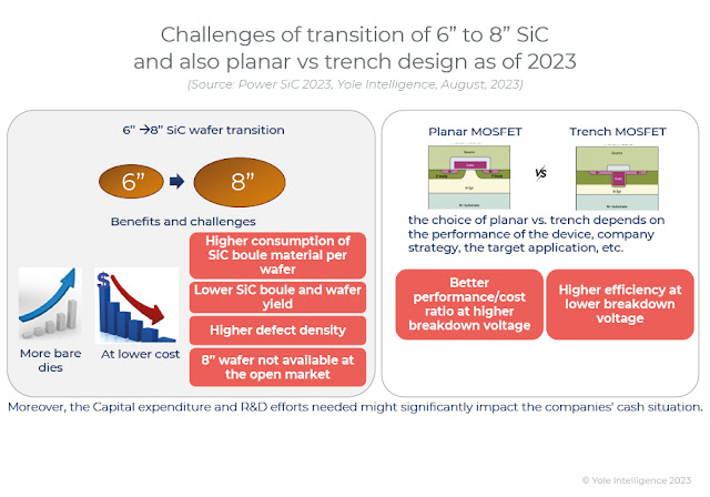
Strategic Shift to 8-Inch Wafers: Opportunities and Challenges Shape SiC's Next Phase
According to Yole, the Silicon Carbide (SiC) market is on a robust trajectory, poised to reach nearly $9 billion by 2028, driven by a dynamic blend of growth factors. The automotive sector, particularly Battery Electric Vehicles (BEVs) and 800V EV systems, spearheads this expansion. SiC's prominence extends to EV DC chargers, offering immense potential for high-power modular chargers. Additionally, SiC plays a pivotal role in energy supply, with installations expected to surge between 2022 and 2028. Industrial power supplies, motor drives, and rail systems further diversify SiC's applications. This Yole report underscores SiC's prowess in high-efficiency power electronics across industries, shaping a transformative market landscape.
The report indicates that as of 2023, the mainstream SiC wafer size for leading players is still 6 inches. However, there are strategic discussions and plans surrounding the transition to 8-inch (200 mm) SiC wafers. While Wolfspeed is currently the only player producing SiC devices on the 8-inch platform, other companies have announced their intention to follow suit. The adoption of 8-inch wafers presents both opportunities and challenges.
Challenges associated with 8-inch wafer production include higher costs, longer equipment lead times, potentially lower initial yield rates due to the larger size, and concerns about the availability of these wafers. Wolfspeed's early adoption of 8-inch wafer production reflects their proactive stance in developing the technologies and processes required to overcome these challenges.
The transition to 8-inch wafers is an area of focus due to the potential advantages it offers, such as increased capacity and improved cost efficiency over time. However, the challenges mentioned earlier are critical factors that need to be addressed for a successful transition. Companies are investing in innovative approaches and strategies to ensure a smooth migration to the 8-inch platform, which has the potential to impact the SiC power devices market significantly in the coming years.
Yole Group - Follow the latest trend news in the Semiconductor Industry
Thursday, August 31, 2023
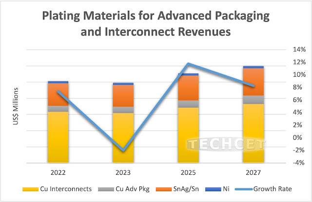
Metal Plating Chemicals Revenues to Boost into 2024
Growth driven by developments in leading-edge logic and memory
“Increased usage of advanced packaging, redistribution layers, and copper pillar structures are all factors contributing to the growth of the metal chemicals market segment,” states Dr. Karey Holland, Chief Strategist at TECHCET.
Balancing Fundamental and Applied ALD with Stacey Bent – ALD Stories Ep. 26
Wednesday, August 30, 2023
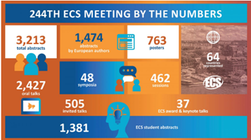
Announcement Symposium G01 on “ALD & ALE Applications, #19” at the 244th ECS Meeting in Gothenburg, Sweden, Oct. 8-12, 2023
Announcement Symposium G01 on “ALD
& ALE Applications, #19”
at the 244th ECS
Meeting in Gothenburg, Sweden, Oct. 8-12, 2023
See for detailed information about the 48 symposia, late manuscript submission requirements, and financial assistance: https://www.electrochem.org/244/.
6K Energy Partners with Forge Nano to Revolutionize Battery Material Production
6K Energy, a trailblazer in sustainable battery material production, has joined forces with Forge Nano to introduce cutting-edge Atomic Layer Deposition (ALD) technology for commercial-scale production of NMC 811 cathodes. This collaboration aims to transform the battery industry by enhancing performance, efficiency, and cost-effectiveness.
Forge Nano, known for its precision nano-coating technology, and 6K Energy are set to redefine battery material production. By integrating Forge Nano's proprietary Atomic Armor™ surface technology into 6K Energy's process, the partnership promises unparalleled advancements.
Atomic Armor employs ALD coatings with unprecedented precision and speed. This method enhances battery materials, resulting in superior capacity, safety, charging rates, and cost-efficiency. Combining Forge Nano's Atomic Armor with 6K Energy's innovative UniMelt® materials production process is expected to yield high-performance and cost-effective battery materials.
Dr. Richard Holman, Senior VP of Battery Products at 6K Energy, emphasizes the impact of the collaboration, stating, "Leveraging Forge Nano's Atomic Armor platform provides us with a coating technology that meets the stringent specifications of our lithium-ion battery materials."
6K Energy's mission to produce domestically sourced battery materials for electric vehicles and renewable energy is greatly amplified by this collaboration. As the demand for advanced battery technologies grows, strategic partnerships like this one are poised to drive sustainable and high-performance solutions.
About 6K:
6K is a sustainability-driven company offering innovative solutions across industries. Their UniMelt® microwave plasma production system transforms materials into groundbreaking products. The company's 6,000-degree philosophy signifies both the operational temperature of UniMelt and the sun's surface temperature. 6K Energy, a division focused on domestically sourced battery materials, accelerates the transition to electric vehicles and renewable energy.
For more information, visit www.6Kinc.com.
6K Energy to Implement Forge Nano Equipment for Commercial Production of NMC 811 - Forge Nano
Monday, August 28, 2023
The Future of Nanoimprint Lithography: Exploring Possibilities and Challenges for High-Volume Production
Nanoimprint lithography (NIL) has emerged as a promising technique for the replication of intricate nano-scale features, offering higher resolution and uniformity compared to traditional photolithography methods. As semiconductor technology advances towards smaller and more complex structures, NIL holds the potential to revolutionize high-volume production processes. In this blog post, we'll delve into the current status of nanoimprint lithography and the possibilities it presents for future high-volume productions, as well as the main issues and concerns that need to be addressed.
NIL utilizes a process where a patterned mask is brought into contact with a resist-coated substrate. The resist fills the relief patterns in the mask through capillary action, creating precise nano-scale features. With a focus on simplicity and cost-effectiveness, NIL doesn't require the complex optics found in traditional photolithography, making it an attractive option for semiconductor memory applications.
Early work on combining NIL and Atomic Layer Etching by AlixLabs Founders
Most Recent Achievements:
Recent study by TEL and Canon have demonstrated NIL's resolution capabilities of better than 10 nm, positioning the technology as a candidate for printing multiple generations of critical memory levels using a single mask. The potential to eliminate material waste by applying resist only where necessary adds to its appeal. Moreover, the simplicity and compactness of NIL equipment allow for clustered setups, enhancing productivity.
NIL Addressing Challenges in DRAM Scaling:
Dynamic Random Access Memory (DRAM) memory faces the challenge of continued scaling, with roadmap targets aiming at half pitches of 14 nm and beyond. The complexities of achieving tighter overlays, greater precision in critical dimensions, and edge placement errors demand innovative solutions. In DRAM fabrication, overlay requirements are even more stringent than in NAND Flash, with an error budget of 15-20% of the minimum half pitch.
Edge Placement Error (EPE):
EPE, the difference between intended and printed features, poses a significant challenge in modern semiconductor manufacturing. The intricacies of multiple patterning schemes and intricate device layouts contribute to EPE's complexity. Ensuring accurate placement of features is critical for maintaining device yield and performance.
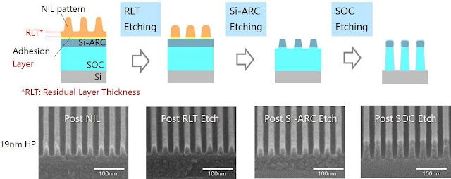
The Quasi-Atomic Layer Etch (Quasi-ALE) process
The process is a specialized etching technique employed in advanced semiconductor manufacturing, particularly in processes like Nanoimprint Lithography (NIL). Quasi-ALE combines elements of Atomic Layer Etching (ALE) and conventional etching methods to achieve precise and controlled material removal. In the context of Nanoimprint Lithography, Quasi-ALE is used to etch materials with exceptional precision, targeting nanoscale features while minimizing damage to the surrounding areas. It involves a cyclic process where alternating etching and passivation steps are applied to the substrate. Each cycle removes a controlled layer of material, ensuring highly uniform etching and minimal lateral etch. One can discribe Quasi-ALE as a more productive way of performing ALE.
The key steps of the Quasi-ALE process typically involve:
1. Etch Step: During this step, a reactive gas is introduced into the etch chamber, which chemically reacts with the material to be removed. This reaction results in the selective removal of the material layer.
2. Passivation Step: In this step, a passivating species is introduced, forming a protective layer on the substrate surface. This layer prevents further etching and preserves the material beneath.
3. Purge and Repeat: The chamber is purged to remove any excess gases, and the process is repeated in a cyclical manner. Each cycle removes a controlled atomic layer of material.
Quasi-ALE is particularly advantageous for applications requiring high precision and control, such as in Nanoimprint Lithography, where maintaining accurate pattern dimensions and minimizing damage is critical. By combining the benefits of both ALE and traditional etching, Quasi-ALE enables advanced semiconductor manufacturing processes to achieve unprecedented levels of accuracy and uniformity.
Addressing EPE with Nanoimprint Lithography:
Researchers are actively exploring techniques to mitigate edge placement errors in nanoimprint lithography. This includes focusing on overlay accuracy, critical dimension uniformity (CDU), and local CDU. Compensatory methods such as dose control and reverse tone pattern transfer are being investigated to improve CDU and minimize errors.
The Role of Dose Control:
Varying the exposure dose offers a means of achieving small shifts in critical dimensions. Initial studies suggest that dose variations could lead to CD shifts of one to 2 nm. This strategy holds promise for enhancing CDU in the imprint process.
Reverse Tone Pattern Transfer:
Reverse tone processes, involving spin-on hard mask (SOHM) application and etch-back, offer an alternative approach to pattern transfer. While this method provides advantages such as reduced resist erosion and improved wall angles, trade-offs between CDU and line width roughness (LWR) need to be addressed.
Looking Ahead: The Possibilities and Challenges:
While NIL exhibits impressive potential, there are key challenges to overcome before it can be effectively integrated into high-volume semiconductor manufacturing. Ensuring precise overlay accuracy, managing complex CDU requirements, and effectively addressing edge placement errors remain pivotal. As the industry strives to achieve the roadmap's aggressive scaling targets, the evolution of nanoimprint lithography will undoubtedly play a crucial role.
Nanoimprint lithography is poised to reshape the semiconductor manufacturing landscape, offering higher resolution and cost-efficiency compared to traditional methods. With ongoing research and development, addressing challenges such as overlay accuracy, CDU, and EPE, the path to successful high-volume production through NIL seems promising. As technology continues to advance, the journey towards perfecting nanoimprint lithography is an exciting one, holding the potential to shape the future of chip fabrication.
Tokyo Electron (TEL):
TEL specializes in Nanoimprint Lithography (NIL) technology, offering precision equipment, advanced etching solutions, and expertise in process control. They excel in alignment, overlay correction, CDU management, and etching technology.
Canon:
Canon contributes to Nanoimprint Lithography (NIL) advancement by leveraging TEL's strengths in alignment, overlay correction, CDU management, and advanced etching solutions. They integrate these capabilities with the Reverse Tone Pattern Transfer, ensuring precise pattern replication and fidelity. Canon's focus on innovation drives high-resolution, cost-effective solutions for semiconductor manufacturing.
Canon has introduced a groundbreaking solution in the field of semiconductor technology with the development of the world's first mass-production equipment called the "FPA-1200NZ2C." This innovative tool utilizes nanoimprint lithography, a cutting-edge technique that involves imprinting nanometer-scale mask patterns onto substrates. By adopting this novel approach, Canon aims to overcome the limitations of conventional miniaturization methods. The FPA-1200NZ2C is already in use by Toshiba Memory, a prominent semiconductor memory manufacturer. This advancement marks a significant step forward in semiconductor manufacturing, enabling the creation of more intricate and advanced circuit patterns.
Sources:
High-Definition Nanoimprint Stamp Fabrication by Atomic Layer Etching — Lund University
Nanoimprint post processing techniques to address edge placement error (spiedigitallibrary.org)
Nanoimprint Lithography | Canon Global
FPD Lithography Equipment | Canon Global
Benefits of atomic-level processing by quasi-ALE and ALD technique - IOPscience
Acknowledgement :
Thanks for sharing the SPIE article on LinkedIn and giving insights Frederick Chen!
Sunday, August 27, 2023
The Industiral Ecosystem of Si Chips and Atomic Layer Deposition - Webinar
 https://brnw.ch/21wC0I4


%20(1).png)


