Thursday, February 17, 2022

RASIRC Provide Record Low Resistivity Titanium Nitride Film Fabricated by Thermal ALD

Ultra-dry hydrazine enables growth at low temperature

San Diego, Calif – January 18, 2022 – An IITC paper authored by researchers from UCSD, Samsung, and RASIRC demonstrated record low resistivities for low temperature titanium nitride (TiN) films grown by thermal ALD process. Films yielded resistivities below 200 µohm-cm. The process used titanium tetrachloride (TiCl4) and ultra-dry anhydrous hydrazine along with surface treatments to further reduce surface impurities. The reduction of moisture was key. This reduction was achieved by a high vacuum ALD process combined with anhydrous hydrazine with moisture below 100ppb.

Low resistivity is an indicator of a high-quality film that works well as a barrier layer or conductor. TiN thin films are used as diffusion barriers for cobalt (Co) and tungsten (W) metal layers as well as gate metal in CMOS devices due to their high electrical conductivity and related low resistivity.

Historically, TiN films have been fabricated with ammonia and plasma. However, new three-dimensional designs with high aspect ratios (HAR) impose severe process limitations on plasma efficacy due to line-of-sight issues. Thermal ALD processes have a non-directional advantage over plasma if the process chemistry is reactive enough.

By replacing ammonia with hydrazine, reactivity is increased in the ALD process. This enables processing at lower temperatures needed for backend processes. Low temperature ALD is needed to avoid degradation of previously deposited structures. These breakthroughs make it possible for new 3D architectures like nanoribbons and nanotubes to move into high volume manufacturing.

“Once a low water background can be achieved in the tool, it is critical that the hydrazine precursor be as dry as possible to prevent oxygen incorporation in the film,” said RASIRC Founder and CEO Jeffrey Spiegelman. “Through proper tool design and ultra-dry BRUTE® Hydrazine, high quality titanium nitride films can be grown, as shown in the research.”

Details on the research were published in IEEE Xplore following the 2021 IEEE International Interconnect Technology Conference (IITC). For more information, contact RASIRC.
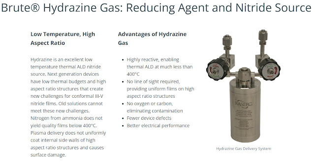

BRUTE Hydrazine

BRUTE Hydrazine enables uniform nitride deposition for titanium and early transition metals at low temperature. BRUTE Hydrazine may also be used as an atomic hydrogen source, where metals such as Ru, Cu, and Co may be cleaned and reduced. Brute Hydrazine has been formulated with a higher flash point for safer handling.

About RASIRC

RASIRC transforms liquids into dynamic gases that power process innovation in semiconductor and adjacent markets. By commercializing molecules for lower temperature processes, RASIRC patented technology enables the manufacture of atomic-scale oxides, nitrides, and metals. Innovative products such as BRUTE Peroxide, Brute Hydrazine, the Peroxidizer®, and Rainmaker® Humidification Systems are being used to develop solutions for 5G, AI, IOT, and advanced automation.


What makes RASIRC a unique industry leader is our technical expertise and commitment to solving complex industry challenges for our customers. Our team of industry experts has a proven track record of being first to market by efficiently delivering state of the art technology that reduces cost, improves quality, and dramatically improves safety. With our customers at the forefront of all we do, we continue to research, develop, and design innovative products that purify and deliver ultra-pure gas from liquids for the semiconductor and related markets. Contact RASIRC to help solve your complex problems.


P: 858-259-1220, email info@rasirc.om or visit http://www.rasirc.com


Thursday, February 10, 2022

ALD for Industry 2022, 29-30 March 2022 in Dresden

The 5th „ALD FOR INDUSTRY“ workshop will again show the bridge between basic science, industrialisation and commercialisation of this technology. According to a research study, „The global Atomic Layer Deposition Equipment (ALD) market is expected to reach USD 8.2 billion by 2026, growing at a CAGR of 28% from 2020 to 2026 layer, excellent adhesion of high aspect ratio surfaces and pinhole-free coatings.“


Interest in industrial solutions for Atomic Layer Deposition is increasing. This opens up new possibilities for innovative materials and designs in a wide range of applications. ALD is one of the best deposition methods for producing conformal and thin films. Furthermore, it is a key technology for the semiconductor industry, but not only for the semiconductor industry. Atomic layer deposition, is a thin film technology that enables new and highly innovative products for a wide range of applications.

In 2022 the EFDS will organize the 5th workshop „ALD FOR INDUSTRY“ in Dresden (Germany), at one of the focal points of European thin-film technologies in industrial applications and research. „ALD for industry provides the opportunity to get in touch with industrial and academic partners, to learn more about fundamentals of ALD technology and get informed about the latest research results on this topic.

The Workshop will focus on the currents markets for ALD and address the applications in Semiconductor industry, MEMS &Sensors, Battery technology, Medical, Display, Lightning and Photovoltaics.

EXHIBITION

You have the right products and services for our community? Come to the event and present your expertise.
At the exhibition you will have a table and space for one roll-up. During all breaks you will have the opportunity to get in discussion with the participants and speakers.

If you are interested, please contact info@efds.org with the comment „ALD for Industry“.

PROGRAM


Thank you to all speakers and the Program Committee. The Program for our Workshop 2022 is prepared. For more details please open the link above.

Program Committee 2022
Quentin Demarly, Air Liquide Advanced Materials, Paris, France
Dr. Christoph Hossbach, Picosun Oy and Picosun Europe GmbH, Dresden, Germany
Dr. Martin Knaut, IHM, TU Dresden, Germany
Prof. Mikko Ritala, University of Helsinki, Helsinki, Finland
Dr. Jonas Sundqvist, BALD Engineering AB, Wärmdö, Sweden
Dr. Claudia Wiemer, CNR IMM, Unit of Agrate Brianza, Italy

HOTEL RECOMMENDATION

114 EUR single room, including breakfast
Canceling free of charge until 7 days before the event
Code: ALD

Tuesday, February 8, 2022

Samsung Electronics Is Pushing Hard to Bring Monolithic 3D DRAM to HVM by 2025

Samsung Electronics has been enjoying its DRAM market leader position for about 30 years now. To retain the position further, it has intensified its R&D of monolithic 3D DRAMs to bring them to HVM by 2025.


DRAM’s performance boost based on scaling the cell size or pitch is approaching a physical limit for cramming more cells in a limited space. Additionally, the ultra-high aspect ratio capacitors may collapse leading to compromised device reliability. Therefore, switching from current 2D DRAMs to next-generation monolithic 3D DRAMs seems inevitable.

Samsung has reportedly intensified its R&D on stacking DRAM cells on top of each other in a monolithic fashion, unlike in the case of high-bandwidth memory (HBM), wherein multiple dies are stacked atop each other.

Besides High-k/Metal Gate transistor technology, Samsung is also considering adopting FinFET or gate-all-around (GAA) technology for the DRAM cell transistor to attain better electrostatic control of the charge flow within the channel with the gate electrode.

Micron Technology and SK Hynix are also reportedly developing monolithic 3D DRAMs. Micron recently filed a patent for a monolithic 3D DRAM that is different from that of Samsung. Micron’s approach is to change the shapes of the transistor and capacitor without laying down a cell. Major equipment manufacturers such as Applied Materials and Lam Research are also developing solutions for the monolithic 3D DRAMs.

By Abhishek Kumar Thakur & Jonas Sundqvist

Monday, February 7, 2022

Picosun and Shincron join forces for ALD optical coating development

ESPOO, Finland, 3rd of February 2022 – Picosun Group and Shincron Co., Ltd. have joined forces for development and commercialization of Atomic Layer Deposition (ALD) for optical coatings. ALD technology provides uniform and conformal coatings to the even most challenging structures and is therefore well suited for high-end optical applications.

The R&D teams from both companies have worked together to tailor existing ALD processes optimizing them for the use in optical applications. In addition to standard ALD optical films, ALD magnesium fluoride (MgF2) has been researched and is now available for commercial use for the first time. So far, ALD MgF2 processes have been only presented in academic research by universities and science institutes. MgF2 is a desired material in optical applications due to its low refractive index at visible light and high transmittance in FUV optical region. It can be used as a single layer or as part of an optical stack combining low and high refractive index materials. It has also other features, such as barrier properties and high chemical stability, which bring big advantages in some applications.


The collaboration agreement was first signed in 2019 including the appointment of Shincron as Picosun’s sales representative and ALD product distributor in Japan. The collaboration was extended with Joint Development Agreement (JDA) in 2020 with the aim to develop novel and advanced ALD coatings for optical applications.

“We are very excited about the collaboration. The teamwork has been fruitful, and the results obtained now are excellent. We see optical coatings as one of the emerging ALD applications and believe in strong growth in this market”, says Jussi Rautee, CEO of Picosun.

“We are happy to add ALD technology to our offering. This way we can increase our services for our customers. We have set up a demo capability for ALD optical coatings and Japanese optical companies have shown high interest for this process”, says Masaya Narita, CEO of Shincron.

Abstract submission - Atomic Layer Processing Modelling Workshop 15-16 March Sweden

The abstract submission and registration for our Atomic Layer Processing Modelling Workshop 15-16 March is now open at the conference website 2022 Atomic Layer Processing Modelling Workshop - Linköping University (liu.se) 

Join us in Linköping if the pandemic allows and/or online to discuss how to model atomic layer processes. No registration fee!


AtomicLimits: Atomic Layer Etch Carves the Path to More Efficient Computing

Here is a good blog post by Intermolecular at atomic Limits on advances in ALE and future prospects
  • High-volume manufacturing (HVM) of atomic-scale semiconductor devices requires new approaches to deposit and etch materials in complex nano-architectures. Next-generation logic devices, including gate all-around (GAA) transistors and the conductors that link them together, must be engineered with atomic precision.
  • The selective removal of materials also enables efficient integration schemes which mitigate costly lithography issues and could lead to new ways to make memory devices. Thermal atomic layer etching (ALE) of metals, dielectrics, and semiconductors provides atomically precise isotropic etching in 3D device structures. 
  • ALE processes must be selective to the materials to be etched, have robust process parameter windows, and leave minimal residues or surface damage. The complexity of experimental design requires close collaboration between chemists, process & integration engineers, and device designers, as well as new methods for combinatorial etch testing and smart data handling.
  • Meeting these requirements will ensure high device yields, a necessary outcome for success in the extremely competitive semiconductor market.


Examples of ALE of a trench structure, with poor kinetic control of the ALE process leading to inconsistent etch (top), or good control of the ALE process leading to a surface-limited reaction and consistent etching at high aspect ratio (bottom). (Source: Intermolecular, AtomicLimits.com)

Thursday, January 27, 2022

ALD InGaN with single precursor pulse of In & Ga

Polla Rouf of Pedersen Group in Linköping Sweden, just published an ALD approach to metastable In1−xGaxN with 0.1 < x < 0.5 based on solid In- and Ga-precursors that were co-sublimed into the deposition chamber in one pulse. A near In0.5Ga0.5N film with a bandgap value of 1.94 eV was achieved on a Si(100) substrate. Epitaxial In1−xGaxN(0002) was successfully grown directly on the 4H–SiC(0001) substrate.

I checked in with Prof. Pedersen on Twitter and this is gonna be one of the abstract submitted to AVS ALD 2022 in Ghent this summer.

  • The sequential pulsing of the precursors in ALD presents a challenge to depositing a homogeneous ternary material as only one precursor can be pulsed into the reactor at a time.
  • Ternary materials are therefore deposited by ALD as stacks of two binary materials. In1−xGaxN could therefore be deposited as layers of InN and GaN in an ABAB⋯CBCB… super-cycle approach where A and C are In- and Ga-precursors, respectively, and B is the N-reactant. By varying the number of cycles for each binary material, the overall composition of the ternary material can be tuned. 
  • This approach relies on diffusion of the two binary materials to form a homogeneous ternary phase. Otherwise, a multilayer of InN/GaN is obtained. This ALD approach has been used to obtain In1−xGaxN with x ranging from 0.15–0.85 using trimethylindium and trimethylgallium.
  • Here, an alternative method to depositing ternary materials by introducing both metal precursors with a single pulse. This renders mixing of the metals in both the growth direction and in the growth plane. This was achieved by mixing and co-subliming two solid metal precursors into the ALD chamber.


Wednesday, January 26, 2022

AVS Seminar Atomic Layer Deposition from an Applications Perspective by Prof. Kessels

 Coming up soon - AVS Seminar Atomic Layer Deposition from an Applications Perspective by Prof. Kessels, TU Eindhoven.

Read about the background at AtomicLimits LINK.

Atomic Layer Deposition from an Applications Perspective

February 9, 2022
1:00 PM - 5:00 PM
Instructor(s): Erwin Kessels
REGISTER HERE!

Questions? Contact Heather Korff, heather@avs.org, 530-896-0477


Cover image - ALD Applications from AtomicLimits.com. Schematic overview of the (emerging) industrial applications of atomic layer deposition (ALD). Roughly speaking three main areas can be distinguished: those related to (opto)electronic integrated circuits (blue); those related to large area electronics and energy technologies (red) and other applications (green) that are often in niche markets. The layout of the figure is inspired by a figure posted on the Strem Chemicals website (by BALD Engineering AB). A high-resolution version of this figure can be found in the AtomicLimits Image Library.


Monday, January 24, 2022

BENEQ gives insights to the growing USD 345 Million More than Moore market for ALD Equipment

Here is an insightful interview with Patrick Rabinzohn, Ph.D., VP of the Semiconductor ALD Business Unit at Beneq regarding ALD in the More than Moore market (MtM) LINK. Yole Development recently release a report on the topic as summarized below.

Atomic Layer Deposition (ALD) is known in the electronics industry as an enabler for the scaling of logic and memory semiconductor devices. Ultimately, this scaling leads to performance improvement of devices such as dynamic random-access memory (DRAM), advanced fin field effect transistor (FinFET) and Gate All Around transistors. ALD is now percolating into More-than-Moore (MtM) device production, again enabling novel architectures, materials, and performance improvements. Examples include GaN and SiC transistors, in particular GaN High Electron Mobility Transistors (HEMTs) and SiC trench metal oxide semiconductor FETs (MOSFETs), piezoelectric microelectromechanical systems (MEMS) and radiofrequency (RF) devices or compound semiconductor mini-light emitting diodes (LEDs) and micro-LEDs.

Besides the technical benefits that ALD offers, surging ALD equipment sales are propelled by fab capacity expansions worldwide. Forecasts expect the ALD equipment market for MtM devices to grow in the coming years with a 12% Compound Annual Growth Rate from 2020-2026 (CAGR2020-2026) reaching $680.5M in 2026.
You can find detailed know-how, market, and ecosystem overview of ALD equipment dedicated to MtM device production in the technology and market report Atomic Layer Deposition Equipment for More than Moore 2021, published by Yole Développement (Yole). Among the featured equipment manufacturers, Beneq is gaining momentum in the MtM space with a rapidly growing equipment lineup.

Picosun part of extensive quantum technology 10 Million Euro QuTI project is coordinated by VTT Technical Research Centre of Finland

ESPOO, Finland, 18th of January 2022 – Picosun takes part as an industrial partner in QuTI, a recently launched extensive research project aiming to develop new components, manufacturing and testing solutions that are needed in quantum technology. Quantum technology has gained interest in a vast array of industries on a large scale. The remarkable performance improvements it offers enable for example powerful computing and benefits in communications, healthcare, sensors, imaging and measurement applications.


The QuTI project is coordinated by VTT Technical Research Centre of Finland, and it has a total budget of around 10 million euros. Other industrial partners of the consortium include Bluefors, Afore, IQM, Rockley Photonics, CSC, Quantastica, Saab and Vexlum. The research partners are VTT, Aalto University and the University of Tampere.

“Quantum technology is a multidisciplinary and rapidly advancing field. The QuTI consortium provides an ideal starting point for strengthening the international competitiveness of Finnish technology and industry in this fast-growing field,” says QuTI project’s coordinator, Research Professor Mika Prunnila from VTT.

“Quantum technology has already taken the step from research laboratories to commercial applications. We look forward in supporting this development trend even further and being part of creating a globally competitive industrial ecosystem in Finland around this technology,” says Dr. Jani Kivioja, CTO of Picosun Group.

“Atomic Layer Deposition, or ALD, is the advanced thin film coating method for ultra-thin, highly uniform and conformal material layers that enables the digital solutions of today. It will also play a crucial role in future innovations and in the quantum computing, communication and sensing devices that will be developed in the QuTI project”, continues Jussi Rautee, CEO of Picosun Group.


More information:
Jani Kivioja
CTO, Picosun Group
Tel: +358 46 922 8804
Email: info@picosun.com

Picosun provides the most advanced ALD (Atomic Layer Deposition) thin film coating solutions for global industries. Picosun’s ALD solutions enable technological leap into the future, with turn-key production processes and unmatched, pioneering expertise in the field – dating back to the invention of the technology itself. Today, PICOSUN® ALD equipment are in daily manufacturing use in numerous leading industries around the world. Picosun is based in Finland, with subsidiaries in Germany, USA, Singapore, Japan, South Korea, China mainland and Taiwan, offices in India and France, and a world-wide sales and support network. Visit www.picosun.com.


Friday, January 7, 2022

TSMC Self-Aligned Via Process Development for Beyond the 3nm Node

Semiwiki Tom Dillinger reports on an interesting paper by TSMC at the recent IEDM 2021 conference in San Francisco using selective ALD with the help of SAMs or Dielectric on Dielectric (DOD) as it is called.


From the article sumary: Continued interconnect scaling below the 3nm node will necessitate unique process development research to maintain electrical and reliability specs in the presence of (up to 4nm) overlay error. The need for low-K interlevel dielectrics is a given – yet, the via etch in these materials is not especially tolerant of EPE.

TSMC has demonstrated a potential process flow for a “self-aligned via” with an additional DoD material. The etch rate differential of the DoD results in more robust via-to-adjacent metal reliability. This process flow utilizes two unique steps – the SAM of a blocking material on metal surfaces, and the selective ALD of a dielectric-on-dielectric.

Thursday, December 30, 2021

Interview with Maksym Plakhotnyuk, CEO & Co-Founder, Atlanta 3D Nanosystems

Here an insightful interview with Maksym Plakhotnyuk, CEO & Co-Founder, Atlanta 3D Nanosystems on Advancements in Micro & Nano Electronics – What it Means for the Semiconductor Industry

ATLANT 3D Nanosystems is a cross-European deep tech company that developed a unique atomic layer advanced manufacturing technology (direct write ALD) with a mission to reshape the future atom by atom and enable on-demand advanced materials development, rapid prototyping and manufacturing of microdevices and nanodevices. ATLANT 3D team is highly dynamic, international, and multidisciplinary, consisting of 15 experienced entrepreneurs, engineers and scientists. ATLANT 3D collaborates with leading European universities, such as SAS, DTU, FAU, TNO, SUPSI and industrial partners such as Merck, ST Microelectronics, Prima Industrie and SEMPA.


Wednesday, December 15, 2021

Redstone’s North Karelia Growth Fund makes a pre-seed investment in Chipmetrics, a spin-off of VTT Finland

Redstone’s North Karelia Growth Fund makes a pre-seed investment in Chipmetrics, a spin-off of VTT. Chipmetrics is based in Joensuu, Finland, one of the leading photonics hubs in Europe. The company is a forerunner in productizing test structures, test chips, and related measurement concepts for advanced materials and microelectronics manufacturing industries.

The 3D nanometrology startup is part of the emerging Atomic Layer Deposition industry and research community. ALD is a key enabler of the 3D megatrend in the semiconductor industry by improving the performance and energy efficiency of transistors and memory circuits.

We wish CEO Mikko Utriainen and the whole team the best of success in this sizable global industry and are delighted to support the venture.

Chipmetrics will launch a seed round in 2022. We are looking forward to seeing you grow!


Tuesday, December 14, 2021

2022 Atomic Layer Processing Modelling Workshop

Pedersen group is organizing a work shop on modelling of atomic layer processes in Linköping 15-16 March next year with a Tutorial by Ray Adomaitis. Possibility to join via Zoom. 


Welcome to a forum where experimentalists and modellers from academia and industry meet to collaboratively push the boundaries of multi-scale modelling.

Predict the Future of Thin Films

Is complete in silico development of new materials and methods a utopia or just around the corner? Join us on-site or online and discuss state-of-the-art scientific methods to model atomic layer processes such as CVD, ALD and ALE, from reactorscale to atomic level.

The conference will have a mix of contributed talks, describing the latest in ALP modelling (atomic layer processing) and industry lectures presenting areas that need modelling. 

Tutorial

Prof. Raymond Adomaitis, from University of Maryland, will describe his way of modelling ALP in the tutorial “Reaction network analysis of ALD processes: Is this a true ALD cycle? What rates can be measured?”.


Date and time: March 15-16, starting on Tuesday at 12.00. 

Place: Planck, Fysikhuset. You will also be able to participate online via link.

Abstract deadline: February 2022.

The conference is free of charge but to participate you will have to register. Registration and Abstract aplication will soon be available here.


Wednesday, December 8, 2021

Meaglow Hollow Cathode Gas Plasma Source Paper Published by the Journal “Coatings”

Meaglow technical staff have published a paper entitled: “Recent Advances in Hollow Cathode Technology for Plasma-Enhanced ALD — Plasma Surface Modifications for Aluminum and Stainless-Steel Cathodes” in the journal “Coatings”. An early version of the paper can be accessed at the journal website, here.

The paper provides a brief review of oxygen contamination from ICP and microwave legacy sources, but also provides details of the operation of the hollow cathode gas plasma sources now widely used by the ALD community.


Tuesday, December 7, 2021

How Machine Learning Enables Accurate Prediction of Precursor Volatility

by Simon Elliott, Director of Atomic Level Process Simulation, Schrödinger

Challenges in predicting volatility

A crucial process in manufacturing CPUs and other high-tech devices is the deposition of solid material from reactive vapors. Different precursor vapors are used for chemical vapor deposition, vapor phase epitaxy, atomic layer deposition – and indeed the reverse process of atomic layer etching – with the precursor chemistry carefully designed for each case so as to control material quality at the nanoscale. But what all these techniques have in common is that the precursor chemicals must evaporate or sublime at a low enough temperature. Too much heating when vaporizing a precursor can make it decompose, causing it to be undeliverable to the growing surface.

With volatility playing such a central role in this technology (and in other fields like distillation, refrigeration, inkjet printing, food, and perfumes), it is surprising that we understand so little about it. Volatility is the product of a remarkably fine balance of interatomic forces, dictating the extent to which molecules condense together as a solid or liquid, or bounce apart into a vapor and deliver a certain vapor pressure at any given temperature. These interatomic forces can be computed very precisely with quantum mechanics for one molecule or a group of molecules, but not at the scale of a liquid or solid. Even with today’s computing power, routinely and accurately predicting precursor volatility ‘from first principles’ remains unfortunately out of reach.

Machine learning approaches

Could an alternative more empirical approach prove useful? Does enough experimental data exist to find the relation between volatility and chemical structure? The vaporization of some organic molecules, such as alcoholic fractions or natural fragrances, has been of interest for centuries and high-quality vapor pressure data are available in the literature. Over the last decade, these data have been analyzed with advanced fitting algorithms that come under the umbrella of ‘machine learning’. Schrödinger has leveraged the latest machine learning techniques to develop a highly accurate model that predicts the volatility of organic molecules up to C20.

However, when building machine learning models to predict volatility of precursor molecules, which are typically organometallic complexes, the situation is not so straightforward. New precursor molecules are constantly being proposed and evaluated. Commercial sensitivity sometimes means that data are partially withheld or plagued by experimental configuration differences from laboratory to laboratory. Additionally, for the common aim of material processing, complete pressure-temperature curves are rarely measured, as it is more pragmatic to focus on the temperature for vapor to transport successfully to the reactor. As a result, datasets for building predictive models are sparse and incomplete.

Prediction of volatility for inorganic and organometallic complexes 

Schrödinger scientists embarked on the challenge of building machine learning models to predict the volatility of precursor molecules. Using in-house expertise in machine learning and advanced informatics, Schrödinger scientists collated and digitized information about organometallic precursors from disparate literature sources and applied a variety of machine learning algorithms (such as Random Forest and Neural Networks) in conjunction with different chemoinformatic descriptors and fingerprints. The result is the first capability of its kind for accurately and efficiently predicting the volatility for inorganic and organometallic complexes from their chemical structures. For complexes of the fifty most common metals and semimetals, the model predicts the evaporation or sublimation temperature at a given vapor pressure with an average accuracy of ±9°C (which is about 3% of the absolute temperature). As a trained model, the turnaround time is fast with the ability to compute hundreds of complexes per second.

New avenues for precursor development

This predictive model opens a new path for designing novel precursors with improved performance, not only improving their deposition or etch chemistry, but also optimizing the temperature at which they evaporate or sublime and can be delivered as a vapor. This advance will allow a much wider range of structural modifications to be screened computationally than before and will produce candidate precursors for experimental synthesis and testing that are both less risky and more innovative. This volatility model, together with Schrödinger’s quantum mechanics-based workflows for computation of reactivity and decomposition, gives scientists a complete design kit for vapor-phase deposition or etch, delivering a faster pace of research into materials and processes for new technologies.

* The banner image is from Tyndall National Institute.

About the author


Dr. Simon Elliott is Director of Atomic Level Process Simulation at Schrödinger. From 2001-2018 he led a research group at Tyndall National Institute, Ireland. Prior to that, he studied chemistry at Trinity College Dublin and Karlsruhe Institute of Technology. He qualified as a Project Management Professional and is a Fellow of the Royal Society of Chemistry. He was co-chair of the 16th International Conference on Atomic Layer Deposition and chair of a 175-member COST network on the same topic.

About Schrödinger

Schrödinger is an industry-leading computational solutions provider for both life science and materials science, with a mission to improve human health and quality of life by transforming the way therapeutics and materials are discovered.

With the goal to accelerate the discovery and optimization of novel materials by a digital chemistry platform governed by physics-based modeling, amplified by machine learning, and optimized through team-based intelligence, Schrödinger’s Materials Science platform offers unprecedented insights into the mechanisms and properties of materials and chemical systems in a wide range of technological applications: Organic Electronics, Polymeric Materials, Consumer Packaged Goods, Catalysis & Reactive Systems, Semiconductors, Energy Capture & Storage, Complex Formulations, Metals, Alloys & Ceramics.

Learn more

Request more information


Beneq unveils two new ALD products for 300mm and compound semiconductor device fabrication respectively

Beneq revolutionized ALD cluster tools for More-than-Moore device makers with the highly successful Beneq Transform® family of products. Today, Beneq broadens its product portfolio further with two new distinct solutions: the Transform® 300 and ProdigyTM.

The Beneq Transform 300 and Prodigy were each created in response to specific technology requirements in the semiconductor manufacturing sector.

“The Transform 300 is designed to meet the growing demand of emerging semiconductor applications at 300 mm for devices such as CMOS image sensors, Power Devices, Micro-OLED/LED, and Advanced Packaging, which call for a high degree of versatility,” explains Patrick Rabinzohn, Vice President, Semiconductor ALD at Beneq.

“We created Prodigy to address those market segments that need a simple solution supported by high-end technology. It inherits the ALD design and processing knowhow we at Beneq have developed over the last 15 years, packing advanced features in a simpler, targeted industrial form factor,” continues Rabinzohn.
Beneq Transform 300 is the only 300 mm ALD cluster tool that combines thermal ALD (batch) and plasma ALD (single wafer) technologies to provide a highly versatile platform for IDMs and foundries. It is dedicated to advanced thin-film applications in CIS, Power, Micro-OLED/LED, Advanced Packaging and other MtM applications.

Beneq Tranform 300 is a highly configurable platform that caters to multiple advanced thin-film applications ranging from gate dielectric including in high aspect ratio trenches, to anti-reflection coating, final passivation or encapsulation, Chip-Scale-Packaging and beyond.

Beneq Prodigy is the deal manufacturing solution for compound semiconductor including RF IC’s (GaAs/GaN/InP), LED, VCSEL, Light Detectors and for MEMS manufacturers and foundries looking to enhance device performance and reliability through an affordable stand-alone ALD batch tool. Beneq Prodigy provides best-of-breed passivation and encapsulation films across multiple wafer types and sizes.

To learn more, visit:


Thursday, December 2, 2021

Master Program in ALD at Helsinki University!

On de­mand tailored train­ing  

We can organise special training on ALD and thin film characterisation. The content can be specifically tailored to meet your specific needs. Contact for further details!
M.Sc. in ALD

Application period for our Master's programme is open! Apply now to study inorganic materials chemistry with a focus on atomic layer deposition.

HelsinkiALD / ALD center Finland is now providing a well thought-out academic education program on Atomic Layer Deposition with skills highly relevant for also other thin film technologies.

The selected students will be majoring from Inorganic materials chemistry study track of Master’s Programme in Materials Research (link), but the courses are directed so that they are covering all important aspects of ALD, including precursors, thin film deposition and characterization as well as potential applications.

As a final part, Master's Thesis in the field of ALD is carried out, either in our HelsinkiALD team or companies working on ALD technology. Upon graduation a special certificate on the ALD focus will be awarded together with the Inorganic materials chemistry diploma.

List of courses for ALD master studies. Optional course selection agreed with the supervisor, with strongest recommendation to courses listed below.


Wednesday, December 1, 2021

Webinar RIE and ALE Processes for Quantum Devices

Optimise the Fabrication Process for Quantum Devices, 2nd December, 4 pm (GMT)

Dr Russ Renzas, Quantum Technology Market Manager

The fabrication of superconducting qubits, quantum photonic elements and diamond-based quantum sensors require highly controlled, stable processes that will not damage the surface and leave no residues. Plasma-based Reactive Ion Etch and Atomic Layer Etch processes are critical for the fabrication of these quantum devices.

In this webinar, Dr Russ Renzas will give an overview of the available plasma etch solutions and how each one of them can be used to overcome some of the processing roadblocks, providing specific examples of how they are applied during the fabrication process

This webinar will give an introduction of:
  • The various etch platforms that are available and their differences
  • How each etch system can be used to overcome some of the processing roadblocks
  • Quantum-specific examples of what can be done and why it should be done during device fabrication process


REGISTER NOW

Thursday, November 25, 2021

Watch again - Material development for MRAM and FRAM stacks at Fraunhofer IPMS-CNT

Material development for MRAM and FRAM stacks

Dr. Lukas Gerlich & Konrad Seidel (Fraunhofer IPMS - Center Nanoelectronic Technologies)

Today, data is the lifeblood disrupting many industries. The vast majority of this data is stored in the form of non-volatile magnetic bits in hard disk drives. This technology was developed more than half a century ago and has reached fundamental scaling limits that prevent further increases in storage capacity. New approaches are needed.

In the webinar, FRAM (Ferroelectric Random Access Memory) and MRAM (Magnetoresistive Random Access Memory) will be presented as two promising concepts for future ultra-low power memory technologies. Special attention will be paid to material development and fabrication on state-of-the-art industrial equipment for 300 mm wafers.


Previous Webinar: Fe- FET - A Memory Device for Maximum Integration, Konrad Seidel (IoT Components and Systems) Webinars - Fraunhofer IPMS


Tuesday, November 23, 2021

Picosun Group has launched an ALD Medical Materials Library

Picosun Group has launched a Medical Materials Library consisting of over ten materials intended for medical-related coating and encapsulation with ALD.


"Picosun’s Medical Materials Library targeted to the medical device manufacturer segment reflects the innovative spirit of the company. I’m really excited over the fact that we are able to flexibly design tailored encapsulations according to our customers’ needs. I’m especially proud of our medical customers and partners who are already in pre-clinical and clinical trials with their ALD coated devices”, says Juhani Taskinen, Vice President, Medical Business Area of Picosun Group.


The materials library is a reflection of over six years extensive research and development that shows ALD can render biocompatibility to a substrate coated with Picosun library materials. Biocompatibility tests were carried out according to ISO standards in accredited third-party laboratories. The performed tests included for example cytotoxicity, antimicrobial activity, skin irritation or sensitization, hemocompatibility, bacterial endotoxins, bioburden and sterilization residuals. From the tested materials Picosun is able to design tens of different types of end materials according to customer needs.

ALD technology provides dimensionless coating thus enabling miniaturization of components and devices in the field of electronic implants. Antibacterial function together with excellent barrier properties and outstanding corrosion resistance pave the way for using the materials both in electronic and orthopedic implants and show high potential in pharmaceutical packaging. The superior film uniformity and conformality ensure a pinhole-free coverage over even the smallest details of the device.


Friday, November 19, 2021

How Did Plasmas Change ALD? - w/ Erwin Kessels (ALD Stories Ep 8)

In Episode 8 of ALD Stories, Tyler chats with Eindhoven University of Technology professor, Erwin Kessels, about plasma-enhanced ALD, industry applications, and Erwin's Atomic Limits blog & teaching strategies. 

In this video: 
00:00 - Intro
  01:46 - PEALD Basics, Ions, & Applications 
20:56 - Semiconductor Industry Advantages 
28:05 - Photovoltaic Passivation 
36:43 - Atomic Limits Blog & Teaching 
45:25 - Outro 

Professor Erwin Kessels - https://www.tue.nl/en/research/resear... 
Atomic Limits Blog - https://www.atomiclimits.com/


Thursday, November 11, 2021

Call for abstracts - AVS 22nd International Conference on Atomic Layer Deposition (ALD 2022) in Ghent, Belgium


Call for Abstracts
Due February 3, 2022
The AVS 22nd International Conference on Atomic Layer Deposition (ALD 2022) featuring the 9th International Atomic Layer Etching Workshop (ALE 2022) will be a three-day meeting dedicated to the science and technology of atomic layer controlled deposition of thin films and now topics related to atomic layer etching. Since 2001, the ALD conference has been held alternately in the United States, Europe and Asia, allowing fruitful exchange of ideas, know-how and practices between scientists. This year, the ALD conference will again incorporate the Atomic Layer Etching 2022 Workshop (ALE 2022), so that attendees can interact freely. The conference will take place Sunday, June 26-Wednesday, June 29, 2022, at the International Convention Center (ICC) Ghent in Ghent, Belgium.

As in past conferences, the meeting will be preceded (Sunday, June 26) by one day of tutorials and a welcome reception. Sessions will take place (Monday-Wednesday, June 27-29) along with an industry tradeshow. All presentations will be audio-recorded and provided to attendees following the conference (posters will be included as PDFs). Anticipated attendance is 800+.
Key Deadlines:
Abstract Submission Deadline: February 3, 2022
Author Acceptance Notifications: March 16, 2022
Early Registration Deadline: May 15, 2022
Hotel Reservation Deadline: May 25, 2022
JVST Special Issue Deadline: November 1, 2022
ALD Program Chairs
 
Program Chair:
Christophe Detavernier
(Ghent University, Belgium)

Program Co-Chair:
Jolien Dendooven
(Ghent University, Belgium)

Program Co-Chair:
Paul Poodt
(TNO/Holst Center,
The Netherlands)
ALE Program Chairs

Program Chair:
Erwin Kessels
(Eindhoven University of Technology, The Netherlands)

Program Co-Chair:
Harm Knoops
(Oxford Instruments,
The Netherlands)

Program Co-Chair:
Jean-Francois de Marneffe
(imec, Belgium)

2021 November Networking - ALD at Aalto University

Date and time: Fri 26.11.2021 starting at 13 Event will be held at Aalto CHEM, Kemistintie 1, Espoo and online in Zoom at https://aalto.zoom.us/j/68826769819 (password to be sent to registered participants via email a few days before the event)


Programme consists of (1) lectures (can be followed in Zoom): 
Brief introduction to ALD, Invited guest talks (Prof. Barry, Prof. van Ommen, Prof. Malygin), update of the Virtual Project on the History of ALD (VPHA); and (2) posters by local ALD research (not in Zoom) ("local" may be broadly interpreted).

Registration DL for participation with posters: Sun 14.11.2021. The number of posters may need to be limited; "first come, first serve".

Registration DL for local in-person participation: Mon 22.11.2021. The number of participants may need to be limited; "first come, first serve".

Registration DL for Zoom participation: Wed 24.11.2021. The number of participants might need to be limited (but likely not); if limiting is needed, "first come, first serve".

Organizing committee: Prof. Riikka Puurunen (chairperson), Dr. Aitor Arandia Gutierrez, Dr. Jorge Velasco, M.Sc. Jihong Yim. All from Aalto University, School of Chemical Engineering, Department of Chemical and Metallurgical Engineering, Catalysis research group.


AlixLabs, Breaking through the Crisis – Startups

While the world is dealing with the semiconductor shortage, startups are gearing up to fill in the gap with their innovative offerings to ensure that crisis doesn’t last long. In this interview, the co-founder and CEO of AlixLabs, Dr. Jonas Sundqvist discusses about what led us to this crisis, how to fix it and what role startups have in ensuring interrupted supply of silicon. He also discusses about what next when this crisis is fixed? Is there another crisis that may arise?


Tuesday, November 9, 2021

NCD Supplied new ALD equipment for protective coating of semiconductor equipment’s products

NCD supplied new ALD equipment to the customer based in Korea for coating products used in semiconductor equipment to protect from corrosion and plasma arcing. The customer could expect longer part lifetime and lower operation expense through this special coating because of improving reliability of process and protecting parts from damages.

Productivity and cost competitiveness have been more and more important in semiconductor industry. Using special coating, the competitiveness could be much increased by protecting particle generation and damage of semiconductor production, and cost down by longer maintenance period.

Normally protective coating on parts is used thermal spray coating, anodizing process and sputtering but they have some limitation because it is difficult to coat uniformly on complicated and micro-shaped products by those methods. However ALD process could solve that problem.

Complex shaped shower heads and electro static chucks in the equipment using etching and dry cleaning process with corrosive gases as well as plasma, could be expected to apply ALD process. Because shower heads have a lot of fine holes and ESCs have wafer lift pin holes so those products couldn’t be coated uniformly by CVD and PVD methods. Therefore ALD might be very essential for special coating for these products.

ALD Al2O3 coating to protect part damage is used normally because Al2O3 process has already been confirmed in many application area. ALD Y2O3 will be studied actively for the next protective coating because it has much more anticorrosive property than ALD Al2O3.

This supplied equipment, Lucida GSH500, applied NCD’s creative high throughput and large area ALD technology could load multi semiconductor products at the same time and run uniform ALD coating. NCD will keep our best to develop the more competitive ALD technology and equipment to expand various new application fields in the future.


<Lucida GSH500>