Tuesday, April 19, 2016

Behold - Solmates PLD is the next disruptive deposition technology following ALD

Behold ALD people - After defeating both PVD and CVD numerous times there will be now rest for the PLD guys ar coming - Solmates’ PLD platform is the next disruptive deposition technology following the adoption of atomic layer deposition (ALD) for thin film manufacturing - Welcome to the club PLD people!


ENSCHEDE, the Netherlands, April 18th 2016- Solmates has received an important and high profile order for its Pulsed Laser Deposition (PLD) equipment from world–leading nanoelectronics research center imec.  The system is scheduled for delivery to imec in Leuven, Belgium during Q2 2016.

Solmates’ advanced PLD equipment is fundamental in helping to accelerate the entry of new processes into commercial products. It plays a key role in the development of future chip designs and the integration of new materials for next generation transistors.

Solmates will become a member of imec’s Industrial Affiliation Program (IIAP) Beyond CMOS. This program focuses on the integration and benchmarking of novel device concepts beyond traditional transistor scaling. These include piezoelectrics for alternative computing devices and 2D materials such as graphene and MoS2 for ultimate scaling.

“This important and significant deal fits our roadmap towards mainstream CMOS compatibility,” commented Solmates’ CEO Arjen Janssens, “Imec is a world-leading center for nanoelectronics with significant global partnerships and therefore represents the perfect gateway to this key market.”

Solmates’ PLD platform is the next disruptive deposition technology following the adoption of atomic layer deposition (ALD) for thin film manufacturing. The technology uses a laser to create a plasma of the material to be deposited, enabling industrial quality deposition of new generation materials. An automated tool offers high yield, customized deposition of various ‘More than Moore’ materials on a wide variety of different substrates. The technology is already in use at various customer sites and several processes are qualified for (Piezo) MEMS, LED and PowerIC applications. Solmates owns key patents related to PLD technology and processes.

Monday, April 18, 2016

ALD and CNT template produces sub-5 nm features

As reported by Nanotechweb.org : Researchers at Korea University are reporting on a new way to make nano-trenches less than 5 nm deep with a technique called atomic-layer deposition (ALD), and single-walled carbon nanotubes as templates. The structures produced could be used to make high-density resistive components for a wide range of nanoelectronics devices.

Full story here

(a) Schematic diagram representing the creation of SiO2 nano-trenches. AFM image of (b) nano-trenches after further reactive ion etch of SiO2 through an alumina mask, and (c) SiO2 nano-trenches obtained by an additional etching in RIE and wet etching of alumina. Courtesy: Nanotechnology

Sunday, April 17, 2016

Applied Materials on the challenges of bringing new ALD Precursors to production

Here is an excellent interview with Dr. David Thompson, Senior Director, Center of Excellence in Chemistry,  Applied Materials on the challenges of bringing new ALD Precursors to production. For those of you who still have the possibility there will be a opportunity to meet and talk to David Thompson at the CMC Conference 5-6th of May (see details below).

Controlling Variabilities When Integrating IC Fab Materials

By Ed Korczynski, Senior Technical Editor, SemiMD/Solid State Technology,
copyright ©2016 Extension Media

Semiconductor integrated circuit (IC) manufacturing has always relied upon the supply of critical materials from a global supply chain. Now that shrinks of IC feature sizes have begun to reach economic limits, future functionality improvements in ICs are increasingly derived from the use of new materials. The Critical Materials Conference 2016—to be held May 5-6 in Hillsboro, Oregon (cmcfabs.org)—will explore best practices in the integration of novel materials into manufacturing. Dr. David Thompson, Senior Director, Center of Excellence in Chemistry, Applied Materials will present on “Agony in New Material Introductions – minimizing and correlating variabilities,” which he was willing to discuss in advance with SemiMD.

The full interview by By Ed Korczynski, Senior Technical Editor, SemiMD/Solid State Technology and Co-CHair of The CMC Conferecne is published in SemiMD and can be found here: http://semimd.com/blog/2016/04/15/controlling-variabilities-when-integrating-ic-fab-materials/  

 Buy Reports  | CMC Fabs   |  CMC Conference  |  Register Now

New Additions to a Powerful Lineup 
May 5-6, Hillsboro, Oregon


The Critical Materials Conference provides a framework to catalyze the flow of actionable technical and supply chain information related to critical materials. 

New Additions to the Critical Materials Conference Include: 

  • David Thompson, Ph.D., Director of Process Chemistry of Applied Materials
    • Agony in New Material Introductions - Minimizing and Correlating Variabilities
  • Toshi "Tommy" Oga, Ph.D., Gigaphoton Inc.
    • Neon Efficiency Improvement/Recycling
  • Dan Alvarez, Ph.D., Chief Technology Officer - RASIRC
    • Hydrazine as a Low Temperature Nitride Source: Materials Challenges for High Volume Manufacturing

A highly differentiated program, with networking opportunities for all attendees. 
For full agenda details click here.

Conference themes center around the Critical Materials Council and global IC fabrication industry needs. While executive conferences typically focus on the "what" and "why" of materials technologies, this conference also discusses "how" new materials can be controllably, safely, and cost-effectively used in fabs. Additionally the Conference includes market data to validate "when" materials will be needed. Attendees from fabs, OEMs, and materials suppliers alike have the opportunity to interact with the presenters and colleagues, to gain insights into the best practices of the entire supply-chain.

For more information on the conference go to www.cmcfabs.org/seminars/ 
Great Sponsorship Opportunities available, 
please contact cmcinfo@techcet.com or call 1-480-382-8336


Sponsors and Committee


Tesla coil causes carbon nanotubes to self-assemble into long wire

This is a cool must watch video on self assembly of carbon nano tubes into long wires from researchers at Rice University. HOUSTON – (April 14, 2016) – Scientists at Rice University have discovered that the strong force field emitted by a Tesla coil causes carbon nanotubes to self-assemble into long wires, a phenomenon they call “Teslaphoresis.”

 The team led by Rice chemist Paul Cherukuri reported its results this week in ACS Nano. - See more at: http://news.rice.edu/2016/04/14/nanotubes-assemble-rice-introduces-teslaphoresis/#sthash.LeL6G50r.dpuf

Teslaphoresis of Carbon Nanotubes

Lindsey R. Bornhoeft, Aida C. Castillo, Preston R. Smalley, Carter Kittrell, Dustin K. James, Bruce E. Brinson, Thomas R. Rybolt, Bruce R. Johnson, Tonya K. Cherukuri, and Paul Cherukuri
 
ACS Nano, Article ASAP
 
This paper introduces Teslaphoresis, the directed motion and self-assembly of matter by a Tesla coil, and studies this electrokinetic phenomenon using single-walled carbon nanotubes (CNTs). Conventional directed self-assembly of matter using electric fields has been restricted to small scale structures, but with Teslaphoresis, we exceed this limitation by using the Tesla coil’s antenna to create a gradient high-voltage force field that projects into free space. CNTs placed within the Teslaphoretic (TEP) field polarize and self-assemble into wires that span from the nanoscale to the macroscale, the longest thus far being 15 cm. We show that the TEP field not only directs the self-assembly of long nanotube wires at remote distances (>30 cm) but can also wirelessly power nanotube-based LED circuits. Furthermore, individualized CNTs self-organize to form long parallel arrays with high fidelity alignment to the TEP field. Thus, Teslaphoresis is effective for directed self-assembly from the bottom-up to the macroscale.

Friday, April 15, 2016

RASIRC to Present Novel Reactive Chemistry Sources at Surface Preparation and Cleaning (SPCC) Conference

RASIRC today announced that Chief Technology Officer Dan Alvarez, PhD will present at the upcoming Surface Preparation and Cleaning Conference. The presentation titled "Novel Reactive Chemistry Sources for Surface Passivation of Future Generation Channel Materials" will be presented April 20 in the Beyond CMOS session. The conference , held April 19-20, 2016 in Santa Clara, California, focuses on developments and challenges in advanced wafer and mask cleaning and surface preparation technologies

 San Diego, CA, April 14, 2016 (Newswire.com) - RASIRC today announced that Chief Technology Officer Dan Alvarez, PhD will present at the upcoming Surface Preparation and Cleaning Conference. The presentation titled “Novel Reactive Chemistry Sources for Surface Passivation of Future Generation Channel Materials” will be presented April 20 in the Beyond CMOS session. The conference , held April 19-20, 2016 in Santa Clara, California, focuses on developments and challenges in advanced wafer and mask cleaning and surface preparation technologies.

The RASIRC presentation will focus on new in situ gas phase cleaning and passivation methods for new channel materials that will allow better carrier confinement and mobility. An approach will be described that involves the transfer of substrate dangling bonds to silicon and subsequently functionalized with an oxidant or nitriding agent. Challenges associated with traditional oxidants and promising new chemistries will be discussed. Test results for new delivery techniques for water free hydrogen peroxide and hydrazine will also be covered.

“Novel Gate Stack materials and High Aspect Ratio structures require gas phase treatment, but traditional oxidants and nitriding sources require too much heat and are too aggressive. This created a need for new reactive chemistries,” said Jeffrey Spiegelman, RASIRC President and Founder. “BRUTE hydrogen peroxide and BRUTE hydrazine deliver a safer solution for surface treatment at the atomic interface.”


For more information, request a copy of the presentation. Additional information is also available for BRUTE™ hydrogen peroxide and BRUTE™ hydrazine.

For official press release, please click here.

Thursday, April 14, 2016

Scientists from MIPT have succeeded in growing ultra-thin 25 Å HfO2 ferroelectric films


Scientists from MIPT have succeeded in growing ultra-thin (2.5-nanometre) ferroelectric films based on hafnium oxide that could potentially be used to develop non-volatile memory elements called ferroelectric tunnel junctions. The results of the study have been published in the journal ACS Appl. Mater. Interfaces.


"Since the structures of this material are compatible with silicon technology, we can expect that new non-volatile memory devices with ferroelectric polycrystalline layers of hafnium oxide will be able to be built directly onto silicon in the near future," says the corresponding author of the study and head of the Laboratory of Functional Materials and Devices for Nanoelectronics, Andrei Zenkevich.

The cross section of the non-volatile memory structure shows a polycrystalline fused film of hafnium and zirconium oxides grown on a highly doped silicon substrate (upper electrode, titanium nitride)
(Source: Moscow Institute of Physics and Technology (MIPT), as published in EE Times)

As for you following this blog this is a break trough in the sense that previous work by Globalfoundries, NaMLab and Fraunhofer IPMS-CNT on ferroelectric hafnium oxide has always been much thicker (~70Å ) than a standard HfO2 used in HKMG technology that is typically 17 to 20 Å or so. Thick HfO2 is difficult to pattern since the etch species are not that volatile and therefore you need an advanced chuck in the etch chamber that can etch at elevated temperatures where the Hf-species are volatile enough to go in the general direction of the pump line without condensation anywhere on the wafer.

Read the full story here and the abstract is posted below:  https://www.sciencedaily.com/releases/2016/04/160414095545.htm

As for the deposition method they used the well known TEMAH-H2O and TEMAZ-H2O ALD processes. It would be nice for all of us ALD process guys if you also mentioned the reactor or at least type of reactor used. A deposition temperature of 240 C means one thing in a hot wall reactor and totally something different in a warm wall reactor for instance.  For some reason physics, device & integration guys typically leave out this information - it is top secret even that ALD is a standard method today! The ellipsometer or AFM tool used or the TEM is always over specified, over specified - yeah you know even the AFM tips are specified. In this case, the supporting information reveals that the ALD reactor is coupled to a photoelectron spectroscopy (XPS) analysis chamber so possibly it is a custom ALD chamber that has been used.

Ultrathin Hf0.5Zr0.5O2 Ferroelectric Films on Si

Anna Chernikova, Maksim Kozodaev, Andrei Markeev, Dmitrii Negrov, Maksim Spiridonov, Sergei Zarubin, Ohheum Bak, Pratyush Buragohain, Haidong Lu, Elena Suvorova§, Alexei Gruverman*, and Andrei Zenkevich*
Moscow Institute of Physics and Technology, Dolgoprudny, Moscow Region 141700, Russia
Department of Physics and Astronomy, University of Nebraska, Lincoln, Nebraska 68588-0299, United States
§ École Polytechnique Fédérale de Lausanne, Lausanne, CH-1015, Switzerland
A.V. Shubnikov Institute of Crystallography, Leninsky pr. 59, Moscow 119333, Russia
NRNU “Moscow Engineering Physics Institute”, Moscow 115409, Russia
ACS Appl. Mater. Interfaces, 2016, 8 (11), pp 7232–7237
DOI: 10.1021/acsami.5b11653
Because of their immense scalability and manufacturability potential, the HfO2-based ferroelectric films attract significant attention as strong candidates for application in ferroelectric memories and related electronic devices. Here, we report the ferroelectric behavior of ultrathin Hf0.5Zr0.5O2 films, with the thickness of just 2.5 nm, which makes them suitable for use in ferroelectric tunnel junctions, thereby further expanding the area of their practical application. Transmission electron microscopy and electron diffraction analysis of the films grown on highly doped Si substrates confirms formation of the fully crystalline non-centrosymmetric orthorhombic phase responsible for ferroelectricity in Hf0.5Zr0.5O2. Piezoresponse force microscopy and pulsed switching testing performed on the deposited top TiN electrodes provide further evidence of the ferroelectric behavior of the Hf0.5Zr0.5O2 films. The electronic band lineup at the top TiN/Hf0.5Zr0.5O2 interface and band bending at the adjacent n+-Si bottom layer attributed to the polarization charges in Hf0.5Zr0.5O2 have been determined using in situ X-ray photoelectron spectroscopy analysis. The obtained results represent a significant step toward the experimental implementation of Si-based ferroelectric tunnel junctions.

HERALD Workshop: ALD for Novel Sensors and Biosensors May 11-12, 2016

In collaboration with the EU COST networking project HerALD, National Institute (R&D) of Materials Physics (INCDFM) and National R&D Institute for Nonferrous and Rare Metals (IMNR) invites to the ALD for Novel Sensors and Biosensors Workshop on May 11th and 12th, 2016. Aspects regarding modelling growth chemistry of novel sensorial interfaces based on oxides, nitrides, sulphides (W, V, Se-based) and graphene-like layers, technological processes and physical-chemical characterization of nucleation and growth of layers/structures, new up-scalable methods for synthesis of chemical precursors and hybrid organic/inorganic thin films for biosensors will be discussed. A visit to the experimental synthesis and characterisation facilities of INCDFM will be organized.

PROPOSED TOPICS:

  • Modelling growth chemistry of novel sensorial interfaces based on oxides, nitrides, sulphides (W, V, Se-based) and graphene-like layers
  • Technological processes and physical-chemical characterization of nucleation and growth of layers/structures
  • New up-scalable methods for synthesis of chemical precursors
  • Hybrid organic/inorganic thin films for biosensors

Attachments:

Workshop ALD RO_11-12.05.16.pdf
Workshop HERALD - Preliminary Programme.pdf
Abstract template workshop Bucharest.pdf
Registration Form COST MP 1402 Workshop in Bucharest.pdf
Accomodation and transport.pdf
 
COST Action MP1402 - HERALD
Hooking together European research in Atomic Layer Deposition


Wednesday, April 13, 2016

ALD is now firmly established as a key enabling technology according to ASMi

ASM International, the leading ALD company, has released their 2015 report (http://asmi-corporatereporting.com/2015/). This is in part what ASMi CEO Chuck del Prado had to say about 2015 and in specifically abot ASM ALD business:
  • ALD now accounts for clearly more than half of ASMi´s equipment revenue.
  • ALD is now firmly established as a key enabling technology
  • For the first time, all of the top 10 semiconductor companies, ranked by capital spending, have adopted ASMi´s ALD technologies in high-volume manufacturing in. 
  • The 10 nm node transition that is taking place in 2016 in Logic and Foundry is expected to result in a significant increase in the number of single wafer ALD applications.


From the Annual report: 2015 has been another year of healthy growth for our company. Thanks to continued strong momentum in our ALD business we increased our revenue by solid double digits and again outperformed the broader wafer fab equipment market. We significantly increased investments in R&D during the year. Profits further improved and cash generation was again solid. We increased the dividend and started another share buyback program, while maintaing a strong balance sheet. With the need for ALD further increasing at the next technology node transitions ASMI is well positioned for a continued strong performance.

Beneq Introduces New Rotary Spatial ALD Solution

Today Beneq is reporting (Press release) : Beneq, a leading supplier of ALD equipment and thin film coating services, and Lotus Applied Technology, a technology development and licensing company working to break down the cost and throughput limitations of conventional Atomic Layer Deposition, today announced that they have signed a licensing agreement about Lotus Applied Technology’s Vortex ALD technology. Beneq will be using the technology developed by LotusAT in new rotary spatial ALD equipment that provides low process cost and high productivity in industrial ALD applications, such as barrier, passivation, insulation and protection applications for MEMS, LED, OLED, photovoltaics, memory, battery and sensors. 
 

A fast industrial solution for high performance coating of wafers

The new equipment will provide an optimal solution for ALD on wafers in industrial applications and will complement Beneq’s extensive portfolio of large-throughput spatial ALD solutions for industrial use, which already includes roll-to roll ALD equipment and continuous large-area ALD solutions for moving sheet substrates.

First Transistors Made Entirely of Nanocrystal ‘Inks’ for flexible electronics

University of Pennsylvania engineers have shown a new approach for making transistors by sequentially depositing their components in the form of liquid nanocrystal “inks.” Their technology could one day be used to develop chips for flexible and wearable applications. Here is the complete story by Penn State. Mark LaPedus at Semiconductor Engineering, puts it in the big picture with other developments for  Monolitic at CEA/Leti and Vertical Slit Transistor Based Integrated Circuits (VeSTICs) developed by Carnegie Mellon University in this article (thanks for sharing!)

A 1 nm thin Al2O3 deposited by ALD that is used to passivate the CdSe NC layer before depositing the source and drain electrodes to prevent delamination during the lithographic patterning.

Flexible transistors (Picture from Penn State)

The study by Cherrie Kagan's group at Penn State is a collaboration with research groups in South Korea at Yonsei and Korea University and has been published in Science "Exploiting the colloidal nanocrystal library to construct electronic devices", please find the abstract below.


Kagan's group at Penn State developed four nanocrystal inks that comprise the transistor, then deposited them on a flexible backing (Picture from Penn State).

Exploiting the colloidal nanocrystal library to construct electronic devices

Ji-Hyuk Choi, Han Wang, Soong Ju Oh, Taejong Paik, Pil Sung, Jo, Jinwoo Sung, Xingchen Ye, Tianshuo Zhao, Benjamin T. Diroll, Christopher B. Murray, Cherie R. Kagan

Science, vol. 352 no. 6282 205-208,


Synthetic methods produce libraries of colloidal nanocrystals with tunable physical properties by tailoring the nanocrystal size, shape, and composition. Here, we exploit colloidal nanocrystal diversity and design the materials, interfaces, and processes to construct all-nanocrystal electronic devices using solution-based processes. Metallic silver and semiconducting cadmium selenide nanocrystals are deposited to form high-conductivity and high-mobility thin-film electrodes and channel layers of field-effect transistors. Insulating aluminum oxide nanocrystals are assembled layer by layer with polyelectrolytes to form high–dielectric constant gate insulator layers for low-voltage device operation. Metallic indium nanocrystals are codispersed with silver nanocrystals to integrate an indium supply in the deposited electrodes that serves to passivate and dope the cadmium selenide nanocrystal channel layer. We fabricate all-nanocrystal field-effect transistors on flexible plastics with electron mobilities of 21.7 square centimeters per volt-second.

Tuesday, April 12, 2016

Room Temperature ALD of ZrO2 by Plasma Excited Water Vapor to be presented at ECS 229

Here is a cool upcoming presentation! Room temperature ALD of ZrO2 by using plasma excited water vapor (!) is to be presented at ECS Meeting in San Diego May 30 by K. Kanomata from Yamagata University, CREST, Japan. I can´t remember seeing Plasma activated water being used for ALD before - genius! This should be really useful for capacitors and transistors integrated on flexible electronics and displays.

RT Atomic Layer Deposition of ZrO2 By Using Plasma Excited Water Vapor

Monday, 30 May 2016: 12:10
Sapphire 410 A (Hilton San Diego Bayfront)
K. Kanomata (Yamagata University, CREST, JST), K. Tokoro, T. Imai, P. P. Pansila, M. Miura (Yamagata University), B. Ahmmad (Yamagata University,, CREST, JST), S. Kubota (Yamagata University, CREST, JST), K. Hirahara (Yamagata University), and F. Hirose (Yamagata University, CREST, JST)
 
Size of semiconductor devices in large-scale integration has reached the submicron range where gate oxide films in metal oxide semiconductor (MOS) devices need to be fabricated at a nanometer scale. Atomic layer deposition (ALD) is a technology for depositing dielectric films with monolayer precision by repeating adsorption of a source gas on substrate that is subsequently reactivated for further adsorption [1]. Zirconium oxide (ZrO2) is believed to be a candidate as the high-k gate oxide material [2]. The growth temperature for the ZrO2 deposition has been desired to be decreased to near room temperature (RT) because the interfacial layer is formed by the solid phase reaction with heating process [3]. In this work, we developed a RT atomic layer deposition of ZrO2 with tetrakis (ethylmethylamino) zirconium (TEMAZ) and a remote-plasma excited water vapor.


Recent Advances in Atomic Layer Deposition (ALD)

Recent Advances in Atomic Layer Deposition

Joint collection between Chemistry of Materials, ACS Applied Materials & Interfaces, and ACS Nano

Atomic layer deposition (ALD) is a powerful technique for fabricating atomically precise coatings on a variety of surfaces, with sub-nanometer precision in both film thickness and composition. Because of the self-limiting surface chemistry intrinsic to the ALD process, one can also conformally coat ultrahigh aspect ratio surfaces, including nanoporous solids and three-dimensional (3D) hierarchical structures. This degree of synthetic control makes it an ideal platform for performing fundamental investigations of nanoscale materials, as well as fabrication of complex functional coatings for a wide range of applications. Essentially, whenever surface and/or interfacial phenomena dominate application properties at the nanoscale, ALD represents one of the most powerful approaches for both fundamental and applied research. In this ACS Select Virtual Issue, 31 recent publications are highlighted from Chemistry of Materials, ACS Applied Materials & Interfaces, and ACS Nano, chosen to demonstrate the breadth and depth of emerging ALD research. Particular emphasis was placed on the novelty and impact in the research, to provide the reader with a sense of the state-of-the art in ALD research, and perspectives on future directions. 

-From the editorial by Neil P. Dasgupta, Han-Bo-Ram Lee, Stacey F. Bent, and Paul S. Weiss
DOI: 10.1021/acs.chemmater.6b00673

Foldable Transistor Arrays Using Reversibly Foldable Interconnects and Stretchable Origami Substrates


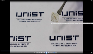
Here is a cool application for ALD demonstrated by Ulsan National Institute of Science and Technology (UNIST), South Korea - Foldable Transistor Arrays Using Reversibly Foldable Interconnects and Stretchable Origami Substrates. Check out the video in the supplemntary information linked below! The Al2O3 was deposited using a LUCIDA D100 ALD reactor form NCD.

Fully-integrated, Bezel-less Transistor Arrays Using Reversibly Foldable Interconnects and Stretchable Origami Substrates

Mijung Kim, Jihun Park, Sangyoon Ji, Sung-Ho Shin, So-Yun Kim, Young-Cheon Kim, Ju-Young Kim and Jang Ung Park

Nanoscale, 2016, Accepted Manuscript
DOI: 10.1039/C6NR02041K
Received 10 Mar 2016, Accepted 10 Apr 2016
 
 
Movie of the  Reversibly Foldable Interconnects and Stretchable Origami Substrates (Link)
 
Here we demonstrate Fully-integrated, Bezel-less Transistor Arrays using stretchable origami substrates and foldable conducting interconnects. Reversible folding of these arrays is enabled by origami substrates which are composed of rigid support fixtures and foldable elastic joints. In addition, hybrid structures of metal thin film and metallic nanowires worked as foldable interconnects which are located on the elastomeric joints.

New Book: Growth and Transport in Nanostructured Materials by Angel Yangas-Gil

Here is a new book on the fundamentals of PVD, CVD and ALD by Angel Yangas-Gil who is a Principal Materials Scientist & Institute Fellow, Northwestern Argonne Institute of Science and Engineering and well known Expert in the ALD community.

Angel Yangas-Gil is a Principal Materials Scientist & Institute Fellow, Northwestern Argonne Institute of Science and Engineering (link)

Growth and Transport in Nanostructured Materials

The Fundamentals of PVD, CVD and ALD

 Yanguas-Gil, Angel

This book will address the application of gas phase thin film methods, including techniques such as evaporation, sputtering, CVD, and ALD to the synthesis of materials on nanostructured and high aspect-ratio high surface area materials. We have chosen to introduce these topics and the different application fields from a chronological perspective: we start with the early concepts of step coverage and later conformality in semiconductor manufacturing, and how later on the range of application branched out to include others such as energy storage, catalysis, and more broadly nanomaterials synthesis.

 The book will describe the ballistic and continuum descriptions of gas transport on nanostructured materials and then will move on to incorporate the impact of precursor-surface interaction. We will finally conclude approaching the subjects of feature shape evolution and the connection between nano and reactor scales and will briefly present different advanced algorithms that can be used to effectively compute particle transport, in some cases borrowing from other disciplines such as radiative heat transfer. The book gathers in a single place information scattered over thirty years of scientific research, including the most recent results in the field of Atomic Layer Deposition. Besides a mathematical description of the fundamentals of thin film growth in nanostructured materials, it includes analytic expressions and plots that can be used to predict the growth using gas phase synthesis methods in a number of ideal approximations. The focus on the fundamental aspects over particular processes will broaden the appeal and the shelf lifetime of this book. The reader of this book will gain a thorough understanding on the coating of high surface area and nanostructured materials using gas phase thin film deposition methods, including the limitations of each technique. Those coming from the theoretical side will gain the knowledge required to model the growth process, while those readers more interested in the process development will gain the theoretical understanding will be useful for process optimization.

Using TMA and HF for Atomic Layer Etching of Al2O3

The semiconductor industry is pushing for Atomic Layer Etching of (ALE) to support CMOS scaling beyond 10 nm. Untill now the main focus have been on plasma activated processes that many times result in anisotrpic etching or non conformal etching like an ALD guy would say. Recently however, Prof. S.M George and his group at Boulder Colorado has presented paths to thermally activated processes for self limited etching using Sn(acac)2 and HF or HF-pyridine. Here, they have progressed further and can actually basically run the most well known ALD precursor - TMA for growing Al2O3 - backwards by using TMA and HF vapour.
 
 
ALE 2016 Ireland, 3rd International Workshop on Atomic Layer Etching, 24th – 25th July 2016, Dublin, Ireland: http://ald2016.com/atomic-layer-etching-workshop-overview/ 
 It will be interesting to see if additional important high-k materials for logic and memory devices such as HfO2 and ZrO2 can be etched using a similar approach. Prof. S.M. George is an invited speaker at the ALE 2016 Workshop in Dublin 24th - 25th of July 2016 and we will have a chance to learn more of this exciting work then!

Trimethylaluminum as the Metal Precursor for the Atomic Layer Etching of Al2O3 Using Sequential, Self-Limiting Thermal Reactions

Younghee Lee, Jaime W. DuMont, and Steven M. George
Chem. Mater., Just Accepted Manuscript
DOI: 10.1021/acs.chemmater.6b00111

Trimethylaluminum (TMA, Al(CH3)3) was used as the metal precursor, together with HF, for the atomic layer etching (ALE) of Al2O3 using sequential, self-limiting thermal reactions. Al2O3 ALE using TMA demonstrates that other metal precursors, in addition to Sn(acac)2, can be employed for Al2O3 ALE. The use of TMA for Al2O3 ALE is especially interesting because TMA can also be used for Al2O3 atomic layer deposition (ALD). Quartz crystal microbalance (QCM) experiments monitored Al2O3 ALE at temperatures from 250-325°C. The Al2O3 ALE was linear versus number of HF and TMA reaction cycles. The QCM studies showed that the sequential HF and TMA reactions were self-limiting versus reactant exposure. The Al2O3 etching rates increased at higher temperatures. The QCM analysis measured a mass change per cycle (MCPC) of -15.9 ng/(cm2 cycle) at 300°C. This MCPC corresponds to an Al2O3 etch rate of 0.51 Å/cycle. X-ray reflectivity and spectroscopic ellipsometry analyses confirmed the linear removal of Al2O3 and etching rates. Fourier transform infrared spectroscopy measurements monitored Al2O3 ALE by observing the loss of infrared absorbance from Al-O stretching vibrations. Surface intermediates were also identified after the HF and TMA exposures. Al2O3 ALE with TMA is believed to occur by the reaction: Al2O3 + 4Al(CH3)3 + 6HF → 6AlF(CH3)2 + 3H2O. The proposed mechanism involves fluorination and ligand-exchange reactions. The HF exposure fluorinates the Al2O3 surface and forms an AlF3 layer and H2O as a volatile reaction product. During the ligand-exchange transmetalation reaction, TMA accepts F from the AlF3 layer and donates CH3 to produce volatile AlF(CH3)2 reaction products. Additional metal precursors for thermal ALE may be possible based on similar fluorination and ligand-exchange reactions.

Sunday, April 10, 2016

PERC Solar Cell Technology 2016 – Background, Status and Outlook for ALD Al2O3

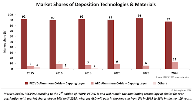
Here si a very good and detailed report by TaiyangNews on PERC solar cell technolygy that is free fo charge to doenload. Thnak you Roger Görtzen at SoLayTec for letting me know about this one. It shows a slow and steady growth for ALD Al2O3 back side passivisation the next 10 years. One of the major concerns for Al2O3 introduction u either PECVD or ALD is the cost of TMA. For ALD the industry seem to worry about that it is a new technoloogy and that you anyway need too cap of the Al2O3 with a silicon based dielectric PECVD process step. 

PERC Solar Cell Technology 2016 – Background, Status and Outlook provides an overview on background, status and outlook of promising high-efficiency silicon-based PERC cell technology.

All solar cell manufacturers that are evaluating capacity expansion in the current investment cycle have to decide if they stick to traditional technology or opt for advanced solutions. The simplest and most attractive silicon cell technology upgrade is called PERC, which stands for Passivated Emitter Rear Cell.


Our new report PERC Solar Cell Technology 2016 – Background, Status and Outlook provides an overview on background, status and outlook of PERC cell technology.
PERC is an advanced silicon cell architecture that comes with a promise of higher efficiencies. At the same time, it requires only minimal changes to existing solar cell processing lines. The concept is not new, it was invented in 1983 by well known Australian scientist Martin Green.
Opting for PERC means to add a rear passivation scheme to standard BSF cell technology. As for the implementation, it involves depositing a rear surface passivation film, which is subsequently opened to give way for formation of a rear contact. In addition, the chemical wet-bench based edge-isolation step is tweaked for rear polishing. The key aspect of PERC technology is to deposit the rear passivation film.
Our study provides background on the different rear passivation materials – the early silicon oxynitride and today state-of-the-art material, aluminum oxide.
The deposition of aluminum oxide can be accomplished by 4 well known deposition technologies that have been tweaked to apply this dielectric. While sputtering tools are currently not being offered for commercial production, there is little demand for APCVD. The two technologies for aluminum deposition mainly considered by commercial cell producers are PECVD and ALD. The study shows the pros and cons for each of these deposition technologies.
The report also delves into product details; nearly every deposition tool supplier is offering a package line for PERC. Short product descriptions are given on p. 29.
While the the first part of the study deals with equipment and material of PERC cells, we have also looked at the efficiencies and the performance potential at commercial scale. As new record efficiencies are quickly changing for PERC, commercialization of the technology is in full swing.
We estimate that 4.9 GW of PERC capacity was installed in 2015, resulting in about 3 GW of PERC cell production. The report also provides an estimate for 2016 PERC production.
Like any other technology, PERC faces challenges. The major concern is the so-called Light Induced Degradation (LID) effect, which, however, is especially associated with multicrystalline PERC cells today, but some companies already have this issue under control. In comparison, we also take a brief look at other high-efficiency cell concepts.
However, our overall impression is: PERC seems to be absolutely ready for prime time.

The Report can be downloaded free of charge here.

Saturday, April 9, 2016

A very warm welcome to RASIRC for sponsoring the ALD News Blog!

A very warm welcome to RASIRC as a new sponsor of the BALD Engineering ALD news blog! RASIRC based in San Diego California specializes in products that generate and deliver gas to fabrication processes. Each unit is a dynamic gas plant in a box—converting common liquid chemistries into safe and reliable gas flow for most processes. First to generate ultra-high purity (UHP) steam from de-ionized water, RASIRC technology can now also deliver hydrogen peroxide gas in controlled, repeatable concentrations.

RASIRC products that are in use for ALD include:
 
 
Next on the CMC Confernce 5-6th of May in Hillsoboro, Dan Alvarez, Chief Technology Officer of RASIRC will present their new technology for Hydrazine delivery in a talk entitled: "Hydrazine as a Low Temperature Nitride Source: Materials Challenges for High Volume Manufacturing"
 
You will be reading more about RASIRC here in the near future!


"ALD for Industry 2017" in Dresden open for Sponsoring & Exhibition

Ladies and Gentlemen,
 
As you may have noticed, Dresden has developed to the German Hotbed for ALD and we want to make you aware of an ALD event in Dresden early 2017 that may be very interesting for you to attend. The event will have a strong Industrial focus for ALD and you will be able to reach out to the German ALD market and your potential and existing customers here. 

This Event is organized in collaboration between members of "ALD Lab Dresden" and EFDS and is now open for Sponsoring & Exhibition booking. We have already had a good response from the ALD Equipment industry so hurry since number of exhibition tables will be limited!


ALD for Industry, 17-18 January 2017, Swissôtel Dresden Am Schloss

"This event provides the opportunity to learn more about fundamentals of ALD technology, to get informed about recent progress in the field and to get in contact with industrial and academic partners. Increase your visibility and present your company in our accompanying exhibition."

http://www.efds.org/appointments-detail/events/ald-workshop-ald-for-industry.html

More information will be available soon! 

Contact for Sponsoring:

Grit Kotschenreuther
kotschenreuther@efds.org
Tel. +49 351 8718372 


Thursday, April 7, 2016

Samsung Starts Mass Producing Industry’s First 10-Nanometer Class DRAM

Samsung just announced that they start Mass Producing Industry’s First 10-Nanometer Class DRAM now. According to the press release (here) the key technology developments include:
  • improvements in proprietary cell design technology
  • QPT - quadruple patterning technology lithography 
  • Ultra-thin dielectric layer deposition.
The two later ones should mean a lot of ALD business for High-k, Electrodes and dielectric spacers.

Below is a DRAM Technology Roadmap published by TechInsights last summer and here you can see that Samsung is nailing it and next we should expect announcements from SK Hynix and The Micron Camp.


Here is an earlier post form IEDM 2015 in December when Samsung revieled some details - if thoose are used here is unknown so hopefully some reverse engineering study will surface next:

Samsung to present low cost manufacturing of 20 nm DRAM and beyond at IEDM2015

Some advancement in keeping low cost manufacturing of 20 nm DRAM will be presented by Samsung at IEDM 2015. Key elements are:

  • avoiding EUV lithography
  • honeycomb structure (see figure below)
  • air-spacer technology


According to Solid State Technology an air-gap spacer arrangement achieves a 34% reduction in bitline capacitance for faster operation.

20nm DRAM: A New Beginning of Another Revolution (Invited), J. Park, Y.S. Hwang, S.-W. Kim, S.Y. Han, J.S. Park, J. Kim, J. W Seo, B.S. Kim, S.H. Shin, C.H. Cho, S.W. Nam, H.S. Hong, K.P. Lee, G.Y. Jin, and E.S. Jung, Samsung Electronics Co.


For the first time, 20nm DRAM has been developed and fabricated successfully without EUV lithography using the honeycomb structure and the air-spacer technology. These low-cost and reliable schemes are promising key technologies for 20nm technology node and beyond.


Plasma ALD 2015 in Review is completed!

Plasma-ALD.com has completed their 2015 review and published all the interesting statistics.  - very interesting stuff showing strong growth of Plasma ALD (PEALD).

"There was a lot of interesting plasma atomic layer deposition activities during 2015. I have found 237 references utilizing PEALD in one form or another that were accepted for publication during the year. That is a 63% increase over the 147 references found in 2014."


Top 3 is unchanged: South Korea, USA and Germany. Taiwan and The Netherlands moving up with a lot of publications in 2015.

Please go here to dig into the numbers: http://www.plasma-ald.com/

Wednesday, April 6, 2016

Beneq to present the most transparent Display and Spatial sheet-to-sheet ALD at ALD2016

Beneq has announced that they are to present the most transparent Display and Spatial sheet-to-sheet ALD at ALD2016. In three presentations at the event they will present the following :
  • Development of the world's most transparent display - enabled by ALD
  • Large area sheet-to-sheet spatial ALD system for high-throughput coating applications
  • ALD based 3D NIR filter and refractive index control for Rugate filters
Read the full story at the Beneq Blog here: http://beneq.com/blog/201604/platinum-presentations.html


ASM F-120 ALD Reactor for sale

Here is a classic ALD reactor for sale and it seems to be a rather new one since it is called ASM F-120 SAT ALCVD(TM) and not Microchemistry. A once in a life time opportunity!

Thanks to Brent Sperling for sharing this one and you can check it out here! on the Craiglist.


Monday, April 4, 2016

New Critical Materials Conference's Powerful Agenda


 Buy Reports  | CMC Fabs   |  CMC Conference  |  Register Now
New Critical Materials Conference's Powerful Agenda
May 5-6, Hillsboro Oregon
The Critical Materials Conference provides a framework to catalyze the flow of "actionable" technical and supply chain information related to critical materials. 

New Additions to the Critical Materials Conference Include: 
  • David Thompson, Ph.D., Director of Process Chemistry of Applied Materials
    • Agony in New Material Introductions - Minimizing and Correlating Variabilities
  • Suresh Ramalingam, Sr. Director, Advanced Packaging Development of Xilinx
    • Packaging Materials - Future Challenges 
A highly differentiated program, with networking opportunities for all attendees. 
For full agenda details click here.

Themes of the Conference are centered around the needs of the Critical Materials Council and the global IC fabrication industry. While executive conferences typically focus on the "what" and "why" of materials technologies, this conference will discuss "how" new materials can be controllably, safely, and cost-effectively used in fabs. The Conference will also include market data to validate "when" materials will be needed. Attendees from fabs, OEMs, and materials suppliers alike will have the opportunity to interact with the presenters and colleagues, to gain insights into best-practices of the entire supply-chain.
 
For more information on the conference go to www.cmcfabs.org/seminars/ 
Great Sponsorship Opportunities available, 
please contact cmcinfo@techcet.com or call 1-480-382-8336

Sponsors and Committee