Monday, April 4, 2016

Novel Negative Capacitance FET using a 5nm hafnium zirconium dioxide ferroelectric layer

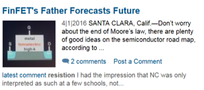
Here is an interesting story in EETimes on how "The Father of FinFET" Prof. Chenming Hu at Berkeley Device Modeling Center is promoting the Negative Capacitance Field efefct Transistor (NC-FET) based on a ferroelectric Hafnium Zirconium oxideintegrated into a standard HKMG Stack. The presenatation was hels as a Key Note "What Else Besides FinFET?" at the SNUG Silicon Valley 2016 · March 30 –31 · Santa Clara Convention Center organized by Synopsys.

http://www.eetimes.com/document.asp?doc_id=1329333&

 The gate stack under investiogation is a conventional thin HfO2 gate oxide with an added 5 nm ferrorelctric ZrO2:HfO2 layer before gate processing, which is a process that could be realized in anz sub 45 nm Fab today assuming you can etch a "thick" high-k gate oxide. The NC-FET development is supported by Intel and TSMC who joined joined, paying $140,000 each.

Chenming Calvin Hu is Distinguished Professor of Microelectronics at University of California, Berkeley. From 2001-2004, he was the Chief Technology Officer of TSMC, world’s largest IC foundry. (Wikipedia.org)

You have followed this Blog may have come across previos stories on the discovery and research on ferroelectric Hf-based metal oxides conducted in Dresden, German by NaMLab, Fraunhofer and Globalfoundries. Below is a small collection of those posts. One of the first materials systems besides Si:HfO2, Al:HfO2 and Y:HfO2 was the ZrO2:HfO2 system investigated by Johannes Müller (Fraunhofer IPMS). If this constallation also hare covering NC-FET, besides the work on FE-FETs and FRAM is not known. In any case, it will be continiously interesting to follow the forgress of ferroelectric ALD HfO2 based materials for novel devices!

Dresden Memory Startup To Debut At Semicon Europa

 FMC has been formed by NaMLab to commercialize the work and has taken over a publicly-funded program that will provide €500,000 (about $565,000) to cover development over the period April 2015 to September 2016. Meanwhile the small group of engineers that have formed the company are looking for early-stage investment and potential partners, Mueller said.

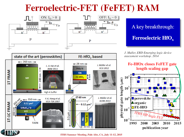
Ferroelectric HfO2 by ALD Key Breakthrough in ITRS “Beyond CMOS” Update 2015


Ferroelectric HfO2 Based Materials and Devices: Current Status and Future Prospects


Qimonda’s late legacy: 28nm FeRAM using ALD Ferroelectric HfO2

“This research goes back to 2007 at DRAM maker Qimonda, when a PhD candidate Tim Böscke was doing research to improve HfO2 as a high-k dielectric for capacitors in dynamic random access memories, using dopants to stabilize the material”, explained Mikolajiick. “At certain dopant concentrations and under specific treatments, Böscke noticed that strange peaks occurred in the CV characteristic of the material, and that it behaved as a ferroelectric. This was totally unexpected!"

Sunday, April 3, 2016

Atomic Layer Deposition at The CMC Conference, 5-6 May, Hillsboro, OR

For those of you that have a chance to attend the CMC Conference coming up in Hilsboro, 5-6th of May here is an updated List of Speakers. We are very happy to announce three key persons in from the ALD industry giving invited talks at this two day event  : 
  • Jean-Marc Girard from Air Liquide
  • S.I. Lee from Veeco
  • David Thompson from Applied Materials

In addtion, a number of invited talks related to ALD by Industry Leaders & Experts:
  • Rob Nine, Strategic Marketing - Pall Microelectronics 
  • Jeff. Hemphill, Sr. Materials Engineer - Intel Corp.
  • John Smythe, Ph.D., Advanced Technology Lead DMTS - MICRON Technologies
  • Max Kelman, Ph.D., Sr. Technology Manager – Aixtron 
  • Dan Alvarez, Ph.D., Chief Technical Officer - RASIRC
Check the schedule below for more details or go directly to the CMC Conference page here: http://cmcfabs.org/seminars/

Day 1, Session II:

Immediate Challenges of Materials & Manufacturing


Day 2, Session III, 1/2 Day:

Emerging Materials Challenges

UPDATE: ALD 2016 Dublin Speakers and Conference Programme


The conference programme for ALD 2016 has been updated with full information on Tutorials and Invited speakers!

Conference Timings:

Sunday 24 July:
Tutorial runs 13:00-17:00 in Convention Centre.  Welcome reception that evening in Guinness Storehouse.
Monday 25 July – Wednesday 27 July:
ALD2016 Conference will open at 8:15 in Convention Centre and closes at 17:45 on Wednesday 27 July followed by a gala dinner on Wednesday evening.


Conference Programme:

Tutorial on Atomic-Layer-Processing, Sunday 24th July:

Click on the speaker name to view their profile:
Speaker Organisation Presentation Title
Sumit Agarwal Colorado School of Mines USA Plasma Physics and Diagnostics
Keren Kanarik Lam Research, USA Overview of Atomic Layer Etching
Fred Roozeboom TU Eindhoven, The Netherlands Processing for 3D-IC Technologies
Sean Barry Carleton University, Canada ALD Precursor Design & Synthesis
Massimo Tallarida Alba, Spain, Characterization of ALD processes and Materials using Synchrotron Light
Annelies Delabie IMEC, Belgium Atomic layer processing of 2D materials for beyond CMOS applications
Stephan Wege Plasway GmbH, Germany Plasma Processing Reactor Design

Invited speakers:

Speaker  Organisation  Presentation title
Raymond Adomaitis University of Maryland Reaction Network Analysis for ALD Processes
Robert Clark TEL America
Byung Joon Choi Seoul National University of Science and Technology Multi-layered selector and switch devices enabled by atomic layer deposition for crosspoint memory
Mike Cooke Oxford Instruments
Jolien Dendooven University of Ghent Synchrotron-based characterization of Pt ALD
Michael Gros-Jean STMicroelectronics
Joseph Hupp Northwestern University
Ying-Bing Jiang University of New Mexico / Angstrom Thin Film Technologies LLC, USA
John Langan Air Products
Anatollii Malygin St Petersburg State Technological Institute
Yongfeng Mei Fudan University
Lars Samuelson Lund University Nanowire-based Technologies for Electronics, LEDs and Solar-cells
Further speakers, profiles and the conference programme will be published soon.  Please check back for information.

SoLayTec receives new ALD tool orders from PV solar cell manufacturers

SoLayTec today announced the continuing positive trend of incoming orders. Four new solar customers around the globe have ordered the Atomic Layer Deposition (ALD) equipment from SoLayTec. One of these customer is from Taiwan, and a mayor a step to open further opportunities for SoLayTec in this market. These shipments are scheduled to start within this quarter.

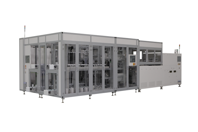
Depending on the capacity levels that are needed SoLayTec offers three types of InPassion ALD. Main difference is the number of deposition units modules added in such a system. The basic three products offered are 4, 6 or 8 deposition units, that respectively result into 2,500* wph, 3,600* wph or 4,800* wph. (www.solaytec.com)
Depending on the capacity levels that are needed SoLayTec offers two types of InPassion ALD. Main difference is the number of deposition units modules added in such a system. The basic two products offered are 4, 6 or 8 deposition units, that respectively result into 2,500* wph, 3,600* wph or 4,800* wph. - See more at: http://www.solaytec.com/products/inpassion-ald#sthash.y20MGE3A.dpuf
“After several years of having InPassion ALD systems in mass production at multiple customers in China and Japan, SoLayTec is delighted to announce that in the last couple of weeks 3 orders were received”, according Roger Görtzen, co-founder of SoLayTec and manager marketing and sales.


Field Replaceable Unit (optional FRU) - If one of the deposition units is not working properly and can’t be fixed by the customer or SoLayTec service team, this module or FRU will be replaced by another FRU. In this way the tool will be running as fast as possible at 100% capacity again. In parallel this FRU will be send to a SoLayTec service station to be refurbished.
  (www.solaytec.com)
“These machines will be used for production of high efficient solar cell concepts, like p-type PERC, n-type IBC and bi-facial cells. In the past SoLayTec announced that spatial ALD results in a higher efficiency of about 0,2% for multi and mono PERC cells compared to PECVD AlOx. At one leading PV solar cell manufacturer we have measured for ALD Al2O3 a surface recombination velocity between 1- 5cm/sec compared to ≥ 30cm/sec on similar material for PECVD AlOx . This data confirms that the passivation quality of ALD Al2O3 is factor ≥ 6 higher compared to PECVD AlOx. Recently, the c-Si wafer quality has been improved, and this results into better bulk material of the c-Si material. Consequently our customers request an excellent surface passivation which can be provided by ALD Al2O3 for their future cell concepts.” according Roger Görtzen. 
“So far, our customers were located in China, Japan and Europe so we are very happy with our newest market entrance in Taiwan. Now we have finally achieved this important milestone and of course SoLayTec will focus on further expansion of its footprint in this country.” said Roger Görtzen.

SoLayTec

SoLayTec is a spin-off company of the Dutch research organisation TNO and established in 2010. SoLayTec is part of the Amtech Group (Nasdaq ASYS). The company develops, delivers and services machines for atomic layer deposition (ALD) on solar cells worldwide. The SoLayTec ALD machines are designed for mass production in the solar market. In the field of solar cell ALD equipment, SoLayTec has a leading position.

For more information, please visit www.solaytec.com.

Thursday, March 31, 2016

Precursor saving ALD Method from University of Alberta

Here is a clever paper from University of Alberta on how to save expensive ALD precursor in ALD processing by using a burst of  shorter multiple precursor pulses. I´ve seen this approached used in 3D conformal growth in extreme high aspect ratio structures before, but I just had a simple picture in my mind how it works. Here it is explained an proven by experimental work in great detail! 

The approach is also in one sense similar to the Genus process that ran the ALD pulses in undersaturation and was very much faster and precursor saving than "normal ALD". However not that good in extreme aspect ratio structures. The method developed by Triratna Muneshwar should not have this restriction since it works in saturation mode.


University of Alberta materials engineering postdoctoral fellow Triratna Muneshwar and materials engineering professor Ken Cadien have developed a new method for ALD that saves expensive precursors. The paper in Journal of Applied Physics is highlighted here in EurekAlert. On the picture the gentlemen stands in front of a ALD machine from Kurt J. Lesker, which I assume has been used for the experimental verification of the numerical method.

AxBAxB… pulsed atomic layer deposition: Numerical growth model and experiments

Triratna Muneshwar and Ken Caddie
J. Appl. Phys. 119, 085306 (2016); http://dx.doi.org/10.1063/1.4942439

Atomic layer deposition(ALD) is widely used for the fabrication of advanced semiconductor devices and related nanoscale structures. During ALD, large precursor doses (>1000 L per pulse) are often required to achieve surface saturation, of which only a small fraction is utilized in film growth while the rest is pumped from the system. Since the metal precursor constitutes a significant cost of ALD, strategies to enhance precursor utilization are essential for the scaling of ALD processes. In the precursor reaction step, precursor physisorption is restricted by steric hindrance (mA1) from ligands on the precursor molecules. On reaction,some of these ligands are removed as by-products resulting in chemisorbed species with reduced steric hindrance (mA1 → mA2, where mA2 < mA1) and some of the initially hindered surface reaction sites becoming accessible for further precursor physisorption. To utilize these additional reaction sites, we propose a generalized AxBAxB… pulsed deposition where the total precursor dose (ΦA) is introduced as multiple x (x > 1, x ∈ I) short-pulses rather than a single pulse. A numerical first-order surface reactionkinetics growthmodel is presented and applied to study the effect of AxBAxB… pulsed ALD on the growthper cycle (GPC). The model calculations predict higher GPC for AxBAxB… pulsing than with ABAB… deposition. In agreement with the model predictions, with AxBAxB… pulsed deposition, the GPC was found to increase by ∼46% for ZrN plasma enhanced ALD (PEALD), ∼49% for HfO2 PEALD, and ∼8% for thermal Al2O3ALD with respect to conventional ABAB… pulsed growth.

Wednesday, March 30, 2016

Picosun’s ALD solutions at Imec transform battery technology

ESPOO, Finland, 30th March, 2016 – Picosun Oy, the leading supplier of advanced ALD (Atomic Layer Deposition) thin film coating technology, now provides ALD equipment to transform battery manufacturing. 
 
The sustainable energy economy of the future, greener transportation, and the increasing number of portable, mobile and personal electronic devices all require improved means for local energy storage. Nanostructured, solid-state thin film batteries offer a disruptive solution for this. Replacing traditionally used liquid materials in the battery with all solid layers improves the battery safety and lifetime. Thin and flat geometry makes the batteries easily integrated in e.g. wearable electronics, whereas their nanoscale tailored internal structure enables high energy storage capacity.

ALD is an ideal way to prepare the highly conformal, dense, uniform, and structurally and chemically exactly controlled functional layers in the core of the battery stack. Using PICOSUN™ ALD equipment, imec, Belgium, has now developed a solution to deposit a novel, solid electrolyte for lithium ion thin film batteries.

“Our aim at Picosun is to utilize ALD technology for better tomorrow. For example, faster and smoother data handling and communications, and the increasing number of mobile, wearable personal health monitoring devices require compact, efficient, and reliable power delivery solutions. The ALD technology we have now developed with imec for manufacturing of safe and long-lasting thin film batteries is an important breakthrough into a huge market area still relatively new to ALD. We are happy to provide the latest manufacturing solutions to our customers in this field and to see their most advanced products powering our everyday electronics,” states Juhana Kostamo, Managing Director of Picosun.

Tuesday, March 29, 2016

Atomic/Molecular Layer Deposition of Lithium Terephthalate for Li-Ion Battery Anodes

EurekAlert.org reports: When microbatteries are manufatured, the key challenge is to make them able to store large amounts of energy in a small space. One way to improve the energy density is to manufacure the batteries based on three-dimensional microstructured architectures. This may increase the effective surface inside a battery- even dozens of times. However, the production of materials fit for these has proven to be very difficult.


Aalto University Researchers testing the material on coin cells. (Mikko Raskinen / Aalto University)

Researches at Aalto University, Helsinki Finland, has develooped a ALD/MLD deposition process for Li-terephthalate, which has been published in Nanoo Letters (below).

- ALD is a great method for making battery materials fit for 3D microstructured architectures. Our method shows it is possible to even produce organic electrode materials by using ALD, which increases the opportunities to manufacture efficient microbatteries, says doctoral candidate Mikko Nisula from Aalto University. (EurekAlert.org)

Atomic/Molecular Layer Deposition of Lithium Terephthalate Thin Films as High Rate Capability Li-Ion Battery Anodes

Nano Lett., 2016, 16 (2), pp 1276–1281


We demonstrate the fabrication of high-quality electrochemically active organic lithium electrode thin films by the currently strongly emerging combined atomic/molecular layer deposition (ALD/MLD) technique using lithium terephthalate, a recently found anode material for lithium-ion battery (LIB), as a proof-of-the-concept material. Our deposition process for Li-terephthalate is shown to well comply with the basic principles of ALD-type growth including the sequential self-saturated surface reactions, a necessity when aiming at micro-LIB devices with three-dimensional architectures. The as-deposited films are found crystalline across the deposition temperature range of 200–280 °C, which is a trait highly desired for an electrode material but rather unusual for hybrid inorganic–organic thin films. Excellent rate capability is ascertained for the Li-terephthalate films with no conductive additives required. The electrode performance can be further enhanced by depositing a thin protective LiPON solid-state electrolyte layer on top of Li-terephthalate; this yields highly stable structures with capacity retention of over 97% after 200 charge/discharge cycles at 3.2 C.

Monday, March 28, 2016

NCD, a fast growing Korean ALD Equipment manufacturer for High Volume manufactuiring


As announced some weeks ago I am happy to have NCD as sponsor for the BALD Engineering ALD News blog. Here a review of the company and its fantastic ALD products follows and you should check the recently updated web page (http://www.ncdtech.co.kr/). NCD Co., Ltd. from Daejeon in Korea is a young and growing company founded in 2010 and is specialized in ALD original equipment manufacturing, which has been covered here on the ALD blog previously (here).


NCD is focusing on equipment development, process development, coating services, and process consulting for advanced ALD technologies for four business areas:

1. Solar
2. Display
3. Semiconductor
4. R&D

NCD has already had quite some successful years in entering the ALD equipment market and has built a very impressive customer base in Asia with main focus on the Korean domestic market, Japan, China and Taiwan.

As you may know, one of disadvantages of ALD is slow growth rate at typically an Å / cycle or so, that is to say ALD has a low throughput. In order to solve this problem, NCD has applied for patents for the high-throughput, high-volume and large-area every year. Based on these patents, NCD have developed their high-volume and large-area ALD system.

Here follows an overview of the ALD technology and equipment offering by NCD

1) High-volume ALD
   - GS ALD : surface passivation for c-Si solar cell                                                                         
   - MC ALD : dielectric for capacitor and encapsulation for micro display (OLED)

2) Large-area ALD
   - TS ALD : buffer layer for CIGS solar cell
   - GD ALD : encapsulation for OLED
LucidaTM GS1200 ALD with automation system

NCD has paved the way for high volume manufacturing by a range of ALD systems (see above). Worth highlighting here is especially the Lucida™ GS1200 ALD system applied for high efficiency solar cells at both Hyundai Heavy Industries and LG Electronics etc. The GS series from NCD can realize Passivation for c-Si solar cell at an impressive through put of >3400 wph @ 10nm-Al2O3.

For the large area CIGS thin film soar and OLED display market, NCD has developed two main platforms - the TS and the GD series respectively. ALD chamber clustering is an approach used by many rather than large stand-alone batch tools. 
LucidaTM GD600 ALD in R&D Lab.

Lucida™ GD series already had been applied to R&D centers of Korean and other customers, and showed the excellent performance for thin film encapsulation (TFE) and barrier applications. NCD is currently possible to run customer demoes with the large size of panel (1500mm x 1800) for using LucidaTM GD600 in the demo room (see above). NCD is the only place to do superior ALD demoes with that size panel.

It will be very exciting to follow NCD the next years when the ALD market continues its growth in many high-volume and large-area ALD applications.