%20(1).png)
High mobility Germanium is one of the most promising channel materials for future Logic, perhaps even at 7nm. Here is an open source paper (see abstract below) on using TEMAHf/H2O process for growing high symmetry cubic HfO2 on high mobility Germanium channel. It´s a joint work by University of Tokyo, Japan, and Zhejiang University, China. Until now all silicon based channel gate dielectrics are typically performed by using the HfCl4/H2O process. However, now moving too alternate high mobility channel materials like Germanium, InGaAsand other III/Vs it seem that the gate stack people will revisit the MO-precursors again - interesting!
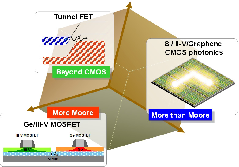
The Takagi-Takenaka group researches the post-scaling semiconductor
devices for low-power LSI and on-chip optical interconnection for: Ge/III-V MOSFETs, Tunnel FETs, Si photonics, III-V CMOS photonics, Graphene photonics and 2D material electronics (from Takagi and Takenaka Group)
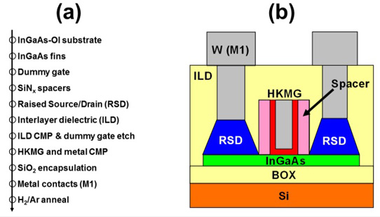
Low temperature formation of higher-k cubic phase HfO2 by atomic layer deposition on GeOx/Ge structures fabricated by in-situ thermal oxidation
We have demonstrated a low temperature formation (300 °C) of higher-k HfO2 using atomic layer deposition(ALD) on an in-situ thermal oxidation GeOx interfacial layer. It is found that the cubic phase is dominant in the HfO2film with an epitaxial-like growth behavior. The maximum permittivity of 42 is obtained for an ALD HfO2film on a 1-nm-thick GeOx form by the in-situ thermal oxidation. It is suggested from physical analyses that the crystallization of cubic phase HfO2 can be induced by the formation of six-fold crystalline GeOxstructures in the underlying GeOx interfacial layer.