Wednesday, May 22, 2019

Picosun provides the leading thin film coating solutions for medical industries

(Picosun, 21 May 2019) Picosun is the leading provider of AGILE ALD™ (Atomic Layer Deposition) thin film coating technology for healthcare industries. Picosun’s biocompatible ALD coatings enable safer and longer lasting products, more compact sensing, therapeutic, and analysis devices, and novel medical applications such as micro implants, smart ablation catheters, and deep brain stimulation probes. Picosun’s PicoMEDICAL™ ALD solutions are already in production use in healthcare industries in depositing bioactive coatings on surgical implants and functionalizing the surface of drug particles for controlled drug delivery.
Application examples:

Dental and orthopedic implants, surgical fixators Read more 

•    Improved osteointegration with bioactive TiO2 thin films
•    Biobarriers for encapsulation against metal ion leakage into tissue fluid


Pacemakers and other implantable electronic devices, microimplants Read more 
  • Hermetic biobarrier encapsulation of the device electronics against the effect of tissue fluid
Others
  • Medical MEMS, sensors, and Lab-on-a-Chip devices
  • Controlled/targeted drug delivery
  • Hydrophobic/hydrophilic coatings
  • Functional coatings on powder materials
  • Extremely thin films on stents

The PICOSUN™ P-300B and P-1000 large-scale batch ALD systems are specially designed for coating surgical implants, implantable medical devices, microimplants, and medical MEMS, sensors, and Lab-on-a-Chip devices.

Friday, May 17, 2019

Foldable Laptops Are On Their Way To Hit The Market By 2020 With Lenovo’s Unveiling Of The World’s First Foldable Laptop

ALD is know to be used in the OLED foldable display manufacturing as a moisture barrier mainly for foldable smartphones and other mobile devices. It’s not been many days of Samsung and Huawei unveiled their first foldable smart-phones: The Galaxy Fold and Mate X, respectively. Now Lenovo is jumping on board with a foldable laptop prototype in its ThinkPad X1 family powered by an Intel processor. For now, it’s just a prototype, but Lenovo may launch it for sale by 2020. The official visual preview can be seen here
 
 
Engadget (Youtube.com) "We got a chance to get our hands on Lenovo's new early prototype foldable PC. This device has some familiar features like an OLED screen and Bluetooth keyboard, but unlike other 2-in-1 laptops, the entire device can fold in half. This lets it fold up to around the size of a paper notebook for easy transport, or even lets you turn the bottom half into a keyboard you can type on. This is still early tech, but it's a look at what portable devices could be in the near future."
The prototype is with a 13.3″ screen that you can fold into the size of a compact 9.6″ Moleskine notebook. The laptop can be unfolded entirely and you can use the built-in kickstand on the rear to keep the screen standing up. You can also connect a Bluetooth keyboard to the device to use it as a traditional laptop; or, you can also just fold the screen halfway, and place it down on a table to use the bottom half as a virtual keyboard for typing. An attached stylus from Wacom can be utilized for super-accurate touch input or for virtual ink. The laptop also employs an attractive OLED screen (2K screen resolution, 4:3 aspect ratio) manufactured by LG display.


Lenovo doubles the number of hinge cycles it tests for its laptops to prevent the wear down of the foldable mechanism over time. Because it is under the ThinkPad name, the product will still need to pass Lenovo’s “rigorous” testing for ThinkPad category to ensure it’s just as durable. This is a Windows-based device, and Lenovo is working with Microsoft to make sure the software experience is optimized for this foldable format, for example, swapping to different modes needs to be seamless, and Windows needs to improve its tablet and touch interface to add value to this product. Moreover, the laptop has stereo speakers, an infrared camera, and two USB-C ports. Lenovo also claims it will offer an “all-day battery,” but there is no numeric figure out yet. 
 
A patent application has just been published by the US Patent and Trademark Office, which comprises a foldable notebook with an OLED screen and a keyboard portion. Lenovo (Singapore) Pte. Ltd. US20190011955 DEVICE WITH FOLDABLE DISPLAY (LINK)
 
However, last Thursday, a senior Intel executive told the Nikkei Asian Review that the foldable laptops are at least two years away. "It's early path-finding now, and we are trying to understand the capability and the limitation of the [foldable] technology," Joshua D. Newman, Intel's general manager of mobile innovation and vice president of the company's Client Computing Group, said Wednesday on the sidelines of an Intel symposium in Taipei. (Link
 
----------
By Abhishekkumar Thakur and Jonas Sundqvist


Wednesday, May 15, 2019

RASIRC Enables Low Temperature Group III Metal-Nitride Deposition

Company highlights use of a novel hydrazine source at Compound Semiconductor Week

San Diego, Calif – May 15 2019 – RASIRC will introduce a novel hydrazine delivery system for reduced temperature Group III Metal-Nitride deposition at the Compound Semiconductor Week 2019 Workshop (CSW), Nara, Japan held May 19-23. RASIRC Chief Technology Officer Dr. Daniel Alvarez will present “Enabling Low Temperature Aluminum Nitride ALD by Use of a Novel Hydrazine Source” during the event’s poster session on May 21. The poster will compare growth characteristics and film properties for TMA/Brute Hydrazine versus TMA/Ammonia.

“There is an emerging need for low temperature III-Nitride deposition in order to prevent unwanted atomic diffusion of nearby metals and metal alloys. Utilization of hydrazine is thermodynamically more favorable due to the reactive nature of the N-N bond,” says Alvarez. “Hydrazine has been available commercially for many years, but not in a pure enough form needed for semiconductor manufacturing.” 


BRUTE Hydrazine Gas Superior to Standard 'anhydrous' hydrazine, which has a water concentration ranging from 0.2-2.0%. BRUTE Hydrazine has purity levels of less than 50ppm in the liquid phase and less than 1.0ppm in the gas phase. This makes BRUTE Hydrazine purity levels comparable to semiconductor grade ammonia. A higher reactivity compared to ammonia enables lower resistivity TiN films to be deposited by ALD at lower temperatures, which is essential for High-k/Metal Gate technology and metallization barrier/seed layers by ALD (Product description, LINK).


RASIRC President and Founder Jeffrey Spiegelman adds, “The use of hydrazine will enable our customers to have larger process windows while reducing costly precursor consumption found with sources like Indium.”

CSW Workshop is a joint venue for the 46th International Symposium on Compound Semiconductors (ISCS) and the 31st International Conference on Indium Phosphide and Related Materials (IPRM). ISCS is an international conference focusing on III-V, II-VI and IV-IV semiconductors and covers the scope of a variety of compound semiconductors used in modern electronic devices. IPRM is known as the leading worldwide conference on indium phosphide and related materials, from physics to its applications.

Dr. Alvarez will be available throughout the event to discuss the RASIRC precursor chemistry product line-up, which includes hydrazine, hydrogen peroxide and more. Information about RASIRC products will also be available in the Taiyo Nippon Sanso Corporation (TNSC) exhibition stand.

About RASIRC Products

BRUTE® Hydrazine enables uniform nitride deposition for Silicon and early transition metals at low temperature. BRUTE Hydrazine may also be used as an atomic hydrogen source, where metals such as Ru, Cu, and Co may be cleaned and reduced. Hydrazine gas is generated in situ and is virtually water free. Brute Hydrazine has been formulated for a relatively high flash point for safer handling.

BRUTE Peroxide is a novel oxidant that improves nucleation density at film interfaces when compared to other oxidants. Surface functionalization is more dense, and initiation is faster using anhydrous hydrogen peroxide gas compared with alternatives. This enables better selectivity and less damage to metal surfaces in ASD processes.

RASIRC Peroxidizer® provides high volumes of reactive H2O2/H2O mixtures for high throughput ALD. This reactive gas generator is ideal for roll-to-roll ALD coatings that require high speed deposition at reduced temperatures.

Additional RASIRC products include the RainMaker® Humidification System (RHS) and the Hydrogen Peroxide Steamer (HPS). The RHS generates water vapor for oxidation applications, and the HPS provides surface cleaning, preconditioning, wet thermal oxidation, and residual carbon removal.

About RASIRC RASIRC specializes in products that generate and deliver gas to fabrication processes. Each unit is a dynamic gas plant in a box — converting common liquid chemistries into safer and reliable gas flow for most processes. RASIRC technology delivers water vapor, hydrogen peroxide gas, and hydrazine gas in controlled, repeatable concentrations. RASIRC gas delivery systems, humidifiers, and closed loop humidification systems are critical for many applications in semiconductor, photovoltaic, pharmaceutical, medical, biological, fuel cell, and power industries. Call 858-259-1220, email info@rasirc.com or visit http://www.rasirc.com.

Sunday, May 12, 2019

Intel 2019 Investor Meeting: 7 nm Product in 2021

Intel held its 2019 investor meeting May 8, 2019 (LINK), it's first since 2017, and CEO Bob Swan announced that Intel would launch its 7 nm process in 2021 to challenge TSMC's 5 nm products.

Intel's Xe graphics will be the leading 7 nm product, which will come on the heels of Intel's first discrete 10 nm GPU that arrives in 2020. The company also unveiled its first block diagram of the Ice Lake architecture and announced that its new 10nm Tiger Lake processors will come to market in 2020.
Source: Tom´s Hardware LINK

 (intel.com)

----------
By Abhishekkumar Thakur

Wednesday, May 8, 2019

4th CMC Conference Enabled Critical Information and Connections

Fab materials event in Albany, New York area April 25-26 featured GlobalFoundries keynote and Intel and TI presentations. Plan now for the 2020 April 23-24 event in Hillsboro, Oregon. 

(SAN DIEGO (PRWEB) May 07, 2019) Over 150 leading executives and managers within the semiconductor manufacturing ecosystem gathered on April 25th and 26th in the Albany area of New York state for an important event on fabrication (fab) materials. The fourth-annual Critical Materials Council (CMC) Conference, produced by TECHCET, included topical presentations, a fab tour, exhibits by specialty materials suppliers, and networking roundtable discussions to learn about best-practices in a pre-competitive environment. Folks who missed attending the event this year can register to access the posted presentations for a nominal fee at https://cmcfabs.org/cmc-conference-2019/.

The event opened again, as in each of the prior three years, on an extremely strong business and technology keynote address by an executive from one of the CMC Fab member companies. The 2019 CMC Conference keynote was given by Dr. John Pellerin, Deputy CTO and VP of Worldwide R&D, GlobalFoundries. Pellerin talked about how demand for new high-volume manufacturing (HVM) semiconductor devices over the next few years will drive needs for increased numbers of new specialty materials as well as volumes of existing materials in his presentation on "Materials Challenges & Opportunities in Differentiated Technologies."

In the first session of the event covering global supply-chain issues of economics and regulations, G. Dan Hutcheson, CEO of VLSI Research, presented on "Slowdown: When did it start? What drove it? And When will the recovery come?" Hutcheson showed data from leading economic indicators that the recent decline in global semiconductor fab industry revenues due to memory chip prices may have already turned around.

TECHCET Sr. Analysts Dr. Jonas Sundqvist and Terry Francis presented updated information on demand drivers and forecasts for ALD/CVD precursors and Rare Earths, respectively. Sundqvist--also leader of the Thin Film Technologies Group at Fraunhofer IKTS--focused on how new 3D memory and logic chips demand more deposition precursors such that chemical volume growth will outpace that of silicon wafers, shown in the Figure. Francis showed how "Rare Earth" elements are not so rare at the elemental level, but complex dynamics between mining and refining and capitalism have led to a situation where mainland China currently controls most of the market for elements such as lanthanum (used in advanced ICs to create CMOS logic gates). Deep dives into all such materials matters are found in the TECHCET Critical Materials Reports (CMR), and you can find all of them online at https://techcet.com/shop/

Global semiconductor silicon quarterly wafer shipments 2015-2019 in millions of square inches (MSI). (Source: TECHCET)
The 2020 spring CMC Conference is scheduled for April 24-25 in Hillsboro, Oregon. The CMC Fab members and Associate members will again gather for two days of private face-to-face meetings before attending the public CMC Conference.

In addition to the annual spring CMC Conference in the US, there is also an annual fall CMC Seminar in Asia. The 2019 CMC Seminar will be held on October 17 in Taoyuan, Taiwan. For more information on CMC events see https://techcet.com/cmc-events/.

About CMC:
The Critical Materials Council (CMC) of Semiconductor Fabricators (CMCFabs.org) is a membership-based organization that works to anticipate and solve critical materials issues in a pre-competitive environment. The CMC is a business unit of TECHCET, and includes materials supplier Associate Members.

About TECHCET:
TECHCET CA LLC is an advisory services firm focused on process materials supply-chains, electronic materials business, and materials market analysis for the semiconductor, display, solar/PV, and LED industries. Since 2000, the company has been responsible for producing the SEMATECH Critical Material Reports™, covering silicon wafers, semiconductor gases, wet chemicals, CMP consumables, Photoresists, and ALD/CVD Precursors. For additional information about reports, market briefings, CMC membership, or custom consulting please contact info(at)cmcfabs(dot)org, +1-480-332-8336, or go to http://www.techcet.com or http://www.cmcfabs.org.

Tuesday, May 7, 2019

Demand for ALD equipment and Lumineq displays grows at Beneq

Beneq invests in R&D and production at the Home of ALD

Beneq®, a leading supplier of Atomic Layer Deposition (ALD) equipment and coating services, and the world’s premier manufacturer of thin film electroluminescent displays, has introduced a new investment plan to support growth in new industrial ALD solutions and the transparent display business. 

Following the agreement about the acquisition of Beneq Oy in September 2018, it was announced today that the new owners of Beneq have approved an investment program that allows Beneq to grow faster in its strategic focus areas, such as ALD solutions for the emerging semiconductor applications and transparent vehicle displays. 
 
 
Together with the new owners’ earlier investments in 2018 to improve Beneq’s equity ratio and working capital, the announced development programs result in a total investment of over 20 million euros. 

“When we invested in Beneq, we invested in people, technology know-how and innovation. The new growth plan will help us to realize the potential and achieve the ambitious growth targets we have set for Beneq,” commented Kong Jun, Chairman of Beneq.

New high-volume ALD manufacturing solutions for More-than-Moore applications

For the Atomic Layer Deposition business unit, the new growth program means major investments in new ALD solutions for the emerging semiconductor ALD business applications in the area of the so called More-than-Moore applications, such as MEMS, image sensors, power semiconductors and RF components needed for the future 5G and IoT solutions.

“Emerging semiconductor ALD and the diversified More-than-Moore applications are an extremely promising growth area for us. We have already had success in these areas with our latest flexible ALD cluster tools for high volume manufacturing. The new investment plan will allow us to fast-track our product development and services in these markets,” said Tommi Vainio, Vice President, Atomic Layer Deposition of Beneq.

Transparent displays for the automotive and transportation industries

For Lumineq Displays, the display business unit of Beneq, the investment plan allows both acceleration of product development in the area of transparent and in-glass displays, and improvements in Beneq’s display factory in Espoo, Finland.

“We have seen great interest in our transparent in-glass displays, especially in the transportation and automotive industries. The window-like transparency of Lumineq displays has helped our customers to build vehicles with improved safety and user experience and will serve as an important differentiation factor in their products,” said Petri Schroderus, Vice President, Lumineq Displays.

A recruitment campaign to support future growth

To enable future growth, Beneq has a continuous program to attract new talent. With the investment plan now approved, the company will start the next large recruitment campaign for building the talent pool. Most of the new positions will be in Espoo, Finland, but the plan also includes recruitment for Beneq’s international teams.


Applied Materials - The AI Era is Driving Innovations in Memory

[Applied Materials Blog] Industries from transportation and healthcare to retail and entertainment will be transformed by the Internet of Things, Big Data and Artificial Intelligence (AI), which Applied Materials collectively calls the AI Era of Computing.

The previous computing eras—Mainframe/Minicomputer, PC/Server and Smartphone/Tablet—all benefitted from advances in Moore’s Law whereby 2D scaling was accompanied by simultaneous improvements in performance, power and area/cost—also called “PPAC.”

While AI Era applications are booming, Moore’s Law is slowing; as a result, the industry needs breakthroughs beyond 2D scaling to drive PPAC in new ways. Specifically, we need new computing architectures, new materials, new structures—especially area-saving 3D structures—and advanced packaging for die stacking and heterogeneous designs.
 

The AI Era is Driving a Renaissance in Semiconductor Innovation (Applied Materials Blog)
 
AI Era architectural changes are influencing both logic and memory. Machine learning algorithms make heavy use of matrix multiplication operations that are cumbersome in general-purpose logic, and this is driving a move to accelerators and their memories. AI compute includes two distinct memory tasks: first, storing the intermediate results of calculations; and second, storing the weights associated with trained models.

Performance and power are important in the cloud and in the edge, and innovations in memory can help. One approach using existing memory technologies is “near memories” whereby large amounts of working memory are condensed, placed in close physical proximity to logic, and connected via high-speed interfaces. As examples, 3D stacking and through-silicon vias are gaining traction. One major drawback of SRAM and DRAM as “working memories” in these applications is that they are volatile and need a constant supply of power to retain data—such as weights.

To reduce power in the cloud and edge, designers are evaluating new memories that combine high performance with non-volatility so that power is only needed during active read and write operations. Three of the leading new memory candidates are magnetic random-access memory (MRAM), phase-change RAM (PCRAM) and resistive RAM (ReRAM). 

Full article: Applied Materials Blog LINK
 
Additional read: Manufacturing Requirements of New Memories LINK

Tuesday, April 30, 2019

Improving SAQP Patterning Yield using Virtual Fabrication and Advanced Process Control

Here is a noceanimation and descrioption of the Self-Aligned Quadruple Patterning (SAQP) from Coventor.
 
[Coventor] Advanced logic scaling has created some difficult technical challenges, including a requirement for highly dense patterning. Imec recently confronted this challenge, by working toward the use of Metal 2 (M2) line patterning with a 16 nm half-pitch for their 7nm node (equivalent to a 5nm foundry node). Self-Aligned Quadruple Patterning (SAQP) was investigated as an alternative path to Extreme Ultra-Violet (EUV) lithography for this line patterning application. At the 2019 SPIE Advanced Lithography conference, Coventor personnel demonstrated how virtual process modeling (combined with advanced process control) could provide enhanced patterning yield and enable SAQP patterning at this tight pitch (See Complete White Paper).
 
Source: Coventor LINK
 

Monday, April 29, 2019

Millennium-Technologiepreis 2018 gewinner Dr. Tuomo Suntola kommt nach Dresden

 
Millennium-Technologiepreis 2018 gewinner Dr. Tuomo Suntola kommt nach Dresden - Keynote bei V2019 9. Oktober 2019. Er entwickelte innovative Technologie der Atomlagenabscheidung.

Helsinki, 22. Mai 2018. Die vom finnischen Physiker Tuomo Suntola entwickelte innovative Technologie der Atomlagenabscheidung (atomic layer deposition, ALD) ermöglicht uns ein Leben mit hocheffizienten IT-Produkten und sozialen Medien. Die ALD-Technologie bietet zudem Einsatzmöglichkeiten in den Bereichen Medizin und nachhaltige Energie. Der Präsident der Republik Finnland, Sauli Niinistö, überreichte den achten Millennium-Technologiepreis am 22.5.2018 in Helsinki.

Link: https://news.cision.com/de/technology-academy-finland--taf-/r/der-finnische-physiker-tuomo-suntola-erhalt-den-millennium-technologiepreis-2018-fur-seine-innovatio,c2524413
 
V2019 – Vakuum & Plasma Oktober 8-10
Vorträge und Diskussionen, Neuigkeiten und Trends und Themenschwerpunkte:
  • Energie
  • Bio & Medizin
  • Optik
  • Verschleißschutz
  • ALD (Vorlesung, Poster, Workshop)
Link: https://www.efds.org/event/v2019-vakuum-plasma/

Sunday, April 28, 2019

China’s water crisis stems the flow of zirconium and rare earths for global industries

World Water Day on 22nd March highlighted some staggering facts about water shortages affecting much of the world’s population. While many Western countries take access to clean water for granted, growing water crises in other countries have world-wide consequences. For example, China is taking steps to secure its water resources, with severe impacts for global supply chains across multiple industries.

‘Our bodies, our cities and our industries, our agriculture and our ecosystems all depend on it,’ said UN Secretary-General António Guterres. 70-80% of all water consumption is for agriculture and energy production. Balancing the water needs of food and energy production is a challenge for many nations.

Water is also essential to mining, chemicals production, and manufacturing, industries which have long assumed ongoing, plentiful supply. This perception is changing as a deeper understanding of the water balance for each country reveals a different reality. Some countries, including China, are net water exporters: the water used to produce the goods and materials they export is higher than the water embodied in imports. Also, the production of exports often pollutes their waterways.

As water stress sets in, these countries have no choice but to change their production practices and trade balance, disrupting global supply chains. For the past five years, the World Economic Forum has ranked water crises in its top 5 global risks in terms of impact, yet most industrial companies seem oblivious to the risks to supply chains for themselves and their customers.

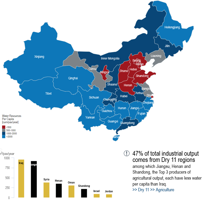
Some provinces have water resources on par with the Middle East. Source: CWR LINK 

Graphic media images of devastating floods from typhoons and other extreme weather events give the impression that China has plenty of water. In southern China, this is partially true, but it’s not so in the north. According to China Water Risk, the 11 driest provinces are in northern China. Home to 38% of the population, these provinces account for 36% of agricultural output, 47% of industrial output and 43% of GDP, yet have only 7% of the country’s water resources. With a population of around 100 million, Shandong province, for example, has only 250 m3 of water per person – less than most countries in the Middle East. Less than 500 m3 of water per person is considered a critical shortage.

To meet demand, the Chinese have been extracting groundwater at unsustainably high rates. The driest 11 provinces rely on groundwater for 28% of water needs, compared to just 13% for the 13 most water-secure provinces, which are mostly in the south. If business continues as usual, water demand will exceed supply by 2030. Chinese authorities are well aware of these issues and are moving responsibly to impose the ‘three red lines’: national water quotas set for 2015, 2020 and 2030. The Made in China 2025 policy promotes high-GDP low-water industries and China is continuing its ‘war on pollution’.

The implications for China’s chemicals industries and the supply chains that depend on them are profound. For example, China dominates global zirconium chemicals supply on which the world relies for: mobile communications, clean energy technologies, catalytic converters used in the automotive industry, jet turbines, bio-ceramic dental, knee, and hip implants, and waterproof and fire-resistant fabrics. But two-thirds of China’s zirconium chemicals production is located in the dry northern provinces, with 52% of capacity in parched Shandong.

Similarly, China has conquered more than 90% of the rare earths market. Rare earths have multiple applications in advanced technology for transport, information, and communications, defense and medicine. Most of China’s rare earths production occurs in Inner Mongolia, where water supply is also under stress, despite relatively low population density.

So, what happens when Chinese authorities reduce or withdraw water access for zirconium and rare earths production? Or when new anti-pollution laws impose severe remediation costs on producers? Severe impacts will be felt around the world unless alternative supplies of these critical materials can be found.

Fortunately, Australia has the opportunity to secure a strategic alternative supply of zirconium, rare earths and other essential elements, for 80+ years. The world-class Dubbo Project in central NSW has a water supply and licenses in place, and water efficiency measures include extensive recycling and optimization of product and waste streams. To progress the Dubbo Project to construction, Alkane Resources seeks a blend of financing from export credit agencies, strategic partners and equity and debt markets. Information for investors is available here 
------------------------------------
Guest Blog by Alister MacDonald, General Manager - Marketing, Alkane Resources

ASM beats first-quarter targets, sees market outperformance in 2019


Dutch semiconductor supplier ASM International on Wednesday reported first-quarter revenue of 249 million euros ($278.5 million) and an order intake of 235 million euros, both exceeding its own expectations.
Source: Reuters LINK
In the 1Q/2019 Investor presentation (LINK) ASMI reports strong long term growth prospects:
  • ALD market expected to be a key growth market, ASMI has a leadership position in ALD
  • Driving structurally higher sales in the other product lines
  • Solid momentum in the first part of 2019 driven by ASMI’s strong position in logic/foundry
ASMI has leading positions in ALD
  • ASMI has the strongest position in logic/foundry. 
  • Logic/foundry ALD market more than doubled from 14nm/16nm to 7nm
  • ALD continued to account for more than half of ASM’s equipment revenue in 2018
  • Strong focus on increasing our addressable market within single wafer ALD
Strong market outlook ALD
  • The CAGR of the single wafer ALD segment is expected to be the highest within the deposition equipment market in the next years
Solid growth expected for the ALD market
  • ASMI expect the single wafer ALD market to reach a size of approx. US$1.5 billion by ‘20-’21
  • Focus on expanding their addressable market within the single wafer ALD space
  • ASMI outperformed WFE in 2018 and expects to outperform WFE in 2019
  • Launch of new XP8 QCM tool in January 2019, offering a substantial improvement in productivity for advanced applications. The XP8 QCM is already in high-volume manufacturing at multiple customers
More than 50% of ASM´s revenue 2018 came from the top 3 semiconductor equipment spenders, i.e., Samsung, TSMC and Intel.

Tuesday, April 23, 2019

Micro-LEDs achieve superior brightness with Picosun’s ALD technology

ESPOO, Finland, 23rd April 2019 – Picosun Group, supplier of the leading AGILE ALD™ (Atomic Layer Deposition) thin film coating solutions, reports superb results in boosting micro-LED performance using ALD passivation. 
 
Researchers from Taiwan’s National Chiao Tung University, China’s Xiamen University and SIJ Technology have developed a monolithic Micro LED which achieves full-color display. Through the adoption of ALD, the thin layer between multiple quantum wells and quantum dots of NR Micro LED can be controlled and nonradiative resonant energy transfer (NRET) for color conversion can be maintained (LINK).
 
Micro-LEDs are a strong challenger to existing display technologies such as LCDs (liquid crystal displays), OLEDs (organic light-emitting diodes) or conventional LEDs (light-emitting diodes). Offering compact size, low power consumption, superior brightness, and energy efficiency, higher contrast and color saturation, ultra-high resolution, flexibility, and excellent reliability, micro-LEDs are currently actively studied and developed at the leading electronics manufacturers and R&D institutes around the world. Micro-LEDs are typically used for small screens such as those used in tablets, smartphones, and smartwatches, and the first large area displays have also been demonstrated already.


The Co-Lab collaboration signature ceremony of NCTU and Finland Picosun 2015 (LINK)
 
Still, the micro-LED technology has certain drawbacks that hinder its full-scale commercial breakthrough. The micro-LED screen consists of minuscule pixels producing green, blue and red light. Some steps in the manufacturing process of these pixels easily cause damage to their delicate nanometer-scale structures, which leads to loss of light intensity. ALD has now been proven to effectively fix these damages, not only restoring the light intensity but actually boosting it to superior levels. At Picosun customer site, National Chiao Tung University (NCTU), Taiwan, the light-emitting intensity of micro-LEDs has been enhanced by 143.7% by using ALD passivation layers deposited with PICOSUN™ ALD equipment(*).

“We are happy to report these great results achieved in micro-LED efficiency enhancement using ALD technology. PICOSUN™ ALD equipment has been an integral part of our facilities for a long time, and we are always impressed by their performance and the superior ALD film quality obtained with them. Picosun’s customer support is also impeccable, which is very much appreciated considering we collaborate extensively with industries. Whenever we need something regarding the equipment or process consultancy, Picosun staff is always up to date and ready to provide thorough answers,” states Professor Hao-Chung Kuo from NCTU.

“NCTU is our prestigious customer and a key partner for years already. We are glad that our ALD solutions have enabled this impressive performance boost to their micro-LEDs. Micro-LED technology has immense potential to disrupt the solid-state lighting market and our Asian customers, both in industries and R&D, will surely lead the forefront of this development,” continues Mr. Edwin Wu, CEO of Picosun Asia Pte. Ltd.

Wednesday, April 17, 2019

NCD’s ALD IGZO TFTs exhibit remarkable stabilities

NCD Co., Ltd, a global equipment and technology provider of ALD (Atomic Layer Deposition), has developed oxide Thin Film Transistors (TFTs) using In-Ga-Zn-O (IGZO) channels.

IGZO oxide TFTs have rapidly been increased interest in these days, as LTPO oxide TFTs have been adapted for state of the art displays like apple watches as well as IGZO is the most applicable for future transparent flexible devices due to its high mobility and optical transparency. However, IGZO thin films are required to meet the various properties such as higher resolution, large-area uniformity, and better device stability with ultra-thin and flexible structures. Atomic layer deposition (ALD) has recently been reported as a replacement for the conventional sputtering method for fabricating IGZO thin films. The sputtering deposition has some problems such as uniformity issues in thickness and composition, degradation of properties by plasma damages and non-uniformity in the magnetic field, and stability issue of the sputtering target. While ALD-IGZO could show film thickness and composition control in atomic scale, high film conformity and excellent thickness uniformity on large area substrates because ALD is dominated by a self-limiting growth mechanism.


Figure 1: (a) Structure of IGZO TFT and microscopic cross-sectional view of IGZO TFT by Lucida GD Series ALD


Figure 2: a) Comparisons of the IDS–VGS transfer characteristics and IGS gate leakage currents between the devices using ALD IGZO channels with thicknesses of 6 and 10 nm. (b) IDS–VDS output characteristics for the TFT using 6 nm-thick IGZO channel.(*)

NCD has developed oxide TFTs using very thin In-Ga-Zn-O channels, and the excellent device characteristics and the reliable bias temperature stabilities can be successfully obtained. Such a remarkable device stabilities of TFTs with the IGZO channel prepared by the ALD process can help extend the employment of IGZO TFTs for various applications.(*)


NCD’s Lucida GD Series ALD which can run up to 6th generation substrates (1500x1850mm2) could be the best ALD coating solutions for IGZO channels since it’s very compatible, reliable, and producible on large area applications. NCD could provide the most advanced ALD-IGZO technology with its technological knowledge and experience to the customers who are seeking competitive ALD-IGZO systems for current LTPO applications or large-area OLED displays as well as for future flexible transparent displays.


Figure 3: Lucida™ GD Series ALD


* RSC Adv., 2018, 8, 25014, Investigations on the bias temperature stabilities of oxide thin film transistors using In–Ga–Zn–O channels prepared by atomic layer deposition, So-Jung Yoon, Nak-Jin Seong, Kyujeong Choi, Woong-Chul Shin, and Sung-Min Yoon. DOI: 10.1039/c8ra03639j


Tuesday, April 16, 2019

AVS ALD2019 & ALE2019 Technical Program

Key Deadlines:
Late News Abstract Deadline: May 6, 2019
Early Registration Deadline: June 1, 2019
Hotel Reservation Deadline: June 27, 2019
JVST Special Issue Deadline: November 1, 2019
Call for Late News Abstracts: May 6, 2019
The AVS 19th International Conference on Atomic Layer Deposition (ALD 2019) featuring the 6th International Atomic Layer Etching Workshop (ALE 2019) will be a three-day meeting dedicated to the science and technology of atomic layer controlled deposition of thin films and now topics related to atomic layer etching. The conference will take place Sunday, July 21-Wednesday, July 24, 2019, at the Hyatt Regency Bellevue in Bellevue, Washington (East Seattle). The meeting will be preceded (Sunday, July 21) by one day of tutorials and a welcome reception. Sessions will take place (Monday-Wednesday, July 22-24) along with an industry tradeshow. All presentations will be audio-recorded and provided to attendees following the conference (posters will be included as PDFs). Anticipated attendance is 800+.
Download the ALD-ALE Mobile App
Logging into the app allows you to access messaging, enable the synchronization of notes, favorites, and scheduled items between devices and the online scheduler. Click Here for Download Details 
Plenary Speaker
  • Jeff Elam (Argonne National Lab, USA)
  • Eric Joseph (IBM, USA)

ALD Invited Speakers
  • Silvia Armini (IMEC, Belgium)
  • Ageeth Bol (Eindhoven Univ. of Technology, Netherlands)
  • Jolien Dendooven (Ghent Univ., Belgium)
  • Eric Dickey (Lotus Applied Technology, USA)
  • John Ekerdt (Univ.of Texas, Austin, USA)
  • Fabio Grillo (ETH Zurich, Switzerland)
  • Hyeongtag Jeon (Hanyang Univ., South Korea)
  • Jessica Kachian (Intel, USA)
  • Rajesh Krishnamurthy (TechInsights/Chipworks, Canada)
  • Alex Martinson (Argonne National Lab, USA)
  • Niloy Mukherjee (Eugenus, Inc., USA)
  • Jin-Seong Park (Hanyang Univ., South Korea)
  • Henrik Pedersen (Linkoping Univ., Sweden)
  • Madhukar Rao (Versum Materials, USA)
  • Dina Triyoso (Tokyo Electron, USA)
  • Ginger Wheeler (U.S. Naval Research Lab, USA)
ALE Invited Speakers
  • Tomoko Ito (Osaka Univ., Japan)
  • Sabbir A. Khan (Niels Bohr Institute, Univ. of Copenhagen, Denmark)
  • Nobuyuki Kuboi (Sony Semiconductor Solutions Corp., Japan)
  • Xu Li (Univ. of Glasgow, UK)
  • Alfredo Mameli (TNO-Holst Centre, The Netherlands)
  • Angelique Raley (TEL Technology Center, America, USA)
  • Kazunori Shinoda (Hitachi Ltd, Japan)
  • Samantha Tan (Lam Research, USA)

Tutorial Speakers
  • Area-selective ALD for Semiconductor Manufacturing, Stacey Bent (Stanford Univ., USA)
  • ALD for Battery Applications, Andy Sun (Western Univ., Canada)
  • ALD for Catalysis, Rong Chen (Huazhong Univ. of Science and Technology, China)
  • ALD for Photovoltaics, Bart Macco (Eindhoven Univ. of Technology, Netherlands)
  • Plasma Based ALE, Thorsten Lill, (Lam Research, USA)
  • Thermal Based ALE, Steve George (Univ. of Colorado at Boulder, USA)
ALD Program Chairs
Program Chair:
Sumit Agarwal
(Colorado School of Mines, USA)

Program Co-Chair:
Dennis Hausmann
(Lam Research, USA)

ALE Program Chairs

Program Chair:
Craig Huffman
(Micron Technology, USA)

Program Co-Chair:
Gottlieb Oehrlein
(University of Maryland, USA)

Thursday, April 11, 2019

the ALD 2019 Innovator Awarde to Prof. W. M. M. (Erwin) Kessels, Eindhoven University of Technology TU/e

Prof. W. M. M. (Erwin) Kessels, Eindhoven University of Technology TU/e - the ALD 2019 Innovator Awardee - The ALD Innovator award “For Original Work and Leadership in ALD” will be presented on Monday prior to the Plenary Lectures.
 

Wednesday, April 10, 2019

Strem high purity liquid ruthenium precursor for emerging ALD and CVD applications

Ruthenium has been under investigation for years among researchers all across the globe for applications such as high-work function electrodes in dynamic random access memory (DRAM) capacitors or gate stack in p-channel metal oxide semiconductor (MOS) in the front end of line (FEOL). It has also been considered for alloyed diffusion barriers, adhesion layers or seed layers in interconnects or through silicon vias (TSVs) for direct electrochemical deposition of copper in the back end of line (BEOL). In these applications, atomic layer deposition based on ultra-thin Ru films offer unique advantages.

Most of the available Ru ALD or CVD precursors have issues concerning low vapor pressure and high impurity levels, such as carbon and oxygen, which get incorporated in the films. In addition to that, long incubation times impacting throughput and process controllability, poor film adherence, and non-uniformity in high-aspect-ratio structures are some critical limitations of the field. However, Strem Chemicals—a high purity specialty chemicals’ manufacturer and supplier—offers a well-preferred bis(ethylcyclopentadienyl)ruthenium(II) [[(CH3CH2)C5H4]2Ru] (catalog number 44-0040) precursor for depositing Ru based ALD/CVD films for niche applications, such as aligned RuO2 nanorods. The pale yellow liquid precursor with a density of 1.3412 and vapor pressure ~0.2mm (85°C), is sold pre-packed in ALD cylinders by Strem Chemical. These fit many of the ALD tools on the market as well as many custom laboratory designed tools. 
Recently, (March 19-20, 2019) Strem exhibited at the annual EFDS ALD for Industry Workshop in Berlin, Germany and we had a chance to discuss Ruthenium precursors with attendees. Here is a short section from the well-known Strem ALD/CVD Precursor Catalogue.

Here are just a few examples of thermal as well as plasma driven thin film deposition processes based on bis(ethylcyclopentadienyl)ruthenium(II) precursor presented by the diverse group of researchers at this meeting.

Thomas Waechtler et. al. have reported plating results on layers of ALD Cu with underlying Ru deposited using bis(ethylcyclopentadienyl)ruthenium(II) outperforming ones achieved on PVD Cu seed layers with respect to morphology and resistivity. Application of these processes suggest that a combination of ALD Cu with PVD or ALD-grown Ru could significantly improve the ECD Cu growth.
Researchers from the National Taiwan University of Science and Technology studied structures and electrochemical capacitive properties of RuO2 vertical nanorods encased in hydrous RuO2. They grew vertically aligned RuO2 nanorods with an aspect ratio in the range of 28-30 on the LiNbO3(100) substrate via metal-organic CVD (MOCVD) using bis(ethylcyclopentadienyl)Ru from Strem Chemicals. (Link)

A Korean research group has also reported plasma-enhanced ALD of Ru thin films performed using an alternate supply of bis(ethylcyclopentadienyl)ruthenium and NH3 plasma, where NH3 plasma acted as an effective reducing agent for bis(ethylcyclopentadienyl)ruthenium. The process exhibited no carbon or nitrogen impurities in the film as determined by elastic recoil detection time of flight analysis and the film density was found to be higher than that found in conventional oxygen based ALD.

Since 1964, Strem Chemicals, Inc. has been serving its clients from academic, industrial and government research and development laboratories as well as commercial scale businesses in the pharmaceutical, microelectronic and chemical/petrochemical industries. Strem (Headquarters: Newburyport, Massachusetts, USA) is a high quality specialty chemicals’ manufacturer and supplier. Strem also provides custom synthesis (including high-pressure synthesis) and current good manufacturing practice (cGMP) services. With ISO 9001 certification as a Quality Management System (QMS) standard with documentation, most of Strem’s products are reliable and of high purity, typically 99%, with some having 99.9999% metals purity. Strem utilizes a comprehensive range of analytical techniques tailored and applied to each product to ensure quality because the researchers typically rely on a supplier's quality procedures and documentation, which if poorly conducted may kill a great research idea. All of Strem's catalogs, since inception, have listed “Color and Form” for every product as a primary indicator of quality.

More than fifty years of experience in manufacturing inorganic and organometallic chemicals has enabled Strem to expand its product offering of MOCVD, CVD, and ALD precursors to continually add new products in support of this dynamic and exciting field. Strem’s CVD & ALD product range includes:

---
Promotional Blog for Strem Chemicals, Inc.
Researched, produced & written by BALD Engineering AB, Stockholm, 2019-04-10
Abhishekkumar Thakur, Jonas Sundqvist
www.baldengineering.com