


%20(1).png)
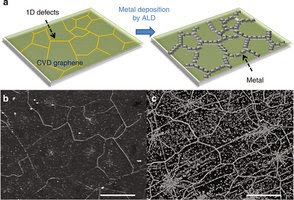
Developments in nanoelectronics and nanoscale surface modification have continued to drive the need for more elegant and reliable bottom-up area selective deposition (ASD) strategies. Most notably, the semiconductor industry has relentlessly pursued sub-10 nm transistor fabrication for next-generation devices, an endeavor that increasingly relies on selective deposition techniques to facilitate proper material alignment. However, other fields beyond traditional transistor fabrication have also found potential applications for selective deposition. Mixed-material catalysts have consistently shown the benefits of having site-specific material growth, but new optical devices and materials for energy storage have also contributed to an increased focus on developing new strategies for ASD.
Website: https://asd2020.avs.org/

The website for the 2020 Area Selective Deposition Workshop is now live! Come join us next April 2-3 at Stanford to learn about the cutting edge science being performed around the world! #Area_Selective #ASD20 #ALDep #CVDep https://t.co/MJxTgGECkf— Bent Group (@BentGroup) September 11, 2019
In an effort to help facilitate the progression of ASD techniques, Stanford University is proud to host the 5th Area Selective Deposition Workshop (ASD 2020), held on April 2–3, 2020 in Palo Alto, California USA. Located in the heart of Silicon Valley, this year’s workshop will act as a central event for sharing and discussing the newest developments in ASD by gathering leading experts from both academia and industry. Attendees can expect to participate in talks regarding fundamental challenges related to recent developments in ASD, applications for ASD in next-generation technology, emergent processes for implementing ASD techniques, and new perspectives on metrological and characterization strategies for further understanding persistent mechanistic challenges.
Based on the success of the previous workshops, ASD 2020 will consist of two days of presentations by invited and contributing speakers, as well as a banquet reception and poster session at Stanford University. We hope that guests will also have time to experience some of the local attractions and natural beauty that the Bay Area has to offer!


