


%20(1).png)
Here is an interview with Prabu Raja, group vice president, fellow at Applied Materials and general manager for the Patterning and Packaging Group at Applied Materials, by Mark Lapedus at Semiconductor Engineering.
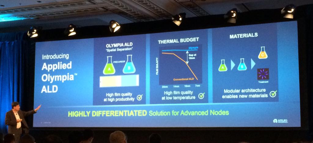
Prabu Raja, Group VP, Patterning & Packaging group, highlights Applied Materials Centris Sym3 Etch & Olympia ALD 2015 (Applied_Blog on Twitter)
The interview covers the upcoming hurdles like overlay and edge placement error in patterning at the 7 and 5 nm node and technologies to solve them:
- Extreme ultraviolet (EUV) lithography
- Self-aligned octuple patterning (SAOP)
- Atomic Layer Etching (ALE)
- Selective removal
- Atomic Layer Deposition (ALD)
- Selective deposition
Applied Materials Revolutionizes Etch with Breakthrough Selective Materials Technology https://t.co/MMsqJvEBgs pic.twitter.com/zbcrneqsgi— Applied Materials (@Applied_Blog) June 29, 2016
No comments:
Post a Comment