Friday, September 1, 2023
Unlocking MEMS Manufacturing Excellence: Dive into ALD's Potential!
SiC Market Soars Towards $9 Billion: EVs and High-Power Chargers Drive Growth
Strategic Shift to 8-Inch Wafers: Opportunities and Challenges Shape SiC's Next Phase
According to Yole, the Silicon Carbide (SiC) market is on a robust trajectory, poised to reach nearly $9 billion by 2028, driven by a dynamic blend of growth factors. The automotive sector, particularly Battery Electric Vehicles (BEVs) and 800V EV systems, spearheads this expansion. SiC's prominence extends to EV DC chargers, offering immense potential for high-power modular chargers. Additionally, SiC plays a pivotal role in energy supply, with installations expected to surge between 2022 and 2028. Industrial power supplies, motor drives, and rail systems further diversify SiC's applications. This Yole report underscores SiC's prowess in high-efficiency power electronics across industries, shaping a transformative market landscape.
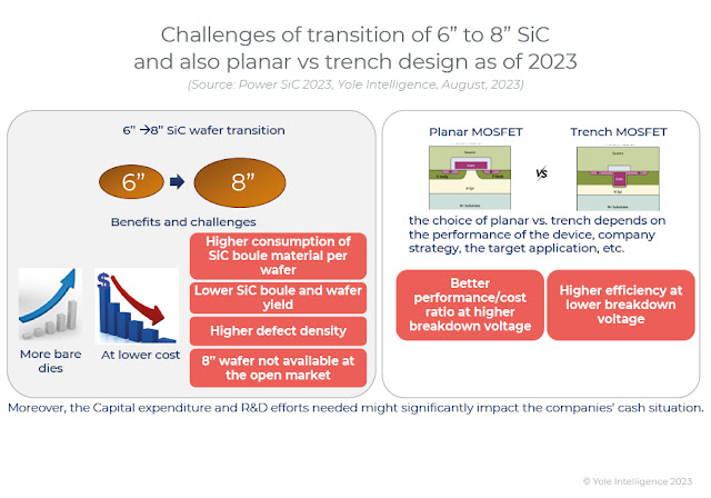
The report indicates that as of 2023, the mainstream SiC wafer size for leading players is still 6 inches. However, there are strategic discussions and plans surrounding the transition to 8-inch (200 mm) SiC wafers. While Wolfspeed is currently the only player producing SiC devices on the 8-inch platform, other companies have announced their intention to follow suit. The adoption of 8-inch wafers presents both opportunities and challenges.
Challenges associated with 8-inch wafer production include higher costs, longer equipment lead times, potentially lower initial yield rates due to the larger size, and concerns about the availability of these wafers. Wolfspeed's early adoption of 8-inch wafer production reflects their proactive stance in developing the technologies and processes required to overcome these challenges.
The transition to 8-inch wafers is an area of focus due to the potential advantages it offers, such as increased capacity and improved cost efficiency over time. However, the challenges mentioned earlier are critical factors that need to be addressed for a successful transition. Companies are investing in innovative approaches and strategies to ensure a smooth migration to the 8-inch platform, which has the potential to impact the SiC power devices market significantly in the coming years.
Yole Group - Follow the latest trend news in the Semiconductor Industry
Thursday, August 31, 2023
Metal Plating Chemicals Revenues to Boost into 2024
Growth driven by developments in leading-edge logic and memory
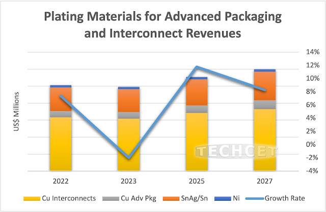
“Increased usage of advanced packaging, redistribution layers, and copper pillar structures are all factors contributing to the growth of the metal chemicals market segment,” states Dr. Karey Holland, Chief Strategist at TECHCET.
Balancing Fundamental and Applied ALD with Stacey Bent – ALD Stories Ep. 26
Wednesday, August 30, 2023
Announcement Symposium G01 on “ALD & ALE Applications, #19” at the 244th ECS Meeting in Gothenburg, Sweden, Oct. 8-12, 2023
Announcement Symposium G01 on “ALD
& ALE Applications, #19”
at the 244th ECS
Meeting in Gothenburg, Sweden, Oct. 8-12, 2023
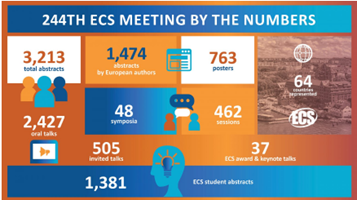
See for detailed information about the 48 symposia, late manuscript submission requirements, and financial assistance: https://www.electrochem.org/244/.
6K Energy Partners with Forge Nano to Revolutionize Battery Material Production
6K Energy, a trailblazer in sustainable battery material production, has joined forces with Forge Nano to introduce cutting-edge Atomic Layer Deposition (ALD) technology for commercial-scale production of NMC 811 cathodes. This collaboration aims to transform the battery industry by enhancing performance, efficiency, and cost-effectiveness.
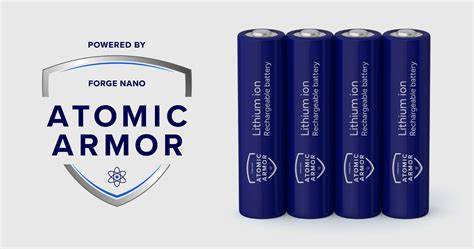
Forge Nano, known for its precision nano-coating technology, and 6K Energy are set to redefine battery material production. By integrating Forge Nano's proprietary Atomic Armor™ surface technology into 6K Energy's process, the partnership promises unparalleled advancements.
Atomic Armor employs ALD coatings with unprecedented precision and speed. This method enhances battery materials, resulting in superior capacity, safety, charging rates, and cost-efficiency. Combining Forge Nano's Atomic Armor with 6K Energy's innovative UniMelt® materials production process is expected to yield high-performance and cost-effective battery materials.
Dr. Richard Holman, Senior VP of Battery Products at 6K Energy, emphasizes the impact of the collaboration, stating, "Leveraging Forge Nano's Atomic Armor platform provides us with a coating technology that meets the stringent specifications of our lithium-ion battery materials."
6K Energy's mission to produce domestically sourced battery materials for electric vehicles and renewable energy is greatly amplified by this collaboration. As the demand for advanced battery technologies grows, strategic partnerships like this one are poised to drive sustainable and high-performance solutions.
About 6K:
6K is a sustainability-driven company offering innovative solutions across industries. Their UniMelt® microwave plasma production system transforms materials into groundbreaking products. The company's 6,000-degree philosophy signifies both the operational temperature of UniMelt and the sun's surface temperature. 6K Energy, a division focused on domestically sourced battery materials, accelerates the transition to electric vehicles and renewable energy.
For more information, visit www.6Kinc.com.
6K Energy to Implement Forge Nano Equipment for Commercial Production of NMC 811 - Forge Nano
Monday, August 28, 2023
The Future of Nanoimprint Lithography: Exploring Possibilities and Challenges for High-Volume Production
Nanoimprint lithography (NIL) has emerged as a promising technique for the replication of intricate nano-scale features, offering higher resolution and uniformity compared to traditional photolithography methods. As semiconductor technology advances towards smaller and more complex structures, NIL holds the potential to revolutionize high-volume production processes. In this blog post, we'll delve into the current status of nanoimprint lithography and the possibilities it presents for future high-volume productions, as well as the main issues and concerns that need to be addressed.
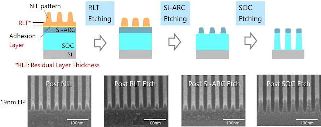
NIL utilizes a process where a patterned mask is brought into contact with a resist-coated substrate. The resist fills the relief patterns in the mask through capillary action, creating precise nano-scale features. With a focus on simplicity and cost-effectiveness, NIL doesn't require the complex optics found in traditional photolithography, making it an attractive option for semiconductor memory applications.
Early work on combining NIL and Atomic Layer Etching by AlixLabs Founders
Most Recent Achievements:
Recent study by TEL and Canon have demonstrated NIL's resolution capabilities of better than 10 nm, positioning the technology as a candidate for printing multiple generations of critical memory levels using a single mask. The potential to eliminate material waste by applying resist only where necessary adds to its appeal. Moreover, the simplicity and compactness of NIL equipment allow for clustered setups, enhancing productivity.
NIL Addressing Challenges in DRAM Scaling:
Dynamic Random Access Memory (DRAM) memory faces the challenge of continued scaling, with roadmap targets aiming at half pitches of 14 nm and beyond. The complexities of achieving tighter overlays, greater precision in critical dimensions, and edge placement errors demand innovative solutions. In DRAM fabrication, overlay requirements are even more stringent than in NAND Flash, with an error budget of 15-20% of the minimum half pitch.
Edge Placement Error (EPE):
EPE, the difference between intended and printed features, poses a significant challenge in modern semiconductor manufacturing. The intricacies of multiple patterning schemes and intricate device layouts contribute to EPE's complexity. Ensuring accurate placement of features is critical for maintaining device yield and performance.
The Quasi-Atomic Layer Etch (Quasi-ALE) process
The process is a specialized etching technique employed in advanced semiconductor manufacturing, particularly in processes like Nanoimprint Lithography (NIL). Quasi-ALE combines elements of Atomic Layer Etching (ALE) and conventional etching methods to achieve precise and controlled material removal. In the context of Nanoimprint Lithography, Quasi-ALE is used to etch materials with exceptional precision, targeting nanoscale features while minimizing damage to the surrounding areas. It involves a cyclic process where alternating etching and passivation steps are applied to the substrate. Each cycle removes a controlled layer of material, ensuring highly uniform etching and minimal lateral etch. One can discribe Quasi-ALE as a more productive way of performing ALE.
The key steps of the Quasi-ALE process typically involve:
1. Etch Step: During this step, a reactive gas is introduced into the etch chamber, which chemically reacts with the material to be removed. This reaction results in the selective removal of the material layer.
2. Passivation Step: In this step, a passivating species is introduced, forming a protective layer on the substrate surface. This layer prevents further etching and preserves the material beneath.
3. Purge and Repeat: The chamber is purged to remove any excess gases, and the process is repeated in a cyclical manner. Each cycle removes a controlled atomic layer of material.
Quasi-ALE is particularly advantageous for applications requiring high precision and control, such as in Nanoimprint Lithography, where maintaining accurate pattern dimensions and minimizing damage is critical. By combining the benefits of both ALE and traditional etching, Quasi-ALE enables advanced semiconductor manufacturing processes to achieve unprecedented levels of accuracy and uniformity.
Addressing EPE with Nanoimprint Lithography:
Researchers are actively exploring techniques to mitigate edge placement errors in nanoimprint lithography. This includes focusing on overlay accuracy, critical dimension uniformity (CDU), and local CDU. Compensatory methods such as dose control and reverse tone pattern transfer are being investigated to improve CDU and minimize errors.
The Role of Dose Control:
Varying the exposure dose offers a means of achieving small shifts in critical dimensions. Initial studies suggest that dose variations could lead to CD shifts of one to 2 nm. This strategy holds promise for enhancing CDU in the imprint process.
Reverse Tone Pattern Transfer:
Reverse tone processes, involving spin-on hard mask (SOHM) application and etch-back, offer an alternative approach to pattern transfer. While this method provides advantages such as reduced resist erosion and improved wall angles, trade-offs between CDU and line width roughness (LWR) need to be addressed.
Looking Ahead: The Possibilities and Challenges:
While NIL exhibits impressive potential, there are key challenges to overcome before it can be effectively integrated into high-volume semiconductor manufacturing. Ensuring precise overlay accuracy, managing complex CDU requirements, and effectively addressing edge placement errors remain pivotal. As the industry strives to achieve the roadmap's aggressive scaling targets, the evolution of nanoimprint lithography will undoubtedly play a crucial role.
Nanoimprint lithography is poised to reshape the semiconductor manufacturing landscape, offering higher resolution and cost-efficiency compared to traditional methods. With ongoing research and development, addressing challenges such as overlay accuracy, CDU, and EPE, the path to successful high-volume production through NIL seems promising. As technology continues to advance, the journey towards perfecting nanoimprint lithography is an exciting one, holding the potential to shape the future of chip fabrication.
Tokyo Electron (TEL):
TEL specializes in Nanoimprint Lithography (NIL) technology, offering precision equipment, advanced etching solutions, and expertise in process control. They excel in alignment, overlay correction, CDU management, and etching technology.
Canon:
Canon contributes to Nanoimprint Lithography (NIL) advancement by leveraging TEL's strengths in alignment, overlay correction, CDU management, and advanced etching solutions. They integrate these capabilities with the Reverse Tone Pattern Transfer, ensuring precise pattern replication and fidelity. Canon's focus on innovation drives high-resolution, cost-effective solutions for semiconductor manufacturing.
Canon has introduced a groundbreaking solution in the field of semiconductor technology with the development of the world's first mass-production equipment called the "FPA-1200NZ2C." This innovative tool utilizes nanoimprint lithography, a cutting-edge technique that involves imprinting nanometer-scale mask patterns onto substrates. By adopting this novel approach, Canon aims to overcome the limitations of conventional miniaturization methods. The FPA-1200NZ2C is already in use by Toshiba Memory, a prominent semiconductor memory manufacturer. This advancement marks a significant step forward in semiconductor manufacturing, enabling the creation of more intricate and advanced circuit patterns.
Sources:
High-Definition Nanoimprint Stamp Fabrication by Atomic Layer Etching — Lund University
Nanoimprint post processing techniques to address edge placement error (spiedigitallibrary.org)
Nanoimprint Lithography | Canon Global
FPD Lithography Equipment | Canon Global
Benefits of atomic-level processing by quasi-ALE and ALD technique - IOPscience
Acknowledgement :
Thanks for sharing the SPIE article on LinkedIn and giving insights Frederick Chen!
Sunday, August 27, 2023
The Industiral Ecosystem of Si Chips and Atomic Layer Deposition - Webinar
 https://brnw.ch/21wC0I4
 Dutch Scientists at TNO & TU Eindhoven Develop Efficient Monolithic Perovskite-PERC Tandem Solar Cell
Highlights
- •
Champion 23.7% efficient perovskite-PERC tandem cell was achieved.
- •
The developed thermal atomic layer deposition (ALD) process for NiO is reported.
- •
ALD NiO was added to an ITO/SAM recombination junction to improve the device yield.
Dutch researchers at TNO and TU Eindhoven have achieved a notable breakthrough in solar cell technology by creating a monolithic perovskite-PERC tandem solar cell with a remarkable 23.7% efficiency. The innovation lies in a new tunnel recombination junction (TRJ) design that includes indium tin oxide (ITO), carbazole (2PACz), and a nickel(II) oxide (NiO) layer. Unlike conventional TRJs, the addition of NiO significantly reduces electrical issues in the perovskite top cell.
(a) HAADF-scanning transmission electron microscopy (TEM) image of a tandem cell using ITO/NiO/2PACz. (b) Compositional line profiles at the interface ITO/NiO/SAM extracted from an EDX elemental mapping. Note that the figure is rotated 90°.
By using atomic layer deposition (ALD), the team improved the uniformity of the self-assembled monolayer (SAM) in the TRJ structure. This new solar cell design includes a perovskite absorber, electron transport layers, an ITO electrode, a silver (Ag) metal contact, and an antireflective coating.
Comparing their creation with a reference cell, the researchers found the novel TRJ-based cell achieved an efficiency of 23.7%, slightly below the reference cell's 24.2%. However, the novel design's uniform coverage of SAM and consistent efficiency across different devices within and between batches makes it promising for large-scale production.
Published in Solar Energy Materials and Solar Cells, this research opens doors for improved perovskite-PERC tandem solar cell technology using ALD NiO.
Atomic layer deposition of NiO applied in a monolithic perovskite/PERC tandem cell - ScienceDirect
Trelleborg Sealing Solutions Unveils State-of-the-Art Semiconductor Seals and Pioneering Engineering Expertise at Semicon Taiwan 2023: Spotlight on Atomic Layer Deposition Application
Trelleborg Sealing Solutions Exhibits Advanced Semiconductor Seals and Engineering Prowess at Semicon Taiwan 2023
Trelleborg Sealing Solutions, a leading player in engineering solutions, is making waves at Semicon Taiwan 2023 by showcasing its cutting-edge engineering capabilities and an expanded range of semiconductor sealing solutions. The event, hosted at the Taipei Nangang Exhibition Center, features Trelleborg's booth highlighting their latest additions to the Isolast PureFab FFKM material range, a significant advancement in semiconductor seal technology.
At the forefront of their display is the Isolast PureFab JPF40, an ultra-high temperature perfluoroelastomer (FFKM) designed for demanding subfab applications and thermal processes. This includes pivotal processes such as rapid thermal processing (RTP) and atomic layer deposition (ALD), crucial for semiconductor manufacturing. This material boasts unparalleled compression set performance within a wide operating temperature range, ensuring airtight seals in critical processes even at extreme temperatures reaching +300°C. The remarkable capability to withstand peak application temperatures exceeding +325°C makes it a game-changer in the semiconductor industry.
Ethan Huang, the Semiconductor Segment Manager at Trelleborg Sealing Solutions, emphasized the vital role of reliable sealing solutions in safeguarding semiconductor processes against escalating temperatures and aggressive chemical agents. The Isolast PureFab JPF40 and other offerings within the PureFab range are meticulously engineered to address the unique challenges posed by semiconductor environments.
Furthermore, Trelleborg's expertise extends to predictive engineering through finite element analysis. This innovative approach aids in modeling compression set data, allowing engineers to more accurately estimate the usable lifetime of seals during design and production. This predictive technology is a significant leap forward, enabling enhanced seal longevity assessments.
A standout in their exhibition is the Isolast K-Fab Flange Seal, designed for critical subfab applications and capable of withstanding temperatures up to +327°C, dependent on material selection. The seal's versatility in material options, including Isolast FFKM, PureFab FFKM, and PureFab Fluoroelastomer (FKM), makes it adaptable to various requirements.
An interesting focus lies on Trelleborg's contributions to atomic layer deposition (ALD). Their materials, like Isolast PureFab JPF22, exhibit remarkable chemical compatibility with wet process chemicals, steam, and amine-based ALD precursors. This makes them well-suited for ALD applications, which are vital to modern semiconductor fabrication processes.
In addition to their product lineup, Trelleborg also presents the Turcon Variseal NW, showcasing their prowess in spring-energized seals for extreme environments. This seal operates across an extensive temperature range and excels in both wear resistance and friction characteristics.
Semicon Taiwan 2023 provides a platform for Trelleborg Sealing Solutions to not only showcase their groundbreaking products but also to engage with industry professionals about their specific sealing needs. The event highlights the convergence of innovative engineering and the semiconductor industry's evolving demands.
Saturday, August 26, 2023
SK Hynix Leads DRAM Industry's Rebound in Q2 with Revenue Surge, Reclaims No. 2 Position
South Korea's SK Hynix Inc. has orchestrated a substantial resurgence in the DRAM chip sector during Q2, propelling itself back to the second-largest global position and surging ahead of Micron Technology Inc., which now stands third. The chipmaker achieved a nearly 50% surge in DRAM shipments, propelling its revenue to $3.44 billion in the April-June period. Notably, SK Hynix excelled in DDR5 and HBM chip shipments, products with higher average selling prices (ASPs) than standard commodity DRAM items, thus enhancing its ASP growth by 7-9% compared to the previous quarter. In contrast, market leader Samsung Electronics experienced a 7-9% ASP drop while retaining its top position, and third-place Micron sustained relatively stable ASP with DDR5 shipments. The overall DRAM industry marked a 20.4% QoQ revenue increase in Q2, signaling a potential turnaround in the sector.
SK Hynix leads DRAM industry’s Q2 revenue rebound, retakes No. 2 spot - KED Global
Global Semiconductor Industry Poised for 2024 Recovery Amidst Near-Term Challenges, SEMI Reports
In a recent report by SEMI, in collaboration with TechInsights, the global semiconductor industry shows signs of emerging from its downcycle, with a projected recovery expected in 2024. The report highlights that the third quarter of 2023 is anticipated to witness a healthy 10% quarter-on-quarter growth in electronics sales, while memory IC sales are set to achieve double-digit growth for the first time since the downturn began in 2022. Although headwinds persist in the semiconductor manufacturing sector during the latter half of 2023, a rebound is on the horizon.
Inventory drawdowns at integrated device manufacturer (IDM) and fabless companies are forecasted to keep fab utilization rates lower than those seen in the first half of 2023. Despite this, positive trends are noted in capital equipment billings and silicon shipments, stemming from government incentives and robust equipment sales backlogs.
Market indicators suggest the semiconductor industry reached its nadir by mid-2023, commencing a path to recovery, setting the stage for growth in 2024. All segments are predicted to witness year-over-year increases in 2024, with electronics sales projected to surpass their 2022 peak.
Clark Tseng, Senior Director of Market Intelligence at SEMI, pointed out that the gradual demand recovery might extend the timeline for inventory normalization until the end of 2023, leading to temporary reductions in fab utilization rates. Nevertheless, semiconductor manufacturing is expected to hit its bottom in Q1 2024.
Boris Metodiev, Director of Market Analysis at TechInsights, highlighted the resilience of equipment sales and fab construction despite the broader downturn. He attributed this trend to government incentives driving new fab projects and strong backlogs supporting equipment sales.
Original Source: SEMI https://www.semi.org/en/news-resources/press-releases/2023/08/global-semiconductor-industry-on-track-for-2024-recovery-but-near-term-headwinds-remain-semi-reports
Friday, August 25, 2023
AI Chip Market Poised to Soar: Gartner Predicts Revenue to Reach $53 Billion in 2023, Double by 2027
TRION Battery and Forge Nano Partner to Advance Lithium-Ion Battery ALD Tech
German Firm EMD Electronics Invests $300 Million to Expand Semiconductor Manufacturing in Pennsylvania
Germany-Based EMD Electronics Expands Schuylkill County, Pennsylvania, Operations - Area Development EMD Electronics, the North American electronics business of Merck KGaA, plans to expand its operation and establish a semiconductor specialty gasses manufacturing facility in Schuylkill County, Pennsylvania. The $300 million project is expected to cr www.areadevelopment.com |
Thursday, August 24, 2023
Global Semiconductor Market Trends & Electronic Gases: USA, China, Europe, and Beyond
Innovating Coating Technologies: A Spotlight on Swiss Cluster's Advanced ALD Products
In the dynamic landscape of materials science and technology, Swiss Cluster emerges as a pioneering force with its cutting-edge Atomic Layer Deposition (ALD) solutions. Founded by a team of experts hailing from the Swiss Federal Institute for Material Science & Technology (Empa) in Thun and Bern University of Applied Sciences, Swiss Cluster has swiftly carved a niche for itself in the field. The company's commitment to innovation and precision is evident in its diverse range of ALD products, each tailored to meet the demands of various industries and applications.
Swiss Cluster's journey began in 2019, and it officially registered as a company in November 2020. The driving force behind Swiss Cluster's success lies in the collective expertise of its team, which encompasses researchers and engineers specializing in thin films deposition techniques, vacuum and plasma deposition technologies, and materials characterization. This robust foundation has paved the way for the creation of three exceptional ALD products that are reshaping the way coatings are applied to 3D objects.
1. SC Optima Series: Elevating Coating Precision and Efficiency
The SC Optima Series stands as a testament to Swiss Cluster's commitment to innovation and efficiency. Designed as the next generation of large batch systems for ALD, this series embodies the perfect synergy of precision, speed, and uniformity. Boasting a patent-pending chamber, the SC Optima Series can seamlessly adapt to various 3D parts and coating materials. Its exceptional coating homogeneity and record process speeds are achieved through the elimination of traditional barriers like transfer arms, thanks to the single chamber approach. This innovation not only streamlines loading and unloading but also facilitates rapid temperature control, optimizing the entire process from start to finish.
2. SC-1: Redefining Coating Systems with Integration
The SC-1 redefines what's possible in coating technologies by combining ALD with Physical Vapor Deposition (PVD). This groundbreaking modular system eliminates the need for vacuum breaks, minimizing downtime and maximizing throughput. The SC-1's ability to seamlessly integrate ALD and PVD techniques within a compact framework allows for the fabrication of multinanolayered coatings. This approach improves coating quality, stability, and material properties, making it a powerful tool for industries requiring tailored functionalities and properties. The SC-1's flexibility, scalability, and quality interfaces between different layers open doors to novel materials and applications.
3. SC Qube: Precision for Research and Production
For those focused on research, development, and small-scale production, the SC Qube offers an innovative solution. With its ALD batch system, the SC Qube caters to coating various 3D parts. The system's scalable chamber can be configured to fit different types and sizes of objects while delivering exceptional coating homogeneity. The ability to integrate the SC Qube into cleanroom environments or glovebox units, along with its easy front loading and custom-made holders, makes it a versatile choice for various applications. Rapid processing, precision, and adaptability define the SC Qube's contribution to the world of coatings.
Swiss Cluster's trio of ALD products represents a journey of expertise, innovation, and a commitment to enhancing the way materials are coated. From large batch systems to integrated solutions and research-focused offerings, Swiss Cluster's ALD products cater to the unique needs of different industries. As the company continues to push boundaries and refine coating technologies, its impact on diverse sectors, from electronics to medical applications, remains profound. Swiss Cluster's dedication to revolutionizing research and production processes paves the way for novel and better materials that shape our technological future.
TSMC Marks Major Milestone: First EUV Machine Installed in Arizona Fab, Job Opportunities Open
Taiwan Semiconductor Manufacturing Co. (TSMC) has achieved a significant milestone in its Arizona manufacturing venture by installing its inaugural extreme ultraviolet lithography (EUV) machine. This advanced machine, procured from Dutch semiconductor equipment leader ASML Holding NV, is a pivotal asset for TSMC's future high-end chip production endeavors.
EUV technology is a critical aspect of semiconductor fabrication, facilitating the printing of intricate designs on microchips significantly smaller than a human hair. TSMC's achievement underscores its commitment to innovation and technological leadership.
While the installation of the EUV machine marks a remarkable accomplishment, TSMC acknowledges that the setup of the new fab in Arizona involves numerous additional tasks. The company emphasized the need for approximately 2,000 skilled workers to handle the installation of various equipment pieces and services in the complex. This requirement stems from TSMC's unique tool configurations and specifications.
TSMC, recognized as the world's largest contract chip manufacturer, is channeling substantial investments amounting to $40 billion into constructing two wafer fabs in Phoenix. The first facility will employ the advanced 4-nanometer process, while the second, already under construction, will utilize the more sophisticated 3-nanometer process. This latter technology has already entered mass production in Taiwan.
The presence of skilled workers has been a contentious topic linked to the Arizona project. TSMC Chairman Mark Liu explained that a deficiency in experts capable of properly installing equipment at the Arizona site has led to a delay in mass production, now projected for 2025 rather than late 2024.
However, TSMC's approach to addressing this shortfall has sparked debates. The company's bid to bring in around 500 Taiwanese workers on temporary E-2 visas has faced resistance from local unions, who assert that prioritizing American jobs is paramount, especially considering the significant subsidies TSMC seeks under the CHIPS and Science Act. This legislation, signed by President Joe Biden, encourages semiconductor investments in the United States.
US Senator Mark Kelly of Arizona emphasized that the visa applications will be evaluated in accordance with established laws and procedures. As TSMC navigates these challenges, its progress in Arizona remains a focal point in the semiconductor industry's dynamic landscape.
TSMC installs first EUV machine in U.S.; job opening ads posted - Focus Taiwan


%20(1).png)

