Monday, November 23, 2015

Disruptive atomic level particle free metallic ink products

I was, as usual, searching for any news about ALD and came across this press release from Liquid X. Funny that anything on atomic level can be regarded as disruptive these days - and yes I am proud of the headline, which originally red "ALD - More than 41 years of descriptiveness"


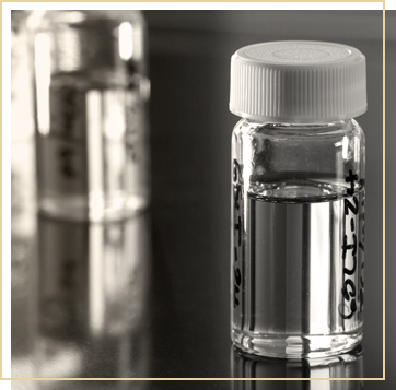
"Liquid X Printed Metals®, Inc. is a technology company headquartered in Pittsburgh, Pennsylvania that manufactures functional metallic inks. Liquid X® inks are considered disruptive in that their technology is on the atomic level. This provides processing advantages and achieves better metal film properties than other metallic inks that feature nanoparticles and metal flakes."

Liquid X Printed Metals® Introduces Particle-free Products

Formulated at the Atomic Level, Two Disruptive Metallic Ink Products are Thin, Robust, Adaptable and Cost-effective


PITTSBURGH - Liquid X Printed Metals ®, Inc., (Liquid X®), an advanced material manufacturer of functional metallic inks, today introduced two particle-free inks.  The inks will enable manufacturers in the electronics and other industries to produce thinner, more cost-effective and adaptable electronic components that will drive innovation in consumer electronics, and advanced and medical technology among other industries.

The company's two inaugural products, Liquid X®'s Silver Inkjet Ink and Silver Flexo Ink were developed using an original and proprietary particle-free formulation that leads to more cost-effective and trouble-free processing; more durable traces that withstand bending and flexing; adherence to the full range of substrates; good conductivity; excellent printability; and enhanced sustainability due to its water-based composition.

"Liquid X® is introducing particle-free inks that eliminate problems associated with other metallic inks that are made with less stable nanoparticles or metal flakes, which are thicker and can cause clogging, slowness and other problems in printing," said Greg Babe, President and CEO of Liquid X®.  "Our Silver Inkjet Ink and Silver Flexo Ink leverage atomic-level technology, which represents the kind of powerful, robust and adaptable innovation required to tap the fullest potential of printed electronics."

Liquid X(®)'s molecular inks consist of novel metal complexes that are printed as solutions that are used in the creation of films or traces that exhibit high conductivity, are thin and precise, and allow for low-temperature processing that enables adherence on a wide range of substrates. And the low viscosity of the inks allow for use in printing methods that include inkjet, aerosol jet, flexography, and gravure.

Liquid X(®)'s conductive inks are designed for applications that range from transparent conductors and touchscreens, to photovoltaic, industrial and automotive applications, and smart packaging.

Performance


Silver Inkjet Ink features viscosity at 6-9 cPs; Polar Protic Solvents; thermal, photonic and infrared curing methods; adherence to all substrates; and excellent stability when refrigerated. Film trace sheet resistance for one layer is 0.5 - 1 ohms per square.  Thickness for one layer is 200-300 nm.  Trace width is < 50 micrometers.  (Adhesion, tensile - ASTM D3359, 5B rating).  (Adhesion shear - scrub resistant.)  [Gloss - ASTM D523 ISO 2813, At 60 degrees >70 Gloss Units (high gloss)

Silver Flexo Ink features Flexo-Gravure deposition; viscosity at 110-140 cPs (1-50 RPM); 80-110 (60-100 RPM); ~25 sec #2 Zahn Cup;  Polar Protic Solvents; thermal, photonic and infrared curing methods; adherence to all substrates; and excellent stability at room temperature or when refrigerated. Film trace sheet resistance for one layer is 0.5 - 1 ohms per square.  Thickness is 1-3 microns.  (dependent on anilox).   (Adhesion, tensile - ASTM D3359, 5B rating).  (Adhesion shear - scrub resistant.)  [Gloss - ASTM D523 ISO 2813, At 60 degrees >70 Gloss Units (high gloss)

In development is a product called Silver Stretchable Ink, which is designed for stretchable substrates such as fabrics or elastomers.  Applications for Silver Stretchable Ink include wearables, soft robotics and other customized applications.

About Liquid X

Liquid X Printed Metals®, Inc. is a technology company headquartered Pittsburgh, Pennsylvania that manufactures functional metallic inks. The company's inks are considered disruptive in that their technology is on the atomic level. This provides processing advantages and achieves better metal film properties than other metallic inks that feature nanoparticles and metal flakes which create instabilities. Visit: www.liquid-x.com.

Sunday, November 22, 2015

SK Hynix & SNU demonstrate 28nm RRAM cell with ultra thin ALD Ta/Ta2O5 stack

Here is a impressive report by SK Hynix & Prof. Hwang and co-workers SNU on a RRAM device with Ta/Ta2O5 stacked RS layers with ultra-thin Ta2O5 thicknesses (0.5–2.0 nm) deposited by ALD. Woah that´s thin  - like the same order of thickness like native oxide, which makes me wonder if teh extra couple of ALD cycles was needed --> I need to study the paper more carefully!

Thickness effect of ultra-thin Ta2O5 resistance switching layer in 28 nm-diameter memory cell 

C.S. Hwang et al

Scientific Reports 5, Article number: 15965 (2015)
doi:10.1038/srep15965
(a) Schematic diagram and (b) TEM image of the TiN/Ta2O5/Ta/TaN device. Ta2O5 (0.5 nm) device, and (d) Ta2O5 (1.5 nm) device. Insets show the linear I-V plot. Scanning transmission electron microscopy (STEM) high angle annular dark field (HAADF) images of (c) 0.5 nm-thick device and (d) 2.0nm-thick device. 

Resistance switching (RS) devices with ultra-thin Ta2O5 switching layer (0.5–2.0 nm) with a cell diameter of 28 nm were fabricated. The performance of the devices was tested by voltage-driven current—voltage (I-V) sweep and closed-loop pulse switching (CLPS) tests. A Ta layer was placed beneath the Ta2O5 switching layer to act as an oxygen vacancy reservoir. The device with the smallest Ta2O5 thickness (0.5 nm) showed normal switching properties with gradual change in resistance in I-V sweep or CLPS and high reliability. By contrast, other devices with higher Ta2O5 thickness (1.0–2.0 nm) showed abrupt switching with several abnormal behaviours, degraded resistance distribution, especially in high resistance state, and much lower reliability performance. A single conical or hour-glass shaped double conical conducting filament shape was conceived to explain these behavioural differences that depended on the Ta2O5 switching layer thickness. Loss of oxygen via lateral diffusion to the encapsulating Si3N4/SiO2 layer was suggested as the main degradation mechanism for reliability, and a method to improve reliability was also proposed.


The web page for the joint EuroCVD-BalticALD 2017 in Sweden is up!

The web page for the joint EuroCVD-BalticALD 2017 in Sweden is up!

Check it out here : eurocvd-balticald2017.se


ALD Systems Guide at AZO Nano is updated

ALD Systems Guide at AZO Nano is updated - if you´re planning to invest in some new ALD equipment - check it out!

AZO Nano ALD Guide: http://www.azonano.com/nanotechnology-equipment.aspx?cat=33

 
The collection is not complete but a good start. Interesting is that there is still an offering for Aviza Technology Celsior fxP Single Wafer ALD System that used to run The famous NOLA Process on for 90 and 70 nm Deep Trench DRAM Production at Infineon / Qimonda, Nanya, Inotera, and Winbond. Probably not active anymore.

Friday, November 20, 2015

Guest Blog: ALD Russia 2015 workshop: travel notes by Riikka P...


Below you find my travel report from the ALD Russia workshop in Dolgoprudny, Moscow region, September 2015. Originally, this travel report was published as a stand-along text through Google docs and also through through BALD Engineering blog


After the ALD Russia workshop, this ALD History blog has been created, and one travel report published in it (St. Petersburg, 2015, Puurunen). Since the ALD Russia workshop was historical in nature in many ways, and since it will be wise to collect ALD-history-related travel reports in one place, I want to publish the travel report here again. To this version, I have added a significant number of previously unpublished photographic material. 

Can ALD save Moore´s Law?

Can ALD save Moore´s Law? - I would say it already did at the introduction og HKMG and some other things. Here is a great peace by Mark Lapedus with some insights from the leading extperts of industry and academia and I selected to high light some of them below:

Can Nano-Patterning Save Moore’s Law?

Selective deposition is showing promise in the lab, but it’s a long way from there to production.

For years the academic community has explored a novel technology called selective deposition. Then, more than a year ago, Intel spearheaded an effort to bring the technology from the lab to the fab at 7nm or 5nm. Today, selective deposition is still in R&D, but it is gaining momentum in the industry.


 “In order to make ALD-enabled nano-patterning available in the semiconductor industry, careful ALD precursor and reactant selections are required,” Samsung’s Han Jin Lim said.  


“There are a couple of places where selective deposition has been done in the past. But the applications have been pretty specific, where we have gotten our arms around the defectivity issues,” said Dave Hemker, senior vice president and chief technology officer at Lam Research. “But anytime you go selective and deposition, you’ve have to make sure the defectivity and other issues are solved. As we learn more about it, we’ll see more applications coming out of it.”


“With SAM, it might be possible to do selective-area ALD or CVD by area-deactivation,” said Erwin Kessels, a professor at the Eindhoven University of Technology. “But this only provides a solution in cases where the substrate is already patterned. Selective deposition by area-deactivation doesn’t really help you in most cases when you really want to generate patterns from the bottom-up, which is the ultimate aim. Yet, it would still be helpful to reduce the number of litho steps.”

Continue reading : http://semiengineering.com/can-nano-patterning-save-moores-law/ 

Liquid ALD by Self-terminated electrodeposition of iridium electrocatalysts

Here is an interesting report on liquid ALD from NIST covered by Nanowerk News: "Remember that pair of gold electroplated earrings you bought years ago at the mall? Key to crafting their allure was the ability to place an ever-so-thin layer of valuable metal atop a less costly base material. This same strategy will be central to building the “engines” of future hydrogen-powered cars, and scientists at the National Institute of Standards and Technology (NIST) have developed a way to do it more effectively with metals rarer than gold ("Self-terminated electrodeposition of iridium electrocatalysts")."


Gray center section shows individual atomic layers of iridium NIST scientists deposited, one layer at a time, atop a base of gold, with the boundary between the two metals clarified by the green/red image at right. A top view is shown at left in gold. The deposition technique, which also works with other important metals, could produce economical catalysts for hydrogen fuel cells and water electrolysis. (Picture and text from Nanowerk)

Self-terminated electrodeposition of iridium electrocatalysts


Sang Hyun Ahn,   Haiyan Tan,   Mareike Haensch,   Yihua Liu,   Leonid A. Bendersky and   Thomas P. Moffat.
Energy Environ. Sci., 2015, Advance Article
DOI: 10.1039/C5EE02541A

A simple electrochemical process for submonolayer deposition of ultrathin catalytic Ir films is demonstrated. This method enables effective utilization of one of nature's rarest elements while different substrates facilitate the exploration of promising bimetallic catalysts for a sustainable hydrogen economy. Semi-coherent Ir films were deposited on Au, Pt and Ni substrates using K3IrCl6–Na2SO4–H2SO4 electrolytes operated between 40 °C and 70 °C. However, the deposition reaction is quenched at the onset of H2 production where adsorbed H blocks the reduction of IrCl6−xH2Oxx−3 to Ir. The electrode can be reactivated for further deposition by pulsing the potential to more positive values where adsorbed H is oxidized. The electrocatalytic activity of ultrathin Ir and Pt films, and combinations thereof, were examined as function of the number of self-terminating deposition pulses. The ultrathin films match or exceed the best reported activity metrics for hydrogen oxidation in alkaline media and oxygen evolution in acid.

Wednesday, November 18, 2015

Graphene - ALD bendable Supercaps by Nanyang Technological University and Partners

Nanowerk had an interesting post today on how Nanyang Technological University and Partners in Singapore and China are using graphene and ALD Metal Nitrides to fabricate bendable solid-state asymmetric super capacitors. Check out the processing to achieve the metal nitrides below - not the usual way but via the oxides and solution based chemistry! I assume that graphene is a tricky material to grow metal nitrides on


Illustration of the asymmetric supercapacitor, consisting of vertically aligned graphene nanosheets coated with iron nitride and titanium nitride as the anode and cathode, respectively. (as published in Nanowerk, ©WILEY-VCH Verlag)


"To get the maximum benefit from the graphene surface, the team used a precise method for creating thin-films, a process known as atomic layer deposition, to grow two different materials on vertically aligned graphene nanosheets: titanium nitride for their supercapacitor’s cathode and iron nitride for the anode." 


Tracking back to the original publication in Advanced Materials "All Metal Nitrides Solid-State Asymmetric Supercapacitors" DOI: 10.1002/adma.201501838 there are some more details available in the free to download supporting information from the authors where it is reviled that a BENEQ TFS 200 ALD reactor was used for the cathode and anode. Here´s the link and some details are given below:

A BENEQ TFS 200 that come in many sorts and flavours (www.beneq.com)

Electrode Material Synthesis

Preparation of TiN@GNS Cathode: All chemicals were bought from Sigma Aldrich and used without further purification. Graphene nanosheets (467 m2 g-1) were provided by INCUBATION ALLIANCE, INC. The cathode fabrication process is mainly composed of two steps: TiO2 deposition by atomic layer deposition (ALD) and transferring to nitride through annealing in ammonia (NH3) atmosphere. Before ALD, the GNS substrates were treated with oxygen plasma at 200 W for 10 minutes with an O2 gas flow of 100 sccm, 70 mTorr. In a typical ALD (Beneq TFS 200) process, 120 °C was applied to the GNS substrate with TiCl4 and water as the titanium and oxygen source, respectively. 166 cycles (~ 1.2 Å per cycle) deposition was conducted to obtain 20 nm TiO2 coating during which the reaction chamber was maintained with a steady N2 steam at 300 sccm (cubic centimeter per minute) at 1.0 mbar. The sample of TiO2@GNS was then annealed in NH3 atmosphere at 800 °C for 1 h with a gas flow of 50 sccm and heating rate of 20 °C per minute. The control sample of TiO2@GNS was synthesized with the same ALD process. 

Preparation of Fe2N@GNS Anode: 20 nm ZnO was deposited on GNS (oxygen plasma pretreated) with ALD at 200 °C. The ZnO@GNS sample was then immersed in 0.5 M Fe(NO3)3 solution for 2 h to have a thorough transformation from ZnO to FeOOH as reported by the previous work[1]. The FeOOH@GNS sample was then annealed with the same NH3 atmosphere situation at a lower temperature of 600 °C. The control sample of FeOOH@GNS was fabricated by the same method just without the afterward annealing.

Also Available in the supporting information linked above is a quite impressive results from a bending test odf a charged super capacitor (see figure below)


Capacitance retention of the full device at different bending conditions. "All Metal Nitrides Solid-State Asymmetric Supercapacitors" DOI: 10.1002/adma.201501838 (©WILEY-VCH Verlag).

Imec on taking 2D materials from lab to fab, and to technology

I just found this interesting article in Solid State Technology (abstract below) and realized again that 2D materials is actually steaming ahead and wafer level processing is happening today. Maybe 2D materials are to some extent even more promising than III/V channel integration on silicon wafers through horizontal or vertical Nanowires. One huge advantage as I see it is the lower thermal budget required for 2D Material growth or transfer processes which opens up huge possibilities for 3D stacking and continued scaling similar to what is happening for 3DNAND today.

Taking 2D materials from lab to fab, and to technology [Solid State Technology]

Due to their exciting properties, 2D crystals like graphene and transition metal dichalcogenides promise to become the material of the future.

BY STEFAN DE GENDT, CEDRIC HUYGHEBAERT, IULIANA RADU and AARON THEAN, imec, Leuven, Belgium.


The Technology roadmap as presented recently by Imec at the EWMOVPE workshop in Lund, Sweden, showing 2D materials as an option for beyond the 5 nm node.

As we enter into the era of functional scaling where the cross-roads of More-Moore and More-Than-Moore meet, the search for new devices and their enabling material comes to the forefront of technology research. 2D crystals provide very interesting form-factors with respect to traditional 3D crystals (bulk, Si, and III-V semiconductors). In this elegant 2D form, electronic structure, mechanical flexibility, defect formation, and electronic and optical sensitivity become dramatically different. Aaron Thean: “As researchers at imec explore the physics and applications of such material, it is now becoming important to find a wafer-scale path towards technology implementation and integration of these novel materials.” Working closely with research teams across universities and industry partners, the first important step for imec is to enable the flake-to-wafer transition, while concurrently exploring the material, and device-to-circuit applications. The work will build new infrastructure (e.g. epitaxy, metrology, patterning, and electrical characterizations, etc.) around it.

Continue reading in Solid State Technology

Interesting here is that imec is working on wafer level growth of MX2 materials "by a direct sulfurization process or by atomic layer deposition in the 200 and 300mm imec fabs.” This is not the first time that imec makes presentations in this area. I myself visited two events this year where imec presented work in this field - EWMOVPE workshop, Lund Sweden (above) and SEMICON Europa in Dresden (below).


Monolayer controlled deposition of 2D transition metal dichalcogenides on large area substrates, Presented by Annelies Delabie, Imec at SEMICON Europa 6th of October 2015, in Dresden.

I also visited SEMICON Europa 2014 where imec hosted a session on 2D Materials : http://www.semiconeuropa.org/node/2786 which was very interesting. However, there are probably some years of development ahead as ITRS has 5 nm introduction in the year 2020 or 2021 ready for mass production and that node will as we know it today not employ 2D materials.

Tuesday, November 17, 2015

CVD Equipment Corporation Revenue Rose 20.1% to Record-breaking Levels

It is soon Christmas so I think we ALD guys can be nice to the CVD guys. Some brief news from the world of CVD: CVD Equipment Corporation announced that it has achieved record-breaking revenue for both the three and nine month periods ended September 30, 2015. CVD’s revenue rose 20.1% to a record-breaking level of $10.6 million for the current quarter ending September 30, 2015 compared to $8.9 million in revenue for the quarter ended September 30, 2014. For the current nine month period, CVD’s revenue rose 59.0% to a record-breaking $30.8 million compared to $19.4 million in revenue for the nine month period ended September 30, 2014.  CVD also reported net earnings of $0.8 million or $0.13 per basic and diluted share and $2.8 million or $0.46 per share basic and $0.45 per share diluted for those respective periods compared to earnings of $0.9 million or $0.14 per share basic and diluted and $0.8 million or $0.13 per share basic and diluted for the three and nine months ended September 30, 2014


Full report: http://www.cvdequipment.com/2015/11/16/cvd-revenue-rose-20-1-to-record-breaking-levels/

Joiking aside,  CVD Equipment Corporation actually have an ALD Product offering. I do not know too much about this and here is the generic information that is available through their web:

Atomic layer deposition (ALD) is a thin film deposition process that allows for atomic layer thickness resolution, excellent conformity of high aspect ratio surfaces, and pinhole-free layers. This is achieved by sequential formation of atomic layers in a self-limiting reaction.


ALD is commonly used in the semiconductor industry for high-k dielectric films in CMOS processing, memory devices, MEMS, and sensors. The atomic layer deposition system is used for development of protective / functional coatings in fuel cells and other applications for corrosion / wear resistance. It can also be used to coat high aspect ratio structures like nanowires and nanotubes for next generation device development.

Oxides: Al2O3, TiO2, SnO, HfO2, ZnO, Fe2O3
Nitrides: TiN, TaN, WN
Metals: Cu, Ru, Ir, W and more.

Monday, November 16, 2015

BENEQ launches fast large area Spatial ALD

Following some of the other ALD companies (e.g. Veeco, SoLayTec, Levitech, Lotus, ALD NanoSolutions) BENEQ announced last Friday on their new Blog the coming of new spatial ALD equipment that is now going in to piloting. They will be sharing more information about the pilot runs with their new spatial ALD equipment later in through their blog : http://www.beneq.com/blog/201511/fast-large-area-spatial-ald-here.html


"The result is a revolutionary spatial ALD solution that takes the whole concept of continuous ALD to the next level, with processing scale and throughputs that have not been possible before. The ALD process now is like an automated car-wash, where the substrates move on a production line and each phase of the treatment is applied on the move. Based on the first results, it looks like we will completely redefine what high speed in ALD manufacturing means."

BENEQ Blog - A billion seconds - Stories from the home of ALD

Existing news and defenitely something forother ALD companies to follow - BENEQ Blog - A billion seconds - Stories from the home of ALD! This summer I had a chance to visit BENEQ and I was very much surpised by the size of their factory in Espoo, Finland - it is huge and it is all about ALD!


When you visit our factory in Espoo and enter the clean room area where we keep our 40 ALD machines, one thing you will notice is the constant ticking sound from the conventional batch ALD equipment. Those are the pulses of precursor gases in the equipment chambers ticking. Tick. Tick. Tick.

Combined with the humming background noise of the ventilation system and the vacuum pumps, it is a rather relaxing sound. It is one of the very characteristics that define the atmosphere of the factory floor.


ALD History Blog: Travel notes, St Petersburg, November 2015, by Rii...

ALD History Blog: Travel notes, St Petersburg, November 2015, by Rii...: I had the pleasure of visiting St. Petersburg in November 2015. This was my second visit to St. Petersburg related to ALD; the first was in ...

Prof. Drozd and his current design of thin film ALD reactor, at St Petersburg State University, made with the Nanoengineering brand. Photo by Riikka Puurunen, 11.11.2015.

Wednesday, November 11, 2015

Prof. Erwin Kessels TU Eindoven is appointed Associate Editor of the JVSTA

Professor W.M.M. (Erwin) Kessels of Eindhoven University of Technology Department of Applied Physics is appointed as an Associate Editor of the Journal of Vacuum Science & Technology(JVSTA). JVSTA has become a very important journal for ALD since it runs a special ALD issue after each International ALD conference. Here is a link to the upcoming issue : http://scitation.aip.org/upload/AVS/JVA/JVST_Special_Issue.pdf
 
 
Congratulations Erwin!

Biography

Erwin Kessels is a full professor at the Department of Applied Physics of the Eindhoven University of Technology TU/e (The Netherlands). He is also the scientific director of the NanoLab@TU/e facilities which provides open-access clean room infrastructure for R&D in nanotechnology. Erwin received his M.Sc. and Ph.D. degree (with highest honors) in Applied Physics from the TU/e in 1996 and 2000, respectively. His doctoral thesis work was partly carried out at the University of California Santa Barbara and as a postdoc he was affiliated to the Colorado State University and Philipps University in Marburg (Germany). In 2007 the American Vacuum Society awarded him the Peter Mark Memorial Award for "pioneering work in the application and development of in situ plasma and surface diagnostics to achieve a molecular understanding of thin film growth". From the Netherlands Organization of Scientific Research, he received a grant in 2010 to set up a large research program on "nanomanufacturing" in order to bridge the gap between nanoscience/nanotechnology and industrial application. His research interests cover the field of synthesis of ultrathin films and nanostructures using methods such as (plasma-enhanced) chemical vapor deposition (CVD) and atomic layer deposition (ALD) for a wide variety of applications, mostly within nanoelectronics and photovoltaics. Within the field of ALD, he has contributed to the field most prominently by his work on plasma-assisted ALD and his research related to ALD for photovoltaics. Erwinchaired the International Conference on Atomic Layer Deposition in 2008 and he has published over 200 papers and holds 2 patents.

Tuesday, November 10, 2015

Photo show: Workshop Simulation of chemistry-driven growth phenomena for metastable materials

CECAM/Psi-k/HERALD Workshop
Simulation of chemistry-driven growth phenomena for metastable materials


The controlled growth of thin films based on metastable materials by chemistry-driven processes is of high technological importance for topics like semiconductor devices or optical coatings. Computational modelling of this inherently multiscale process is crucial for an atomistic understanding and enables a decoupling and separate optimization of the growth-determining factors of non-equilibrium materials. This workshop will result in a joint effort by experts from different modelling communities covering the necessary length and time scales.

nearby Marburg in Germany from November 08-11, 2015.
 

Organizers

CECAMPsi-kHERALD
 

Photo Show


Awesome talk by Erwin Kessels on the ALD insight available by sum-frequency generation (Twitter, Henrik Pedersen)


Very good talk by @Simon_D_Elliott  pointing out the danger of using too simplified models for ALD (Twitter, Henrik Pedersen)

 
The Twitter master himself: Henrik Pedersen alias @hacp81 giving an invited on CVD (Twittter, Erwin Kessels)

 Henrik Pedersen annoncing EuroCVD and Baltic ALD in Linköping, Sweden, 2017

 
Very nice talk on in situ analysis in ALD by Mikko Ritala (Twitter, Henrik Pedersen)

 
Mahdi Shirazi discuss cooperative effects in ALD
(Twitter, Henrik Pedersen)


ALD employed in nanographene charge trapping memory with a large memory window

A leading research centre for grapehene devices is Beijing National Laboratory for Condensed Matter Physics and Institute of Physics, Chinese Academy of Science. They have recently published a paper on Nanographene charge trapping memory. Here they use a 15 nm thick Al2O3, deposited by ALD, to act as a tunnelling layer and blocking layer, respectively (see abstract below).


According to the website: The research groups led by Prof. ZHANG Guangyu is recently focusing on graphene nanostructure fabrications and the related electrical transport studies and has:

Schematic of the graphene edge lithography. The process includes selectively ALD of Al2O3/HfO2 on graphene edges, dry etching of the unprotected graphene and KOH etching of the metal oxides.(Image by ZHANG Guangyu et al )

Nanographene charge trapping memory with a large memory window

Jianling Meng, Rong Yang, Jing Zhao, Congli He, Guole Wang, Dongxia Shi and Guangyu Zhang


 Left, AFM images of nanographen films showing a high density of nanographen islands. Right, the stack and structure of the nanographene charge tarpping memory cell (PhysOrg: http://phys.org/news/2015-11-nanographene-memory-miniaturize.html)


(Left) Atomic force microscope image of the nanographene film with a high density of nanographene islands, which provide more charge-trapping sites to increase store capacity. (Right) Structure of the nanographene-based charge trapping memory. Credit: Meng, et al. ©2015 IOP Publishing

Read more at: http://phys.org/news/2015-11-nanographene-memory-miniaturize.html#jCp
Nanographene is a promising alternative to metal nanoparticles or semiconductor nanocrystals for charge trapping memory. In general, a high density of nanographene is required in order to achieve high charge trapping capacity. Here, we demonstrate a strategy of fabrication for a high density of nanographene for charge trapping memory with a large memory window. The fabrication includes two steps: (1) direct growth of continuous nanographene film; and (2) isolation of the as-grown film into high-density nanographene by plasma etching. Compared with directly grown isolated nanographene islands, abundant defects and edges are formed in nanographene under argon or oxygen plasma etching, i.e. more isolated nanographene islands are obtained, which provides more charge trapping sites. As-fabricated nanographene charge trapping memory shows outstanding memory properties with a memory window as wide as ~9 V at a relative low sweep voltage of ±8 V, program/erase speed of ~1 ms and robust endurance of >1000 cycles. The high-density nanographene charge trapping memory provides an outstanding alternative for downscaling technology beyond the current flash memory.

Monday, November 9, 2015

Open Source Review : Nanoscale Structuring of Surfaces by Using Atomic Layer Deposition


To get a good overview on the most recent developments in ALD enabled patterning you should take a look at this open source review from Eduard-Zintl-Institut für Anorganische und Physikalische Chemie, Technische Universität Darmstadt.

Download PDF here: http://onlinelibrary.wiley.com/doi/10.1002/anie.201503680/pdf

The most intriguin example give is probably this one doing molecule templated ALD producing lateral CDs in the order of 2 nm - Cool!


Nanoscale Structuring of Surfaces by Using Atomic Layer Deposition

Nicolas Sobel and Christian Hess
, DOI: 10.1002/anie.201503680
 
Controlled structuring of surfaces is interesting for a wide variety of areas, including microelectronic device fabrication, optical devices, bio(sensing), (electro-, photo)catalysis, batteries, solar cells, fuel cells, and sorption. A unique feature of atomic layer deposition (ALD) is the possibility to form conformal uniform coatings on arbitrarily shaped materials with controlled atomic-scale thickness. In this Minireview, we discuss the potential of ALD for the nanoscale structuring of surfaces, highlighting its versatile application to structuring both planar substrates and powder materials. Recent progress in the application of ALD to porous substrates has even made the nanoscale structuring of high-surface-area materials now feasible, thereby enabling novel applications, such as those in the fields of catalysis and alternative energy.

Saturday, November 7, 2015

Tuomo Suntola - Overview on Atomic Layer Deposition & Thin Film Devices

Riikka Puurunen has pointed to this new updated web page by Dr. Tuomo Suntola, the Finnish inventor of ALD: Suntola - ALD Technology

So why should you spend time studying this page and the material collected there you may wonder. It contains an fantastic overview of important publications and recent presentations that Dr. Suntola has made and the most important reference articles on ALD from the Finnish ALD companies, engineers and researchers. I think it is very much to learn here for people new in the field but also for all you experts like me that has entered this field of exiting ALD at the beginning om the millennium when ALD was introduced in the semiconductor business. For those of the more curious nature - please join us in the VPHA Project to learn more about the intriguing history of ALD (VPHA Blog)?


Dr. Suntola [ALD Inventor] first industrial work was “Humicap®” thin film humidity sensor for Vaisala Oy (1973) which still, almost 40 years later holds the world market leader’s position in humidity sensing (http://www.sci.fi/~suntola/biography.html) [screen dump from video]

I think that we all today have to thank Suntola and his co-workers like Sven Lindfors (below) and others for making all this possible. Just think about it - would we all today enjoy living and working in a fast growing technological field of ALD without this work  that started in the 70´s and persisted through until it went global in the 90´s and beyond until today? Today Dr. Tuomo Suntola is Member Board of Directors and Sven Lindfors is Chief Technology Officer at Picosun Oy one of Finlands successful ALD Exporting companies.


Sven Lindfors in 1978 next to the flow-type ALD reactor in which the successful H2S/ZnCl2 process was demonstrated.

Here is the situation today in the Semiconductor ALD Equipment market:

  • In total, the ALD tool market for semiconductor applications is projected to reach $1.2 billion over the next three to four years, up from $600 million in 2014, according to ASM International (September 2015).

  • In 2014, ASMI was the leader in the ALD tool market with a 53% share, followed in order by TEL (27%), Jusung (6%), Lam Research (5%), Wonik IPS (5%) and Aixtron (2%), [...] According to Gartner (September, 2015)
[Please observe that Gartner here do not report Kokusai revenue, who can probably claim a top position for their Large Batch ALD business, Information from : http://semiengineering.com/ald-market-heats-up/]

How big the other markets (R&D, Barrier, MEMS, Cleantech, Bio, ...) are is unknown to me ut you just have to add the revenue of he other ALD companies and ALD business units to figure that out (Picosun, BENEQ, Ultratech/CNT, Oxford Instruments, ...). However it doen´t stop there, adding to this the ALD precursor market is also growing at a steady pace for each node when more an more ALD process steps are being added and also transferred from being typical CVD and PVD layers. It is smaller than the equipment market but it is in the same order of magnitude - maybe half the size.

Here is a selsction of presentations - please visit the page for the complete collection!


T. Suntola, "ALD - Material Buildup by Atomic Layers", 5th International Workshop on Applications of Nanoscience and Nanotechnology (IWANN-5), Bilkent University - UNAM, Ankara 15-26 June 2015 Presentation, ppsx


T. Suntola, "From ideas to global industry", BALTIC ALD, May 12-13, 2014, University of Helsinki Presentation, ppsx 


T. Suntola, "Invention of ALD and protection of knowledge", ENHANCE - Winter-School 9-12 January 2012, University of Helsinki Presentation, ppsx

HERALD COST action news: More volunteers invited to contribute to VPHA

VPHA ALD history blog: HERALD COST action news: More volunteers invited t...:

"Virtual Project on the History of ALD (VPHA), started in July 2013, is looking fore more voluntary participants, to help find answers to questions related to early days of ALD. Many will know that ALD has been invented twice under different names, Atomic Layer Epitaxy and Molecular Layering. Especially the works made under the name Molecular Layering have remained poorly known (and cited).


The core activity of VPHA is to list and read early ALD publications, and collect together personal summaries of ALD scientists of the contents of the individual publications. All VPHA activities are done in an atmosphere of openness, respect, and trust. A central information hub of VPHA is the dedicated webpage http://vph-ald.com, where one finds a link to the "ALD-history-evolving-file". An accompanying blog was recently created: http://aldhistory.blogspot.fi. Discussion related to VPHA is also carried out in the LinkedIn "ALD History" group. 

VPHA has already booked significant advances in understanding of the history of ALD, see the Publication Plan http://vph-ald.com/Publication%20Plan.html. However, the work is far from completed. As of 4.11.2015, a total of 347 ALD publications has been listed in VPHA for up to 1986, and 38 people from 11 countries and over 20 institutions have written 363 personal summaries of them. If each publication is to be read at least three times, about 30% of the reading & commenting work is still to be done. If we would have 100 volunteers each reading ten papers, completing the work should be easy.  

The next scientific joint publication from VPHA will be a poster at the ALD 2016 conference. All HERALD participants warmly welcome to join VPHA, to share the work in this unique and important effort and to enjoy its fruits.

Information on how to join and start contributing can be found in 
Best regards,
Riikka Puurunen (Dr., Senior Scientist), VTT Technical Research Centre of Finland
Yury Koshtyal (Dr., Research Fellow), Ioffe Institute, St. Petersburg, Russia
Henrik Pedersen (Assoc. Prof.), Linköping University, Linköping, Sweden
J. Ruud Van Ommen (Assoc. Prof.), Delft University of Technology, Delft, the Netherlands;
Jonas Sundqvist (Dr., Senior Scientist), Technische Universität Dresden, Dresden, Germany; Lund University, Lund, Sweden
"
*********** 
Virtual Project on the History of ALD (VPHA) - in atmosphere of Openness, Respect, and Trust

Friday, November 6, 2015

EU COST Network HERALD is opening a new call for research visits (STSMs)

HERALD is opening a new call for research visits (STSMs) between now and the end of March 2016.  This is a rolling call - first come, first served.  Visits may last from 5-90 days and the usual level of funding is €2500.  Full information is available at http://www.european-ald.net/about-short-term-scientific-missions


Wednesday, November 4, 2015

Warm welcome to VaporPulse Technologies one of our new sponors!

A warm welcome to VaporPulse Technologies and Founder and Presiden Christopher Oldham - one of the new sponsors of the BALD Engeneering ALD News Blog! You will hear much more about VaporPulse and their ALD technology in the near future. Until then please do not hesitate to visit their web page : http://www.vaporpulse.com/


"VaporPulse we have commercialized a proprietary technology for improving materials used in everyday applications through our nanoscale coatings. The nanoscale coatings are delivered through a novel low temperature, solvent free process that offers extraordinary performance on well known but hard to process materials. VaporPulse’s coatings are highly functional and can be applied on a range of materials from paper to plastics to metals. Our coatings are conformal and uniform whether the part is flat or complex in shape, dense or porous, and the coatings can be applied on features down to the nano-scale."

"In 2010 VaporPulse Technologies, Inc. was launched out of NC State University. The VaporPulse technology is based on over ten years of research in the College of Engineering at NC State University and one year of business development in the Technology Entrepreneurship and Commercialization (TEC) program in the Poole College of Management at NC State University. "

Tuesday, November 3, 2015

ALD Special issue for Novel Nanomaterials and Emerging Applications

Here is a new ALD Special issue for Novel Nanomaterials and Emerging Applications http://www.hindawi.com/journals/jnm/si/289520/cfp/

Atomic Layer Deposition (ALD) has been recognized as a very powerful and elegant tool for nanostructured materials, greatly widening its applications into more and more research areas, ranging from semiconductors to catalysis, optoelectronics, biomedical, gas sensing, resistant coating, clean energies (batteries, fuel cells, supercapacitors, solar cells, etc.), and nano- and microelectromechanical systems (N/MEMS). These are mainly ascribed to the ALD’s unique growth mechanism based on sequentially surface-controlled saturation reactions, consequentially enabling atomic-scale layer-by-layer material growth. As a result, ALD is exclusively capable of constructing both large-scale uniform planar nanofilms and conformal complex nanocoatings at low temperature. ALD’s distinguished characteristics also include superior controllability over material composition and crystallinity.


All the merits make ALD an important technique in seeking new technical solutions and conducting fundamental frontier research. In searching for new energies, for example, ALD enables us to dramatically improve the batteries’ stability, safety, and sustainable high energy by applying subnanoprotective coatings on battery electrodes. ALD has also been reported for cost-effective catalysts, biocompatible devices, superblack light-absorbing materials, solar cell passivation layers, ultralight but ultrastiff mechanical metamaterials, and so on. These new advances witness ever-growing applications of ALD and foresee a new era of ALD. With the increasing importance of ALD as a new nanotechnology route, more research efforts are urgently needed, including new ALD processes based on novel precursors, advanced characterization, novel nanostructures, emerging applications in various areas, and innovations on ALD systems.

The purpose of this special issue is to provide a research forum to exchange the latest outcomes with ALD for nanostructured materials and exploring potentials of ALD-resultant nanomaterials for future applications. This special issue is soliciting original high-quality research work that has not been published or that is not currently under review by other journals or peer-reviewed conferences. The special issue will publish communications, full articles, and review papers.

Potential topics include, but are not limited to:

Novel nanostructured materials by ALD
  • Nanofilms, nanoparticles, and nanotubes
  • 3D nanostructures
  • Nanocomposites
Emerging applications of ALD-induced nanomaterials
  • Biomedical and biocompatible coatings
  • Clean energies (batteries, fuel cells, solar cells, supercapacitors, etc.)
  • Catalysis
  • N/MEMS
  • Optoelectronics
  • Resistant coatings
Authors can submit their manuscripts via the Manuscript Tracking System at http://mts.hindawi.com/submit/journals/jnm/ald/.

Manuscript Due Friday, 29 April 2016
First Round of Reviews Friday, 22 July 2016
Publication Date Friday, 16 September 2016

Lead Guest Editor

Xiangbo Meng, Argonne National Laboratory, Illinois, USA

Guest Editors

Xinwei Wang, Peking University, Shenzhen, China
Dongsheng Geng, Western University, London, Canada
Cagla Ozgit-Akgun, ASELSAN Inc., Ankara, Turkey
Nathanaelle Schneider, IRDEP (EDF/CNRS/Chimie ParisTech), Chatou, France

Sunday, November 1, 2015

High Throughput ALD Process at High Pressure Operations used to coat a VW Karman Ghia window

Here is a very, very, very interesting PhD thesis in ALD - woah! It is full of ground breaking and innovative ALD hardware solutions including a mobile ALD machine that you can dock to any flat surface anywhere and apply an ALD coating. Also includes ALD coatings on textile, synthetic fiber, and paper that may very well become future ALD business.

I promise you it is really worth spending time with this thesis - enjoy!

"High Throughput Atomic Layer Deposition Processes: High Pressure Operations, New Reactor Designs, and Novel Metal Processing"

Moatazbellah Mahmoud Mousa, North Carolina Stat University
http://repository.lib.ncsu.edu/ir/bitstream/1840.16/10637/1/etd.pdf


Docking an ALD machine to the back window of a Volkswagen Karman Ghia and performing a characteristic LAD linearity test.

The motivation


"The overall motive of this work is to demonstrate that controllable nanoscale thin film coatings can be achieved on macroscale objects, without the constraint of a reactor chamber in a well controlled laboratory environment. Therefore, as a proof of concept demonstration, we transported the system shown in Figure 5.1 [inserted below] outside the lab and attached the ALD delivery head to the window of an auto mobile in a parking area adjacent to our laboratory building. This same system was used to deposit the films shown and analyzed in Figure 5.2. Figure 5.4a [inserted above] shows a photograph of the system on a lab cart, where the delivery head is attached to the automobile window as shown in Figure 5.4b [inserted above]. In this demonstration, we chose to deposit a film on the window of an older Volkswagen because the window could be readily removed and carried to the lab for ellipsometry analysis [results below, linearity check]." 
 ALD delivery head and apparatus for the mobile ALD machine.

Resulting Al2O3 coating deposited in the car window and the Thickness vs. cycles plot showing a perfect linear relationship.