


%20(1).png)
I just found this interesting article in Solid State Technology (abstract below) and realized again that 2D materials is actually steaming ahead and wafer level processing is happening today. Maybe 2D materials are to some extent even more promising than III/V channel integration on silicon wafers through horizontal or vertical Nanowires. One huge advantage as I see it is the lower thermal budget required for 2D Material growth or transfer processes which opens up huge possibilities for 3D stacking and continued scaling similar to what is happening for 3DNAND today.
Taking 2D materials from lab to fab, and to technology [Solid State Technology]
Due to their exciting properties, 2D crystals like graphene and transition metal dichalcogenides promise to become the material of the future.
BY STEFAN DE GENDT, CEDRIC HUYGHEBAERT, IULIANA RADU and AARON THEAN, imec, Leuven, Belgium.

The Technology roadmap as presented recently by Imec at the EWMOVPE workshop in Lund, Sweden, showing 2D materials as an option for beyond the 5 nm node.
As we enter into the era of functional scaling where the cross-roads of More-Moore and More-Than-Moore meet, the search for new devices and their enabling material comes to the forefront of technology research. 2D crystals provide very interesting form-factors with respect to traditional 3D crystals (bulk, Si, and III-V semiconductors). In this elegant 2D form, electronic structure, mechanical flexibility, defect formation, and electronic and optical sensitivity become dramatically different. Aaron Thean: “As researchers at imec explore the physics and applications of such material, it is now becoming important to find a wafer-scale path towards technology implementation and integration of these novel materials.” Working closely with research teams across universities and industry partners, the first important step for imec is to enable the flake-to-wafer transition, while concurrently exploring the material, and device-to-circuit applications. The work will build new infrastructure (e.g. epitaxy, metrology, patterning, and electrical characterizations, etc.) around it.
Continue reading in Solid State Technology
Interesting here is that imec is working on wafer level growth of MX2 materials "by a direct sulfurization process or by atomic layer deposition in the 200 and 300mm imec fabs.” This is not the first time that imec makes presentations in this area. I myself visited two events this year where imec presented work in this field - EWMOVPE workshop, Lund Sweden (above) and SEMICON Europa in Dresden (below).
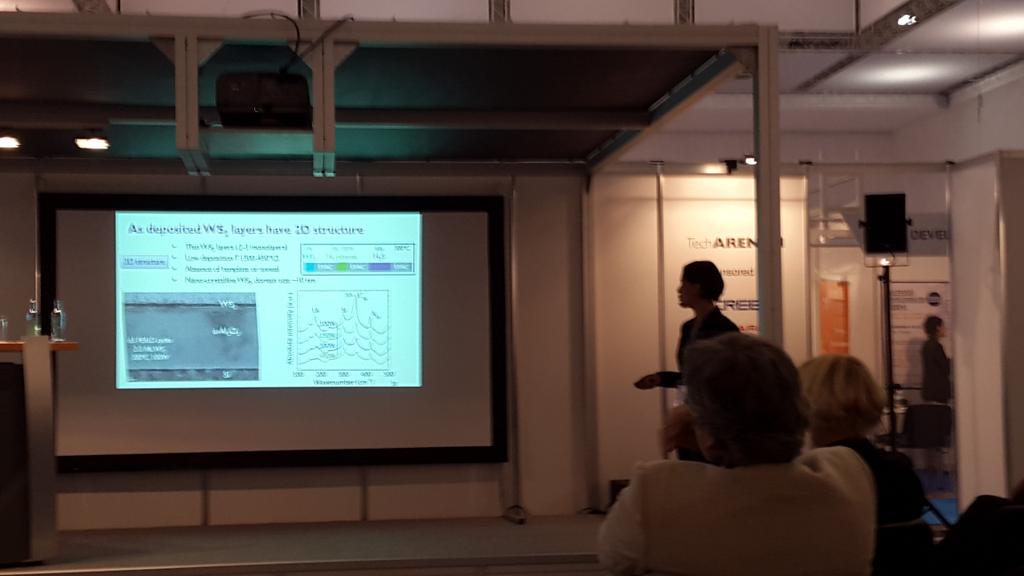
Monolayer controlled deposition of 2D transition metal dichalcogenides on large area substrates, Presented by Annelies Delabie, Imec at SEMICON Europa 6th of October 2015, in Dresden.
I also visited SEMICON Europa 2014 where imec hosted a session on 2D Materials : http://www.semiconeuropa.org/node/2786 which was very interesting. However, there are probably some years of development ahead as ITRS has 5 nm introduction in the year 2020 or 2021 ready for mass production and that node will as we know it today not employ 2D materials.
No comments:
Post a Comment