Thursday, October 15, 2015

RASIRC Methods for Safe and Stable Delivery of Hydrogen Peroxide Gas and Hydrazine Gas for ALD

Company presents technical sessions and exhibits at AVS Symposium


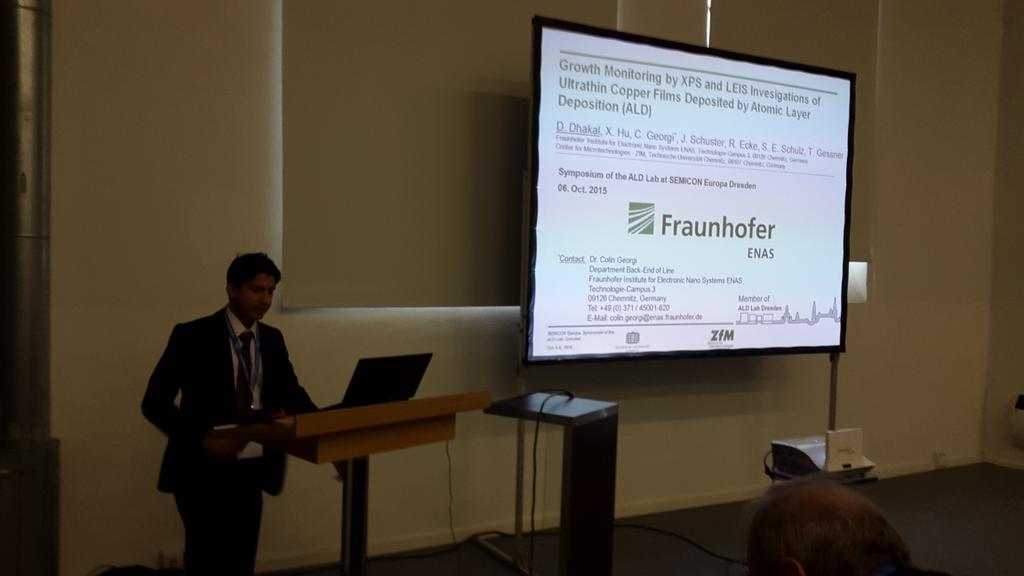
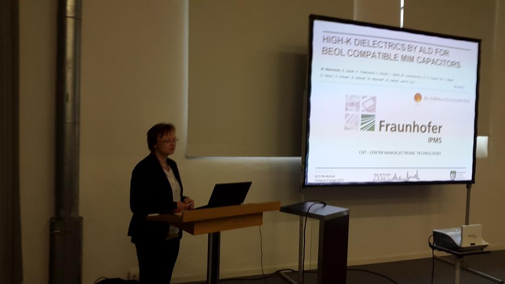
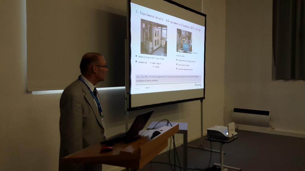
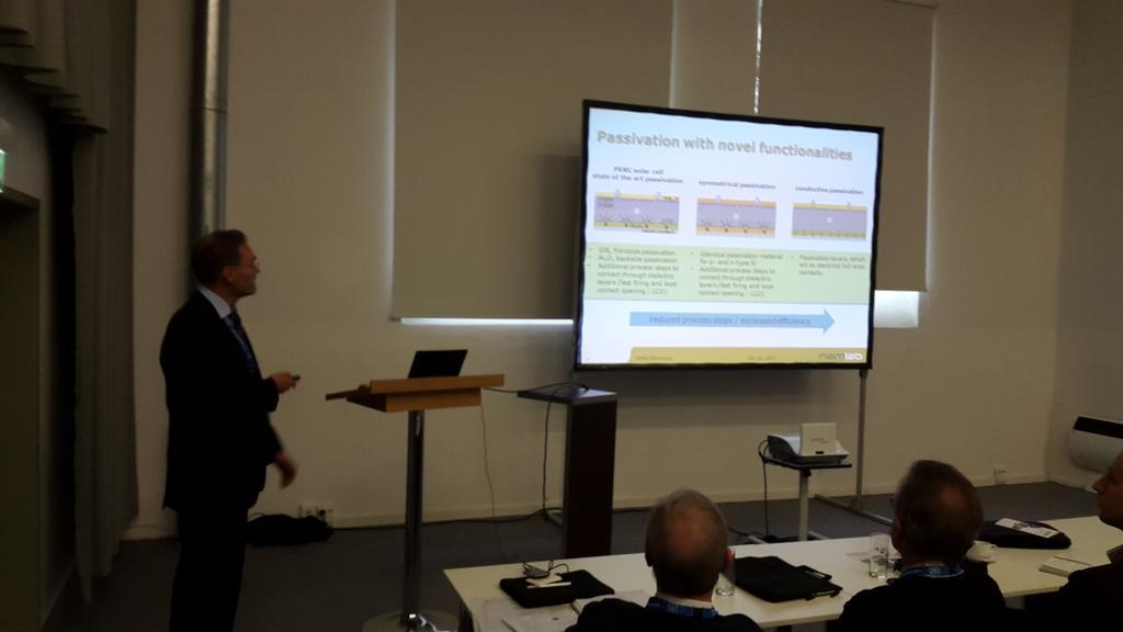
San Diego, Calif – October 14, 2015 – RASIRC will showcase a family of new technologies at the AVS 62nd International Symposium & Exhibition, October 18-23 in San Jose, California. Hydrogen peroxide gas with and without water as well as recent data on hydrazine gas for processing next generation semiconductor materials will be covered in two oral presentations and an exhibit (booth #437). The company will present “Novel Delivery of Unstable Precursors for Atomic Layer Deposition” on Monday October 19 at 4:40PM in the More Moore! II session. The company will also present “H2O2 Gas: Revolutionary new molecule for ALD” in a Technology Spotlight session.


“Next generation semiconductor devices have low thermal process budgets. Hydrogen peroxide gas and hydrazine are active molecules that allow for low temperature processing without the damage plasma can create,” said Jeffrey Spiegelman, RASIRC President and Founder. “Our Peroxidizer® and BRUTE™ product lines represent a breakthrough in stable delivery of what has been historically difficult chemicals to deliver in process.”

Hydrogen Peroxide and Hydrazine Delivery


Hydrogen peroxide in aqueous form is commonly used in semiconductor manufacturing for cleaning and surface preparation operations. However, it has limited general utility in aqueous form due to the volatility of water. In its pure state, hydrogen peroxide is highly unstable and has a propensity to decompose, forming water and oxygen. RASIRC technology uses a proprietary delivery system where 99.6% hydrogen peroxide is dissolved in non-volatile solvent.

Next generation devices have low thermal budgets and high aspect ratio structures that create new challenges for ALD grown nitride films. Hydrazine (H2NNH2) has been proposed as a thermal ALD low temperature nitride source. Hydrazine is highly flammable and its flash point decreases with reduced water content. RASIRC developed a new method and formulation for the delivery of anhydrous Hydrazine. Precursor vapor pressure is maintained at levels viable for ALD. Moreover, the addition of a proprietary solvent lowers the risk of explosion by raising the solution flash point.

Preliminary ALD data will be presented showing unique properties of these new precursors along with theoretical data on precursor delivery under variable ALD conditions.
About the Peroxidizer

The Peroxidizer is a high concentration hydrogen peroxide (H2O2) vaporizer designed specifically for the needs of next generation semiconductor processes. The Peroxidizer is the first commercial vaporizer capable of delivering concentrations greater than 5% H2O2 gas by volume from 30% H2O2 liquid source.

About BRUTE vaporizers


BRUTE Peroxide delivers anhydrous hydrogen peroxide (H2O2) for semiconductor fabrication processes such as atomic layer deposition (ALD) and atomic layer etch (ALE). BRUTE Peroxide is the only commercially available technology that can deliver up to 99.9% H2O2 gas by volume into a vacuum.

RASIRC BRUTE Hydrazine delivers water-free hydrazine (N2H4) gas into atomic layer deposition (ALD) processes. BRUTE hydrazine includes a vaporizer pre-loaded with hydrazine liquid.
AVS Symposium & Exhibition Presence

For more information about H2O2 Gas and Hydrazine delivery systems, AVS Symposium attendees are invited to visit RASIRC in booth #437. Representatives will be available to discuss technologies and test results.

Monday, October 12, 2015

New R2R ALD tool has passed factory acceptance tests at VDL ETG

According to a report on LinkedIn Flexible Electronics Group: A new R2R ALD machine operating fully at atmospheric pressure has past all factory acceptance tests this week at VDL Enabling Technologies Group (VDL ETG), The Netherlands. 


The tool can deposit various atomic layers like aluminum oxide, zinc oxide, hydrogen sulfide, etc. without making use of a vacuum chamber. The adopted technology allows for extremely fast deposition rates that can even exceed by 50-100 times the deposition rates achieved in conventional vacuum-based R2R ALD tools. Built-in air bearings guarantee the scratch-free handling of the webs used as flexible substrates. The deposition can take place at temperatures as low as 80-100 degrees Celsius, which makes this R2R ALD tool extremely useful for the deposition of barriers, buffer layers, optical films, etc. in flexible electronic devices produced on plastic foils.

ALD Dielectric film with a refractive index close to air

From North Carolina State University, here is an amazing use of ALD Al2O3 and ZnO dielectric film that has optical and electrical properties similar to air, but is strong enough to be incorporated into electronic and photonic devices - making them both more efficient and more mechanically stable. Full report here and in the actual publication below as well in this supporting information file with free access : http://onlinelibrary.wiley.com/store/10.1002/adfm.201502854/asset/supinfo/adfm201502854-sup-0001-S1.pdf?v=1&s=22a54d6412037acca3bb9709f8286a3fb4877e9f

Ordered 3D Thin-Shell Nanolattice Materials with Near-Unity Refractive Indices


Xu A. Zhang, Abhijeet Bagal, Erinn C. Dandley, Junjie Zhao, Christopher J. Oldham, Bae-Ian Wu, Gregory N. Parsons and Chih-Hao Chang
Advanced Functional Materials, DOI: 10.1002/adfm.201502854


By manipulating the structure of aluminum oxide, a dielectric material, researchers were able to improve its optical and mechanical properties. The key to the film's performance is the highly-ordered spacing of the pores, which gives it a more mechanically robust structure without impairing the refractive index. You can see the structure here, on the micrometer scale.

The refractive indices of naturally occurring materials are limited, and there exists an index gap between indices of air and available solid materials. With many photonics and electronics applications, there has been considerable effort in creating artificial materials with optical and dielectric properties similar to air while simultaneously being mechanically stable to bear load. Here, a class of ordered nanolattice materials consisting of periodic thin-shell structures with near-unity refractive index and high stiffness is demonstrated. Using a combination of 3D nanolithography and atomic layer deposition, these ordered nanostructured materials have reduced optical scattering and improved mechanical stability compared to existing randomly porous materials. Using ZnO and Al2O3 as the building materials, refractive indices from 1.3 down to 1.025 are achieved. The experimental data can be accurately described by Maxwell Garnett effective media theory, which can provide a guide for index design. The demonstrated low-index, low-scattering, and high-stiffness materials can serve as high-quality optical films in multilayer photonic structures, waveguides, resonators, and ultra-low-k dielectrics.

Sunday, October 11, 2015

Wafer-scale single-domain-like graphene by defect-selective ALD of hexagonal ZnO

Korean researchers report defect-selective atomic layer deposition (ALD) for stitching grain boundaries of CVD graphene with ZnO to increase the connectivity between grains. In the present ALD process, ZnO with a hexagonal wurtzite structure was selectively grown mainly on the defect-rich grain boundaries to produce ZnO-stitched CVD graphene with well-connected grains.

Wafer-scale single-domain-like graphene by defect-selective atomic layer deposition of hexagonal ZnO

Kyung Sun Park, Sejoon Kim, Hongbum Kim, Deokhyeon Kwon, Yong-Eun Koo Lee, Sung-Wook Min, Seongil Im, Hyoung Joon Choi, Seulky Lim, Hyunjung Shin, Sang Man Koo and Myung Mo Sung

Nanoscale, 2015, Advance Article, DOI: 10.1039/C5NR05392GAccepted 24 Sep 2015


Large-area graphene films produced by means of chemical vapor deposition (CVD) are polycrystalline and thus contain numerous grain boundaries that can greatly degrade their performance and produce inhomogeneous properties. A better grain boundary engineering in CVD graphene is essential to realize the full potential of graphene in large-scale applications. Here, we report a defect-selective atomic layer deposition (ALD) for stitching grain boundaries of CVD graphene with ZnO so as to increase the connectivity between grains. In the present ALD process, ZnO with a hexagonal wurtzite structure was selectively grown mainly on the defect-rich grain boundaries to produce ZnO-stitched CVD graphene with well-connected grains. For the CVD graphene film after ZnO stitching, the inter-grain mobility is notably improved with only a little change in the free carrier density. We also demonstrate how ZnO-stitched CVD graphene can be successfully integrated into wafer-scale arrays of top-gated field-effect transistors on 4-inch Si and polymer substrates, revealing remarkable device-to-device uniformity.

UK collaboration seeks to develop new ultra-barrier materials based on graphene interlayers & roll to roll ALD

As reported by New Electronics : The Centre of Process Innovation (CPI) has announced that it has joined a UK based collaboration called ‘Gravia’, to develop the next generation of ultra-barrier materials using graphene for the production of flexible transparent plastic electronic based displays for the next generation of smartphones, tablets and wearable electronics.


The graphene market is predicted to be worth more than £800million by 2023 and could transform the manufacturing landscape in the UK.The project, including the University of Cambridge, FlexEnable and the National Physical Laboratory (NPL), expects to deliver a feasible material and process system. It builds upon existing investments by Innovate UK and the EPSRC in this area.


CPI Cleanroom

“The collaboration brings together world class supply chain expertise across the UK to bridge the gap from Graphene research to the manufacturing of commercial flexible display screens,” said James Johnstone, business development manager at CPI. 

“CPI’s role in the project is to use roll-to-roll atomic layer deposition technologies to scale up, test and fabricate the ultra barrier materials.”


Beneq Roll to Roll Atomic Layer Deposition Tool - CPI offers a roll to roll atomic layer deposition (ALD) tool which is capable of handling films up to 600mm wide with thicknesses ranging from 20 – 200 µm and can produce an active coat width of 480mm.

The incorporation of graphene interlayers offers potential for flexible displays. Its gas blocking properties will enable barrier materials that are flexible, transparent, robust, and impervious to many molecules. Gravia will seek to accelerate product development, improving upon current ultra barrier performance and lifetimes by producing consistent barrier materials and processes on large area substrates by utilising specialist growth techniques. The key challenge will be to develop large-area poly-crystalline graphene films which maximise performance whilst mitigating process imperfections.

TEL signs $262 million deal with SUNY Poly to stay in Albany

As reported by Times Union : Tokyo Electron Ltd. has signed a five-year, $262.5 million extension of its research and development agreement with SUNY Polytechnic Institute in a deal that keeps the Japanese computer chip manufacturing equipment maker in Albany through 2020.


The agreement, which took effect Oct. 1 and will be officially announced Thursday, comes 12 years after the company, known in the industry as TEL, chose Albany for its first research lab outside of Japan.


The newly inked deal also is critical because TEL, which makes manufacturing equipment used in chip factories, or "fabs," is expected to play a key role in one or more manufacturing development programs in Albany involving at least $1 billion in spending by the semiconductor industry and hundreds of new jobs, the exact details of which have yet to be made public.


"New York continues to be a wonderful partner to TEL," Tetsuro Higashi, CEO of TEL said in a statement provided to the Times Union. "Through SUNY Poly, Gov. Cuomo has created one of the finest R&D centers in the world for creating next-generation chip technology, and we look forward to our continued collaboration and innovation."

Wednesday, October 7, 2015

3M licensing agreement with Lotus Applied Technology TransFlexALDTM spatial ALD

As reported today : 3M has entered into a licensing agreement with Lotus Applied Technology to access Lotus’s TransFlexALDTM spatial Atomic Layer Deposition (ALD) and barrier materials patent portfolio. TransFlexALD technology enables high-speed, low-cost deposition of single layer “ultra-barrier” coatings on rolls of polymer film using ALD. These coatings play a critical role in the encapsulation of moisture- and oxygen-sensitive electronics, such as OLED (organic light emitting device) lighting and displays, quantum dot films, photovoltaics, and flexible electronics.


“We are pleased to partner with Lotus AT and for the potential of their ALD technology to expand our ultra barrier film solutions portfolio as we integrate it with 3M’s proven technology strengths,” said John Banovetz, vice president of 3M’s Corporate Research Laboratory. “This licensing agreement and our continued product innovation will help 3M increase the performance of our ultra barrier films and offer cost-effective barrier solutions that will allow our customers to provide more competitive products in the flexible electronics markets they serve.”

3M is a leading manufacturer of flexible, transparent ultra barrier films providing encapsulation solutions for display (3M™ Flexible Transparent Barrier Film) and other sensitive electronic applications.


“We are excited to partner with 3M, a distinguished technology leader in the field of ultra barrier films,” said Eric Dickey, president of Lotus Applied Technology. “This technology offers the opportunity to radically improve the performance of single-layer barrier coatings, and 3M’s experience and expertise in this field will enable its rapid deployment in a field of applications that have been demanding higher performance at lower cost.”


(http://lotusat.com) Founded in 2007, Lotus Applied Technology was formed through a spinoff of the thin film process group within Planar Systems, Inc., a pioneer in Atomic Layer Deposition technology and manufacturing. Housed in a fully dedicated 20,000 square foot thin film processing and R&D facility in Hillsboro, Oregon, our team of technologists has been working together for over 20 years, developing innovative solutions to thin film processing challenges. Our equipment set includes a wide array of thin film deposition, lithography, and patterning equipment, including a versatile set of ALD equipment:

  • Six P400 Conventional Pulse-Based Batch ALD reactors
  • Roll to Roll ALD Research Scale Reactor
  • TransFlex Roll to Roll ALD Pilot Scale Reactor
  • Vortex Rotary Batch Reactor

Atomic Layer Processing at SEMICON Europa 2015

Here are some ALD related pictures from SEMICON Europa in Dresden. Not only ALD since this year ALE and RIE was also a hot topic in the afternoon of the ALD Lab Dresden Symposium on Tuesday (see previous post). Biggest news here is that Oxford Instruments has released new innovative hardware for ALE!


Oxford Instruments releasing new innovative hardware for ALE (Atomic Layer Etching). Harm Knoops (right) and Andreas Stamm (left)


Assuming Oxford Instrument have big success with selling ALE hardware we will definitely start seeing an increase in ALE publications in the future and maybe the upward trend of ALD will follow or the technologies will merge into one for "Atomic Layer Processing" or like some of  us like to call it - ALX. This was actually the message from many of the presenter in the ALD Symposium (Prof. Bartha, Prof. Roozeboom, and Stephan Wege from Plasway), including this one from myself. The OEM market for ALX will definitely be very innovative and interesting in the years to come.


The Sentech stand a German OEM selling both Etch, PECVD and ALD / PEALD equipment together with very powerful in-situ ellipsometry metrology.


Nice to see that there is a lot of new activities in the European precursor supplier business. Here the team from EpiValence. EpiValence is focusing on working in collaboration with organisations looking for advanced chemicals and materials. Starting with research and development through to full scale up. You may also notice the close collaboration with iCAM (see their stand futher below)


A cross section of the popular Japanese ALD valves from KTZ SCT


Plasma Therm makes very technological advanced ICP RIE tools (Versaline) with lamp heated (!) chambers. Why these guys don´t make a PEALD chamber I don´t know - fast gas switching they do master for their Plasma wafer dicing process, which seems to be their cash cow.


Quick stop at the STREM  to talk to Jamal Belgacem about some need for new precursor and to pick up the latest catalogues for ALD precursors


I had a nice chat with Peter Barlow at iCAM - The Bubbler Maters from Wales - about building a new flexible solid evaporator for precursor screening. 


Tuesday, October 6, 2015

Photoshow : ALD Lab Dresden Symposium at SEMICON Europa 2015

SEMICON Europa this year has turned out to be a major event for ALD and exciting nanoelectronic materials research. Here are photos taken from The ALD Day October 6th, 2015!

More details on this event you can find here : http://baldengineering.blogspot.de/2015/10/ald-ale-and-exciting-nanoelectronic.html

We are already looking forward to SEMICON Europa 2016 in Grenoble, France and to co-chair an ALD Sympoium there yet one more time!

SEMICON Europa ALD 2014, Grenoble : http://baldengineering.blogspot.de/2014/10/voila-3rd-ald-lab-dresden-symposium-at.html


Columbus, Tuesday Oct 6, 13:45, ALD / ALE Sympoium of The ALD Lab Dresden, Messe Dreaden, Germany


Waiting for the ALD Storm!


Welcome
Prof. Johann W. Bartha, TU Dresden


In situ monitoring of Atomic Layer Deposition in porous materials
Martin Knaut, TU Dresden


Passivation of MEMS by Atomic Layer Deposition
Matthias Schwille, Robert Bosch


Symposium is full - please help me throw out a PVD guy


Growth Monitoring by XPS and LEIS Investigations of Ultrathin Copper Films Deposited by Atomic Layer Deposition
Dileep Dhakal, TU Chemnitz/FhG ENAS


High-k dielectrics by ALD for BEOL compatible MIM
Wenke Weinreich, FhG IPMS-CNT


ALD coatings for applications as permeation barrier and protective layer in fiber-reinforced materials
Mario Krug, FhG IKTS


ALD for solar cell application
Ingo Dirnstorfer, NaMLab


Plasma enhanced ALD process for TiO2- and WO3- films
Alexander Strobel, FH Zwickau


Why do we need Atomic Layer Etching
Jonas Sundqvist, Lund University/TU Dresden


Spatial Atomic Layer Deposition and Atomic Layer Etching
Prof. Fred Roozeboom, TU Eindhoven / TNO Eindhoven


Atomic Layer Etching: What Can We Learn from Atomic Layer Deposition?
Harm Knoops, Oxford Instruments/TU Eindhoven


Hardmask and side wall protection during dry etching with plasma enhanced deposition during dry etching for ALE purposes
Stephan Wege, Plasway


Industrial High Throughput Atomic Layer Deposition Equipment and Process for OLED Encapsulation
Jacques Kools, Encapsulix


Monolayer controlled deposition of 2D transition metal dichalcogenides on large area substrates
Annelies Delabie, Imec


Selective Deposition as Enabler for Shrinking Device Dimensions

Suvi Haukka, Executive Scientist, ASM Microchemistry Ltd.


Saturday, October 3, 2015

TECHCET -Dielectric Precursors – NEW – Just Released!

The Dielectric Precursors Report provide detailed market, supply chain and technology trend information required for anyone developing strategy for their business, be it a materials supplier or semiconductor chip manufacturer. Precursor types include, gapfill, ILD, low K, and multi-patterning.


Click here for full table of contents:


Workshop Simulation of chemistry-driven growth phenomena for metastable materials

CECAM/Psi-k/HERALD Workshop
Simulation of chemistry-driven growth phenomena for metastable materials


The controlled growth of thin films based on metastable materials by chemistry-driven processes is of high technological importance for topics like semiconductor devices or optical coatings. Computational modelling of this inherently multiscale process is crucial for an atomistic understanding and enables a decoupling and separate optimization of the growth-determining factors of non-equilibrium materials. This workshop will result in a joint effort by experts from different modelling communities covering the necessary length and time scales.
The workshop will be held at

nearby Marburg in Germany from November 08-11, 2015.
 

Organizers

CECAM Psi-k HERALD
   

Sponsors

GRK 1782 ESFDock/Chemicals